Sizing up MI300A’s GPU
AMD’s Instinct MI300A is a giant APU, created by swapping out two GPU chiplets (XCDs) for three CPU chiplets (CCDs). Even though MI300A integrates Threadripper-like CPU muscle, the chip’s main attraction is still its massive GPU compute power. Here, we’re going to size up MI300A’s GPU and see where it stands using comparison data from a few other GPUs, including MI300X.
Acknowledgments
Special thanks goes out to AMD and GIGABYTE along with their Launchpad service , who generously let Chips and Cheese play around with a massive quad-socket MI300A system system in the form of the G383-R80-AAP1 for over 2 weeks. As always, our testing was our own.
We also have limited data from Nvidia’s H100. H100 comes in both a PCIe and SXM5 version. I (Clam) rented a H100 PCIe cloud instance for the MI300X article from before. Cheese/Neggles rented a H100 SXM5 instance for benchmarking against the MI300A.
OpenCL Compute Throughput
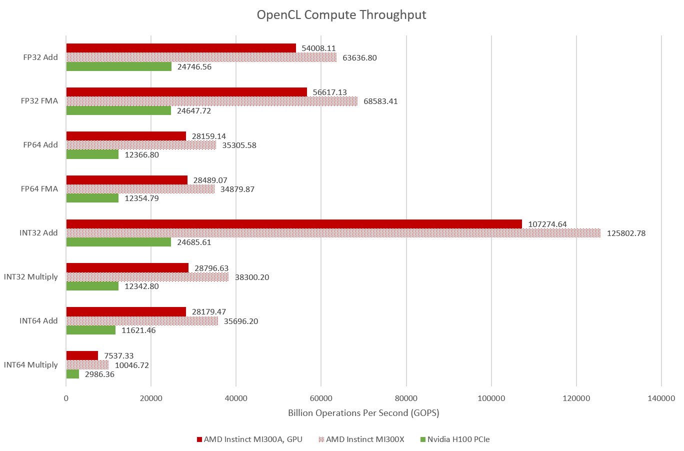
MI300A may be down a couple XCDs compared to its pure GPU cousin, but it still has plenty of compute throughput. It’s well ahead of Nvidia’s H100 PCIe for just about every major category of 32-bit or 64-bit operations. H100’s SXM5 variant should slightly increase compute throughput, thanks to its higher SM count. But a 16% increase in SM count likely won’t do much to close the gap between H100 and either MI300 variant.
MI300A can achieve 113.2 TFLOPS of FP32 throughput, with each FMA counting as two floating point operations. For comparison, H100 PCIe achieved 49.3 TFLOPS in the same test.
Even though GPUs are vector throughput monsters, modern CPUs can pack pretty respectable vector throughput too. I’ve written a CPU-side multithreaded vector throughput test, mostly for fun. Using AVX-512, MI300A’s 24 Zen 4 cores can sustain 2.8 TFLOPS. That’s quite a bit compared to some older consumer GPUs. But MI300A’s GPU side is so massive that CPU-side throughput is a rounding error.
MI300A therefore strikes a very different balance between CPU and GPU size compared to a typical consumer integrated graphics solution like AMD’s Hawk Point. The Ryzen 7 PRO 8840HS’s Radeon 780M iGPU is no slouch with basic 32-bit operations, but CPU-side vector throughput is still significant.
Consumer GPU architectures de-emphasize FP64 throughput, so the 8840HS’s eight Zen 4 cores can provide more throughput than than the GPU side. Zen 4 also holds an advantage with integer multiplication, though it’s not as big as with FP64. From a compute throughput perspective, MI300A is more like a GPU that happens to have a CPU integrated.
First Level Cache Bandwidth
Measuring cache bandwidth is another way to size up the MI300A. Here, I’m testing load throughput over a small 1 KB array. That should fit within L1 on any GPU. Normally, I use an image1d_buffer_t buffer because some older Nvidia GPUs only have a L1 texture cache, and plain global memory loads go through to L2. But AMD’s CDNA3 architecture doesn’t support texture operations. It’s meant to handle parallel compute after all, not rasterize graphics. Therefore, I’m using global memory accesses on both the MI300X and MI300A.
L1 bandwidth paints a similar picture to compute throughput. MI300A’s GPU is a slightly smaller MI300X, a bit like how AMD’s HD 7950 is a slightly smaller HD 7970. Again, the massive scale of AMD’s MI300 platform lets it leave Nvidia’s H100 in the dust even after making room for 24 CPU cores. The consumer oriented RX 6900XT also turns in a good showing, because it has very high L1 bandwidth L1 vector caches and runs at higher clock speeds.
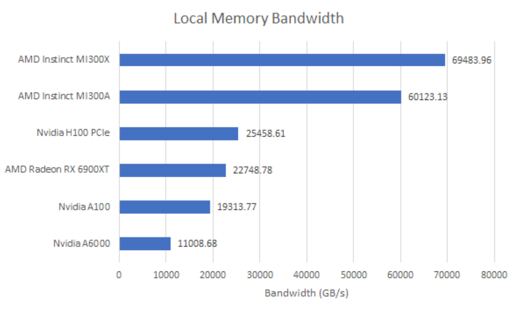
Besides caches, GPUs offer a local memory space only visible within a workgroup of threads. AMD GPUs back this up with a Local Data Share within each Compute Unit, while recent Nvidia GPUs allocate local memory out of their L1 caches.
MI300 GPUs have tons of local memory bandwidth on tap, with both variants pushing past 60 TB/s. Everything else gets left in the dust.
Atomics Throughput
Atomic operations can be useful for multithreaded applications, because they let a thread guarantee that series of low-level operations happens without interference from any other thread. For example, adding a value to a memory location involves reading the old value from memory, performing the add, and writing the result back. If any other thread accesses the value between those operations, it’ll get stale data, or worse, overwrite the result.
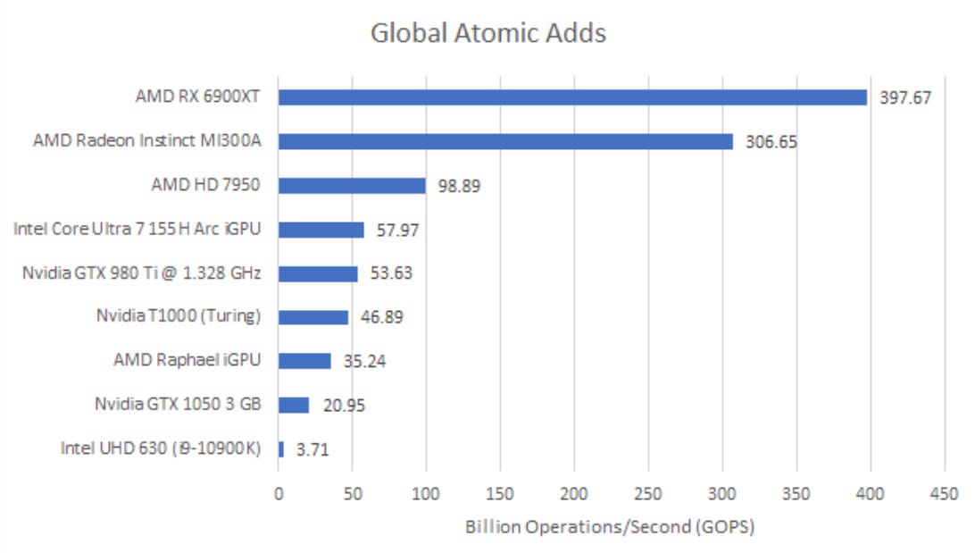
GPUs handle global memory atomics using special execution units at the L2 slices. In contrast, CPU cores handle atomics by retaining ownership of a cacheline until the operation completes. That means GPU atomic throughput can be constrained by execution units at the L2, even without contention. MI300A has decent throughput for atomic adds to global memory, though it falls short of what I expect. AMD’s GPUs had 16 atomic ALUs per L2 slice since GCN. I get close to that on my RX 6900 XT, but not on MI300A.
Because atomic adds are a read-modify-write operation, 306.65 billion operations per second on INT32 values translates to 2.45 TB/s of L2 bandwidth. On the 6900XT, 397.67 GOPS would be 3.2 TB/s. Perhaps MI300A has to do something special to ensure atomics work properly across such a massive GPU. Compared to a consumer GPU like the 6900XT, MI300A’s L2 slices don’t have sole ownership of a chunk of the address space. One address could be cached within the L2 on different XCDs. A L2 slice carrying out an atomic operation would have to ensure no other L2 has the address cached.
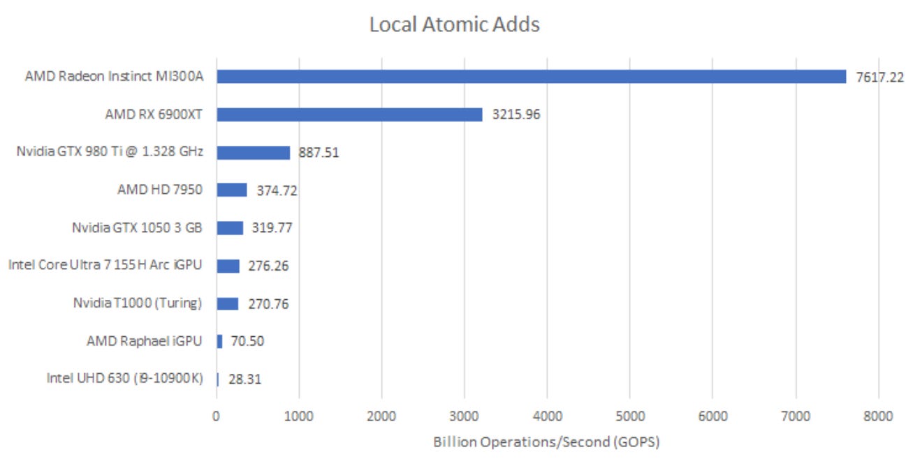
OpenCL also allows atomic operations on local memory, though of course local memory atomics are only visible within a workgroup and have limited scope. But that also means the Compute Unit doesn’t have to worry about ensuring consistency across the GPU, so the atomic operation can be carried out within the Local Data Share. That makes scaling throughput much easier.
Now, atomic throughput is limited by the ALUs within MI300’s LDS instances. That means it’s extremely high, and leaves the RX 6900XT in the dust.
FluidX3D
FluidX3D uses the lattice Boltzmann method (LBM) to simulate fluid behavior. It features special optimizations that let it use FP32 instead of FP64 while still delivering good accuracy in “all but extreme edge cases.” In FluidX3D’s built-in benchmark, MI300A’s GPU lands closer to its larger cousin than microbenchmarks and specification sheets would suggest. The MI300A server we tested uses air cooling, so its default power target is 550W per GPU. MI300A is just 1% slower than MI300X at that power setting. With a higher 760W power target, MI300A manages to lead its nominally larger GPU-only sibling by 4.5%.
Testing FluidX3D is complicated because the software is constantly updated. Part of MI300A’s lead could be down to optimizations done after we tested MI300X back in June. FluidX3D also tends to be very memory bound when using FP32, so similar results aren’t a surprise. Both MI300 variants continue to place comfortably ahead of Nvidia’s H100, though the SXM5 variant does narrow the gap somewhat. H100’s SXM5 variant uses HBM3, giving it 3.9 TB/s of DRAM bandwidth compared to 3.35 TB/s on the H100 PCIe, which uses HBM2e.
Because FluidX3D is so heavily limited by memory bandwidth, the program can use 16-bit formats for data storage. Its FP16S mode uses IEEE-754’s FP16 format for storage. To maximize accuracy, it converts FP16 values to FP32 before doing computation. GPUs often have hardware support for FP16-to-FP32 conversion, which minimizes computation overhead from using FP16S for storage.
MI300A and H100 both see improved performance in FP16S mode, and MI300A continues to hold a large advantage.
FluidX3D also has a FP16C mode, which uses a custom FP16 format. The mantissa field gets an extra bit, which is taken away from the exponent field. That improves accuracy while using the same memory bandwidth as FP16S mode. However, GPUs won’t have hardware support for converting a custom FP16 format to FP32. Conversion therefore requires a lot more instructions, increasing compute demands compared to FP16S mode.
MI300A continues to stay ahead of H100 in FP16C mode. AMD has built a much larger GPU from both the compute and memory bandwidth perspective, so MI300A has an advantage regardless of whether FluidX3D wants more compute or memory bandwidth.
Power target also matters more in FP16C mode. Going from 550W to 760W improves performance by 12.4% in FP16C mode. In FP32 or FP16S mode, going up to 760W only gave 5.3% or 6.5% more performance, respectively. Likely, FP16C mode’s demand for more compute along with its still considerable appetite for memory bandwidth translates to higher power demand.
Calculate Gravitational Potential (FP64)
Large compute GPUs like MI300 and H100 differentiate themselves from consumer GPUs by offering substantial FP64 throughput. Client GPUs have de-prioritized FP64 because graphics rendering doesn’t need that level of accuracy.
This is a self-penned workload by Clam (Chester), based on a long running workload from a high school internship. The program takes a FITS image from the Herschel Space Telescope with column density values, and carries out a brute force gravitational potential calculation. The original program written back in 2010 took a full weekend to run on a quad core Nehalem system, and was written in Java. I remember I started it before leaving the office on a Friday, and it finished after lunch on Monday. Now, I’ve hacked together a GPU accelerated version using OpenCL.
AMD’s MI300A completes the workload in 17.5 seconds, which is a bit shorter than a weekend. I wish I had this sort of compute power back in 2010. Nvidia’s H100 PCIe manages to finish in 54 seconds. That’s still very fast, if not as fast as MI300A. Both datacenter GPUs are faster than the integrated GPU on the Ryzen 9 7950X3D, which takes more than four hours to finish the task.
Comparing the three MI300 results is interesting too. MI300A’s GPU is smaller than the MI300X, and that’s clear from FP64 synthetic tests. When measuring compute throughput, I keep all values in registers. But a workload like this exercises the cache subsystem too, and data movement costs power. I should barely hit DRAM because my input data from 2010 fits within Infinity Cache. But still, my code makes MI300A use all the power it can get its hands on. Going from a 550W to 760W power target increases performance by 12.4%, which curiously puts MI300A ahead of MI300X. I wasn’t expecting that.
On one hand, I’m impressed at how much a power target difference can make. On the other, a 38% higher power target only improves performance by 12.4%. I’m not sure if that’s a great tradeoff. That’s a lot of extra power to finish the program in 17.5 seconds instead of 19.7 seconds.
GROMACS
GROMACS simulates molecular dynamics. Here, Cheese/Neggles put MI300A and H100 SXM5 through their paces on the STMV benchmark system. Again, both MI300 variants land in different performance segments compared to Nvidia’s H100.
Again, bigger power targets translate to higher performance. In GROMACS, MI300A enjoys a 15% performance gain in 760W mode. It’s even larger than in my gravitational potential computation workload or FP16C mode on FluidX3D.
Final Words
AMD has to cut down MI300X’s GPU to create the MI300A. 24 Zen 4 cores is a lot of CPU power, and occupies one quadrant on the MI300 chip. But MI300’s main attraction is still the GPU. AMD’s integrated graphics chips in the PC space are still CPU-first solutions with a big enough iGPU to handle graphics tasks or occasional parallel compute. MI300A by comparison is a giant GPU that happens to have a CPU integrated. Those 24 Zen 4 cores are meant to feed the GPU and handle code sections that aren’t friendly to GPU architectures. It’s funny to see a 24 core CPU in that role, but that’s how big MI300A is.
On the GPU side, MI300A punches above its weight. Synthetics clearly show it’s a smaller GPU than MI300X, but MI300A can hold its own in real workloads. Part of that is because GPU workloads tend to be bandwidth hungry, and both MI300 variants have the same memory subsystem. Large GPUs are often power constrained too, and MI300A may be making up some of the difference by clocking higher.
At a higher level, AMD has built such a massive monster with the MI300 platform that it has no problem kicking H100 around, even when dropping some GPU power to integrate a CPU. It’s an impressive showing because H100 isn’t a small GPU by any means. Products like MI300A and MI300X show AMD now has the interconnect and packaging know-how to build giant integrated solutions. That makes the company a dangerous competitor.
And again, we’d like to give a massive shout out to GIGABYTE and their Launchpad service without whom this testing would not be possible without!
If you like the content then consider heading over to the Patreon or PayPal if you want to toss a few bucks to Chips and Cheese. Also consider joining the Discord.


I want a workstation with this monster (the same way I wanted a Xeon Phi one - and never got it).
Changing the power target from 550W to 760W doesn't necessary mean 38 percent higher power consumption. If the performance increased by 12.4 percent, could the percent increase in actual power consumption of the node as a whole be similar or even less?