
Qualcomm’s Snapdragon X2 Elite

Hello you fine Internet folks,
Last week I was in San Diego at Qualcomm’s Headquarters where Qualcomm disclosed more information about their upcoming Snapdragon X2 Elite SOC.
Snapdragon X2 Elite is Qualcomm’s newest SOC for the Windows on ARM ecosystem that is designed to bring a new level of performance so let’s dive in.
Oryon Gen 3 Prime CPU Cores and Cluster
The Snapdragon X2 Elite (SDX2E) comes equipped with a total of 18 CPU cores with 12 “Prime” cores and 6 “Performance” cores.
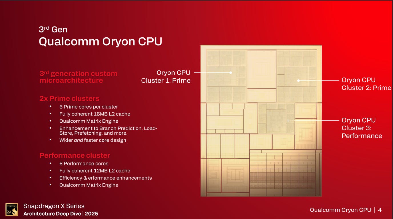
Starting with the Prime cores, these are the real heart of the SDX2E SoC with a total of up to 12 cores split across 2 clusters that can clock up to 5.0 GHz.
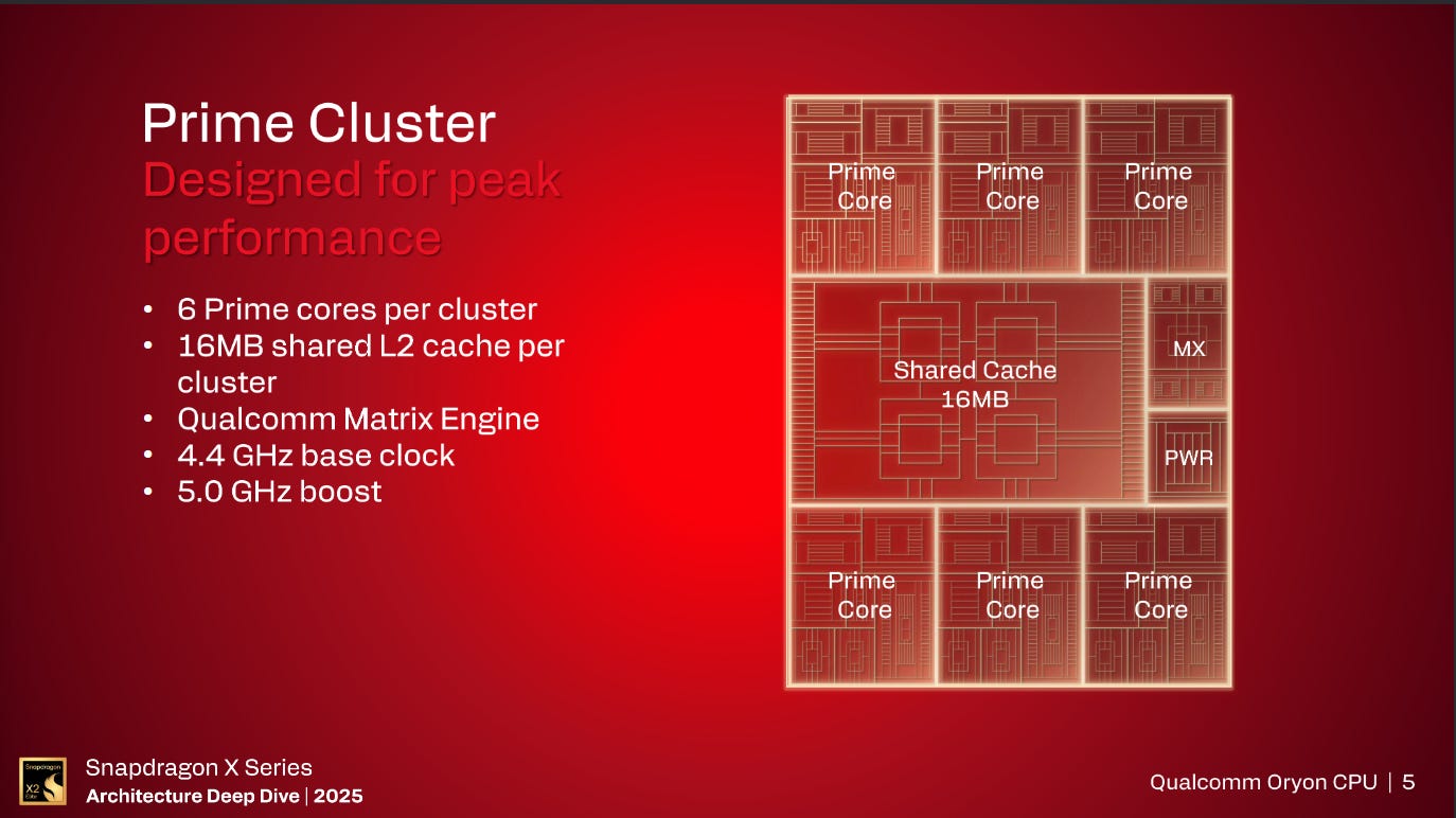
Each of these clusters has 16MB, 16-way associative, shared L2 cache with 6 Prime cores attached along with a Qualcomm Matrix Engine per cluster.
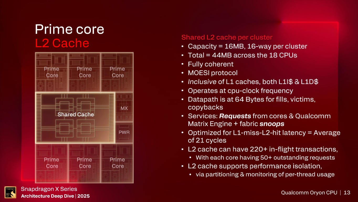
The L2 can serve up to 64B per cycle per core with a total fill bandwidth of up to 256B per cycle for the cluster. The L1 miss to L2 hit latency is now 21 cycles, up from the 17 cycles of the Snapdragon X Elite (SDXE). The reason for this increase is due to the increased size of the structure. The L2 runs at the same clocks as the cores and supports over 220 in-flight transactions with each core supporting over 50 requests to the L2 at a time.
Diving into the CPU cores and there is quite a bit familiar with this core at a high level.
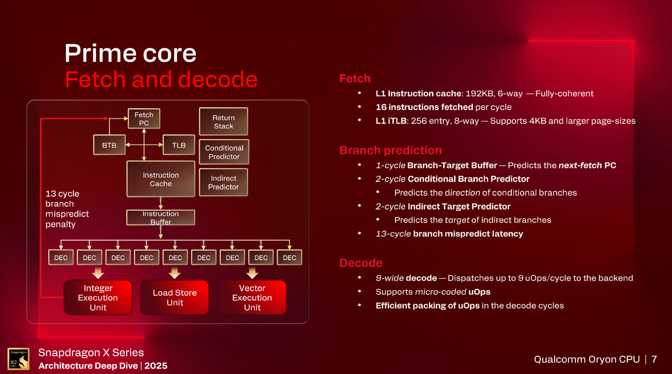
Starting with the L1 instruction cache, it is 192KB in size with 6-way associativity and is fully coherent. The Fetch Unit can fetch up to 16 4 Byte instructions per cycle for a total fetch bandwidth of 64 Bytes per cycle. The L1 iTLB is an 8-way associative, 256 entry structure that supports 4KB and larger page sizes.
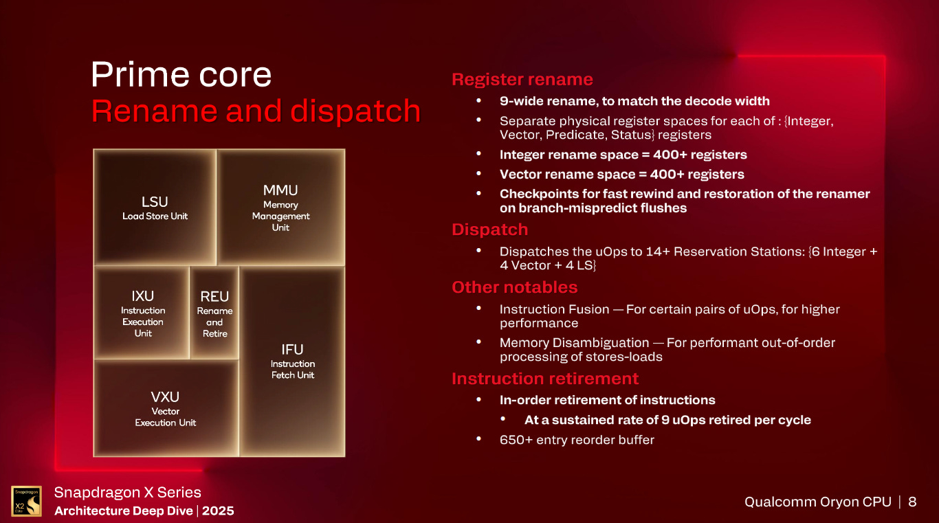
Moving to the Decode, Rename, and Retirement stages, Oryon Gen 3 has increased these stages up to 9 wide from the 8 wide that Oryon Gen 1 was meaning that Oryon Gen 3 can support up to 9 micro-ops retired per cycle. There are over 400 Vector and Integer registers in their respective physical register files which is similar to the number of entries in Oryon Gen 1. Similarly, the Reorder Buffer is similarly 650+ entries for Oryon Gen 3.
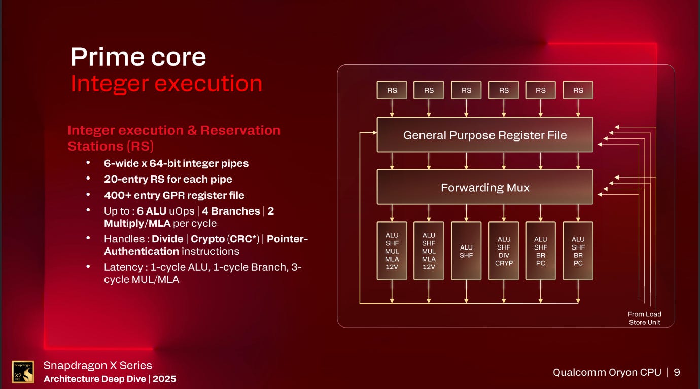
Delving into the Integer side of the core, Oryon Gen 3 now has 4 Branch units which is a doubling of the number of Branch units found inside Oryon Gen 1. Otherwise, the integer side of Oryon Gen 3 is very similar to Oryon Gen 1 with 6 20-entry Reservation Stations for a total of 120 entries in the Integer scheduler, 6 Integer ALUs with 2 capable of Multiplies and one unit capable of handling Crypto and Division instructions.
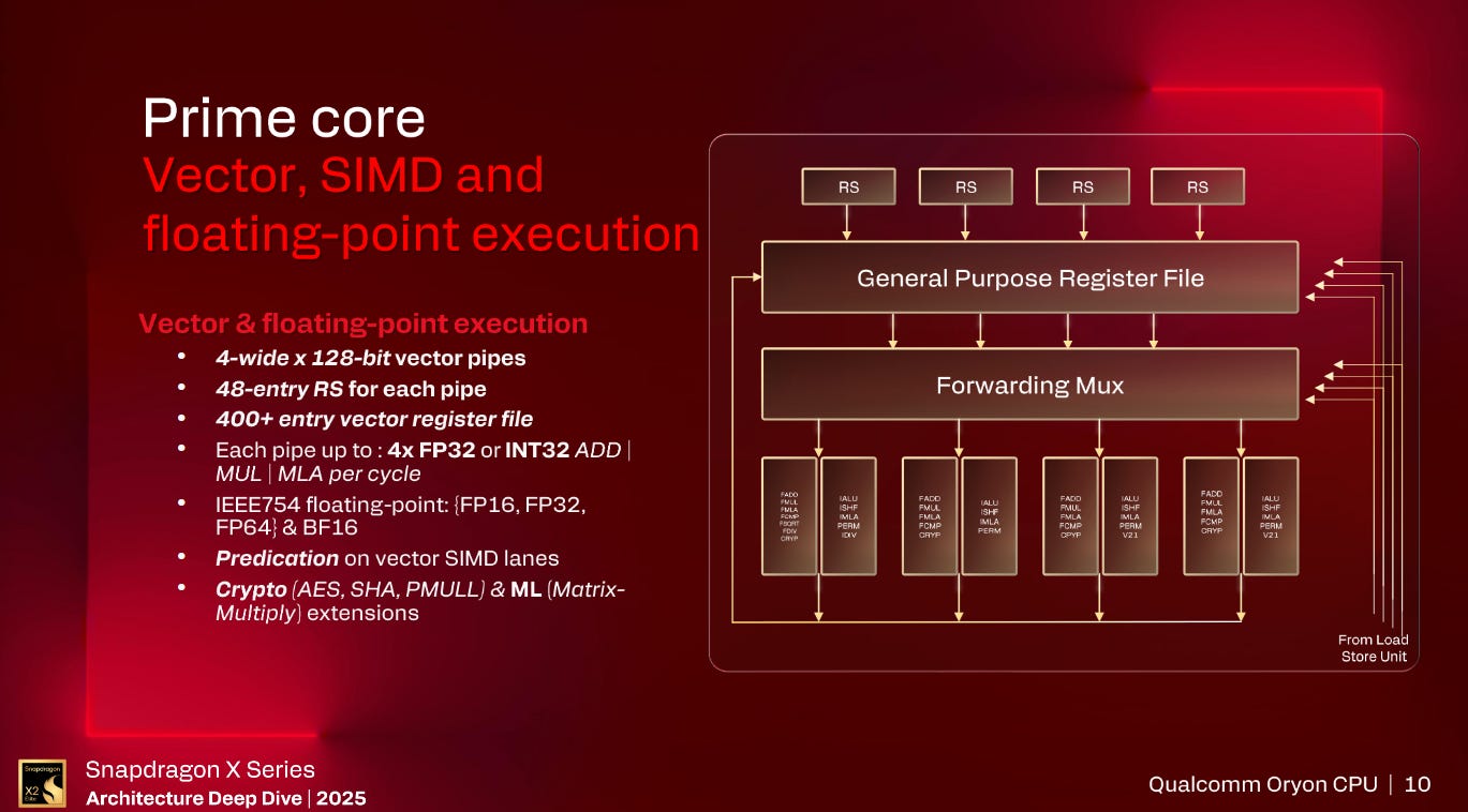
Swapping to the Vector unit and Oryon Gen 3 adds SVE and SVE2 support to the core with the high-level layout similar to Oryon Gen 1 with over 400 128b Vector registers, 4 128b Vector ALUs all capable of FMAs, and 4 48-entry Reservation Stations for a total of 192 entries in the Vector scheduler.
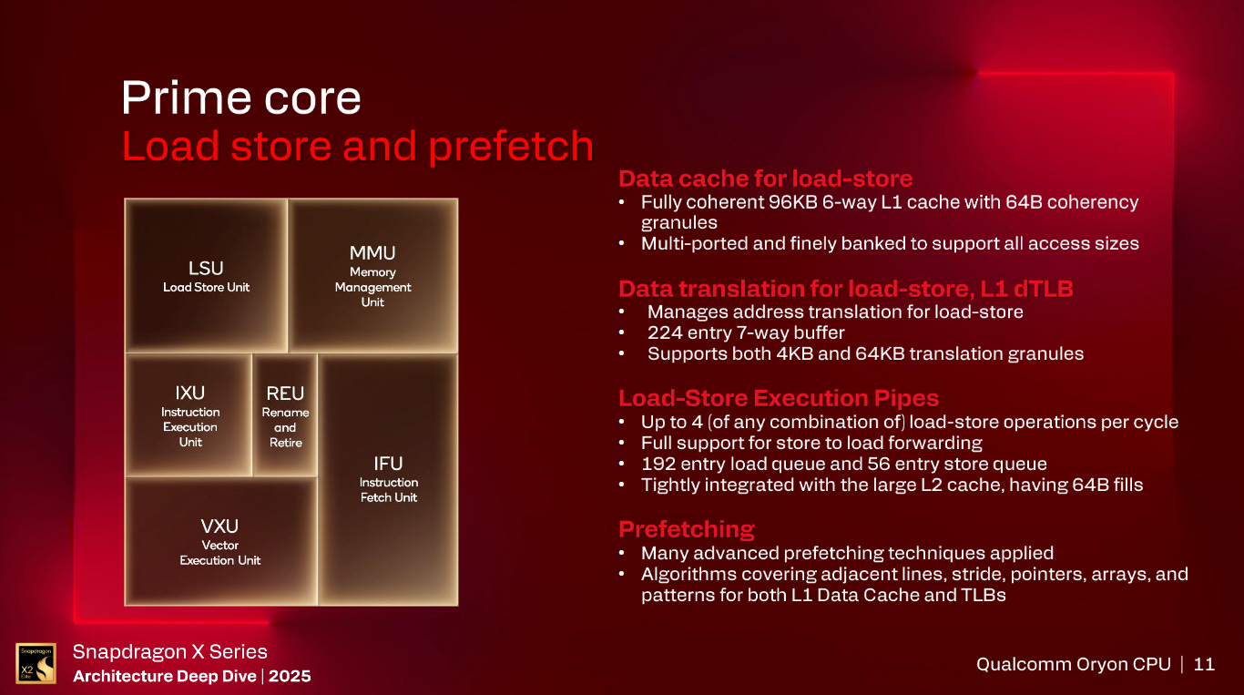
Moving to the Load and Store system, Oryon Gen 3 has the same 4 Memory AGUs all of which are capable of loads and stores as Oryon Gen 1. These then feed a 192 entry Load Queue and 56 entry Store Queue which are the same size as the queues found on Oryon Gen 1. The L1 Data Cache is also the same fully coherent 96KB, 6-way. 64 Byte cache line, structure as what Oryon Gen 1 had.
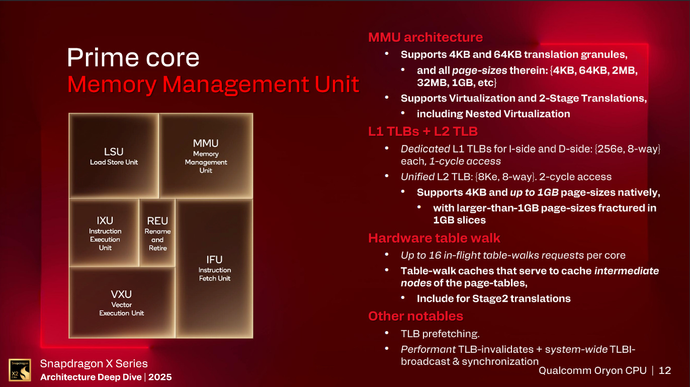
Landing at the Memory Management Unit, and the TLBs of Oryon Gen 3 are again very similar to Oryon Gen 1 with one possible difference. Slide 11 says that the L1 dTLB is a 224 entry, 7-way, structure whereas Slide 12 says that the L1 dTLB is a 256 entry, 8-way, structure. If Slide 12 is correct then this is an increase from Oryon Gen 1’s 224 entry, 7-way, L1 dTLB. Oryon Gen 3’s 256 entry, 8-way, L1 iTLB and 8K entry, 8-way, shared L2 is unchanged from Oryon Gen 1. Note, the 2 cycle access for the L2 TLB is the SRAM access time not the total latency for a TLB lookup which Qualcomm wouldn’t disclose but is a similar range to the ~7 cycles you see on modern x86 cores.
Qualcomm’s Matrix Engine
In each of SDX2E’s 3 clusters lies a SME compatible Matrix Engine.
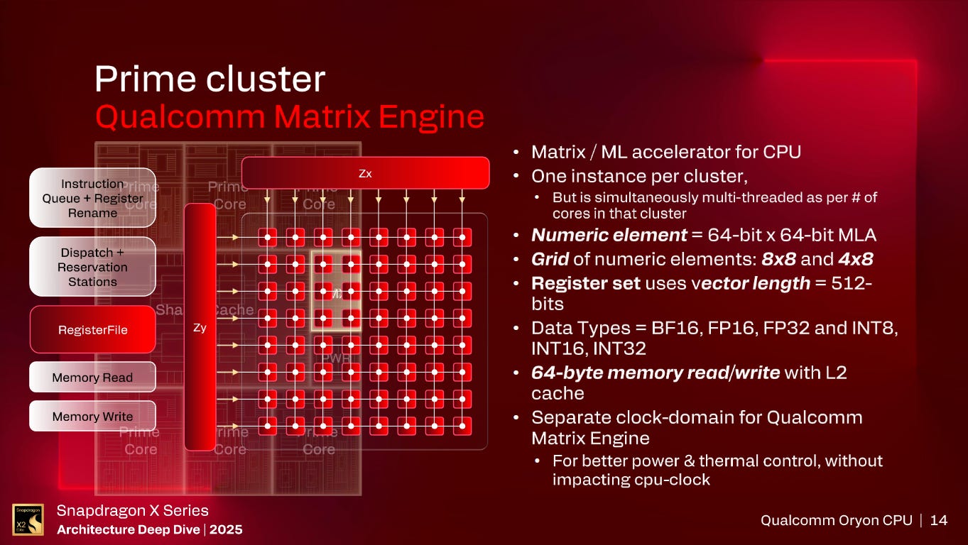
This matrix unit uses a 64 bit x 64 bit MLA numeric element in a 8x8 or 4x8 grid. This means that this matrix unit is 4096 bit wide which can do up to 128 FP32/INT32, 256 FP16/BF16/INT16, or 512 INT8 operations per cycle. The matrix engine is on a separate clock domain to the Cores and L2 Cache for better power and thermal management of the SoC.
Qualcomm Oryon Gen 3 Performance Core and Cluster
Something that is new to the SDX2E that SDXE didn’t have is a 3rd cluster on board with what Qualcomm is calling their “Performance cores”.
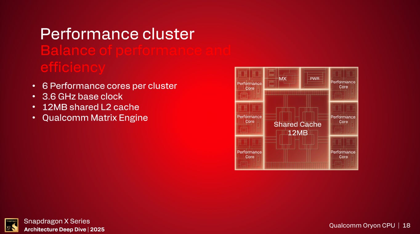
This cluster has the same number of cores along with the Matrix Engine as the Prime Clusters but instead of 16 MB of shared L2, the Performance Cluster has 12 MB of shared L2.
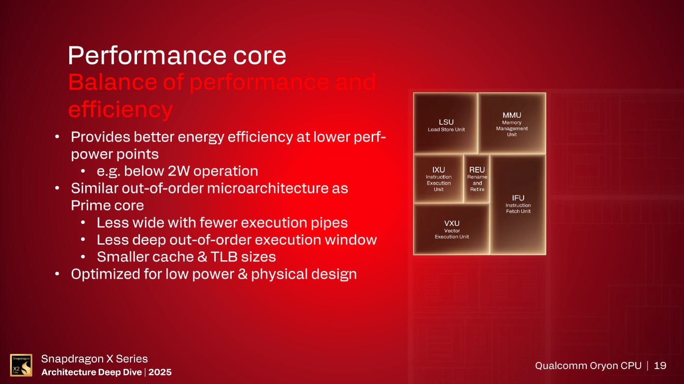
The Performance core is also different to the Prime cores. These cores are of a similar but distinct microarchitecture to the Prime cores. These cores are targeted at a lower power point and has been optimized for operation below 2 watts. As such, the Performance core isn’t as wide as the Prime core and has fewer execution pipes, smaller caches, and shallower Out-of-Order structures compared to the Prime core.
Adreno X2 GPU
SDX2E has a revamped GPU architecture that Qualcomm is calling the Adreno X2 microarchitecture.
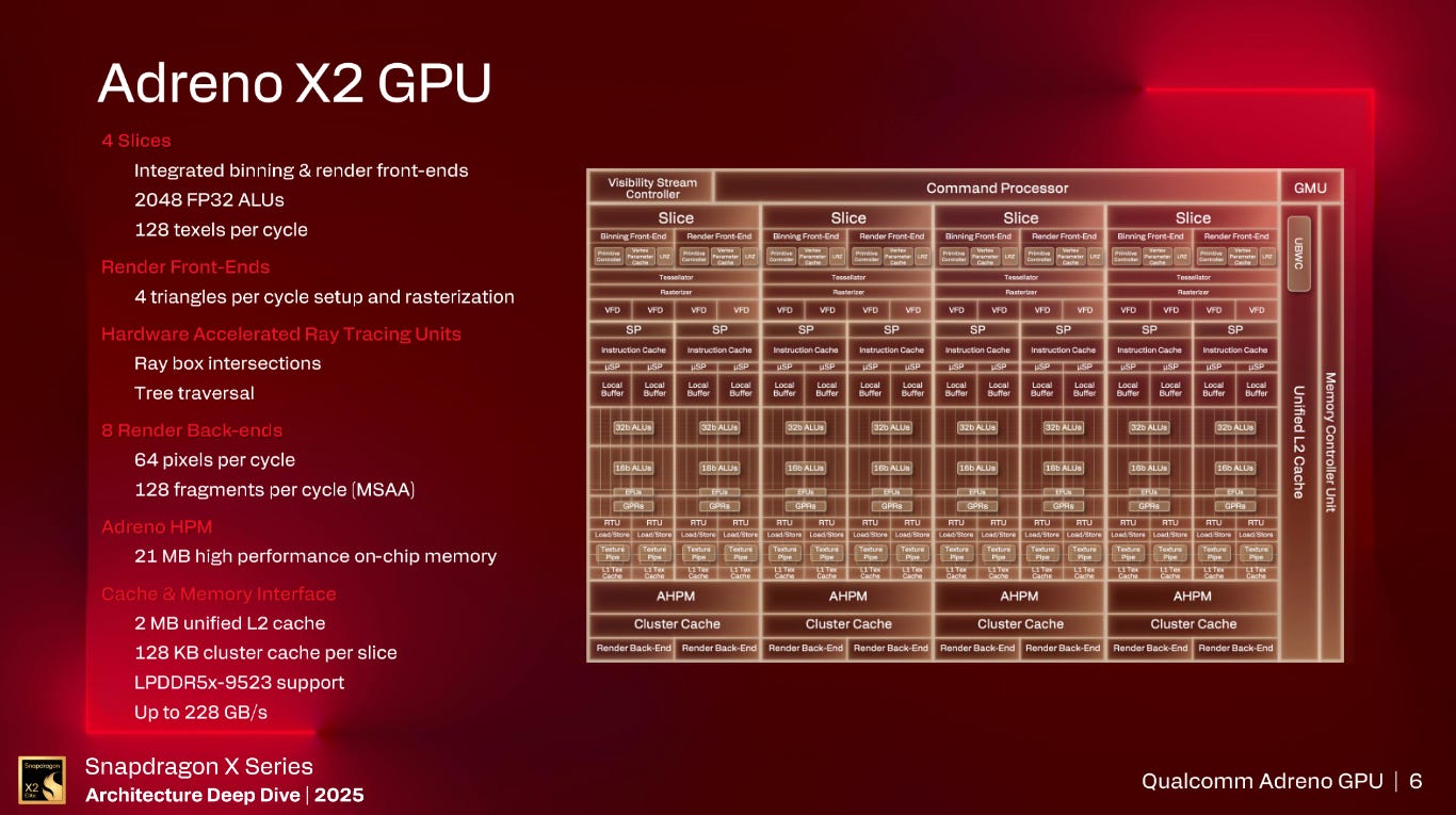
This is Qualcomm’s largest GPU they have made to date with 2048 FP32 ALUs clocking up to 1.85GHz.
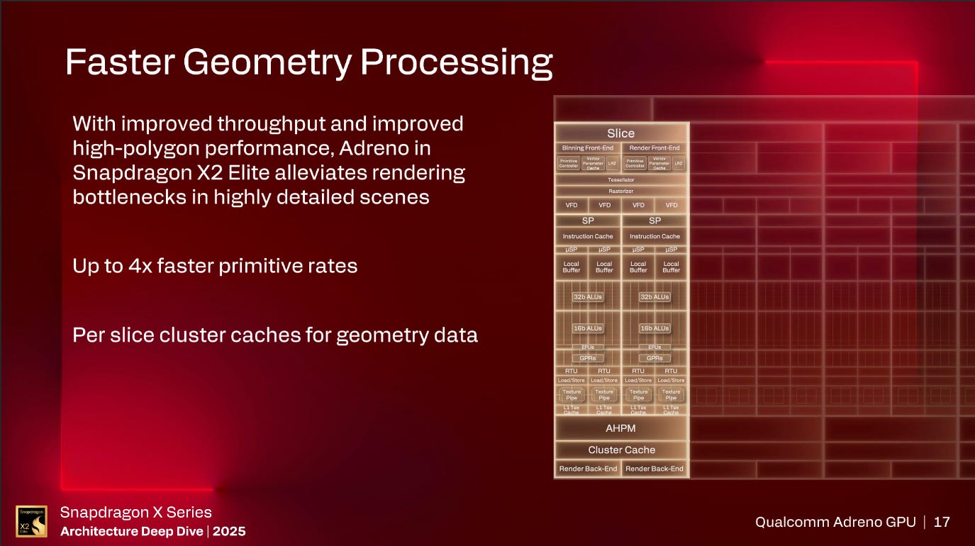
The Adreno X2 is a “Slice-Based” architecture, roughly equivalent to a Shader Engine from AMD or a GPC from Nvidia, with 4 slices for the top-end X2-90. Each slice has one Front-End which capable of rasterizing up to 4 triangles per cycle.
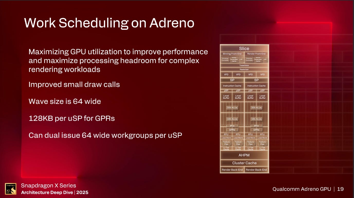
After the Front-end, are the Shader Processors, which are roughly equivalent to AMD’s WGP or Nvidia’s SM, which has an instruction cache and 2 micro-Shader Processors (uSP), similar to AMD’s SIMD unit or Nvidia’s SMSP, which each have a 128KB register file feeding 128 ALUs which support FP32, FP16, and BF16. A change from the prior Adreno X1 architecture is the removal of Wave128, now the Adreno X2 only supports Wave64 and can dual issue Wave64 instructions in order to keep the 128 ALUs fed.
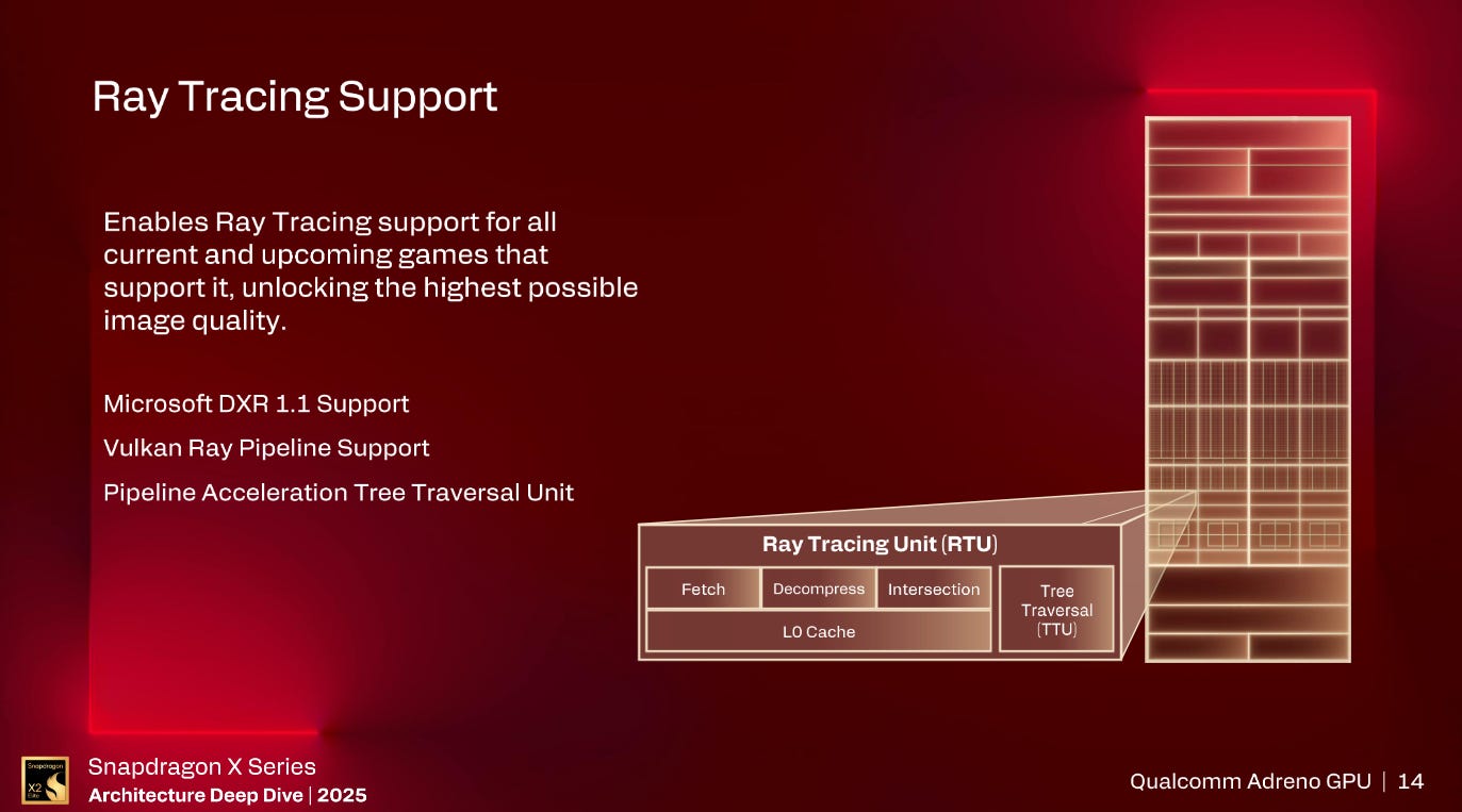
Each uSP has a Ray Tracing Unit which supports either 4 ray-triangles or 8 ray-box intersections per cycle.
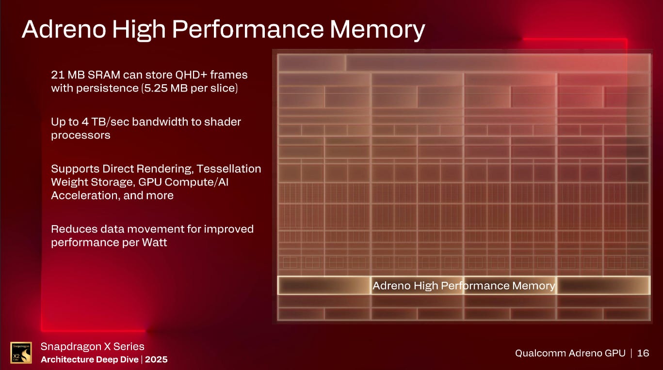
From there is what is referred to as Adreno High Performance Memory (AHPM). There is 21 MB of AHPM in a X2-90 GPU, 5.25 MB per slice, which is both a scratchpad and a cache depending on what the driver configures it as. Up to 3 MB of each of the 5.25 MB slices can be configured as a cache with the remaining 2.25 MB of SRAM being a scratchpad.
AHPM is designed to allow for the GPU to do tiled rendering all within the AHPM before rendering out the frame to the display buffer. This reduces the amount of data movement that the GPU has to do which consequently improves the performance per watt of the Adreno X2 compared to the Adreno X1.
Moving back to the Slice level, each slice has a 128 KB cluster cache which is then backed by a unified 2 MB L2 cache. This L2 can then spill into the 8 MB System Level Cache (SLC) which then is backed by the up to 228 GB/s memory subsystem.
As for API support, Adreno X2 supports DX12.2, Shader Model 6.8, Vulkan 1.4, OpenCL 3.0, as well as SYCL support coming in the first half of 2026.
Hexagon NPU
Qualcomm has increased the performance of the Hexagon NPU from 45 TOPS of INT8 to 80 TOPS of INT8 with SDX2E.

Qualcomm has also added FP8 and BF16 support to the Hexagon NPU 6 vector unit.

In addition to the BF16 and FP8 support, the new matrix engine in NPU 6 has INT2 dequantization support.

However, the largest change in NPU 6 is the addition of 64 bit Virtual Addressing to the DMA unit which means that NPU 6 can now access more than 4GB of memory.

Power and Performance
For testing the power of a system, Qualcomm has used what they call INPP or Idle Normalized Platform Power. What INPP is, is talking the total platform power during load and subtracting out the platform power at idle.
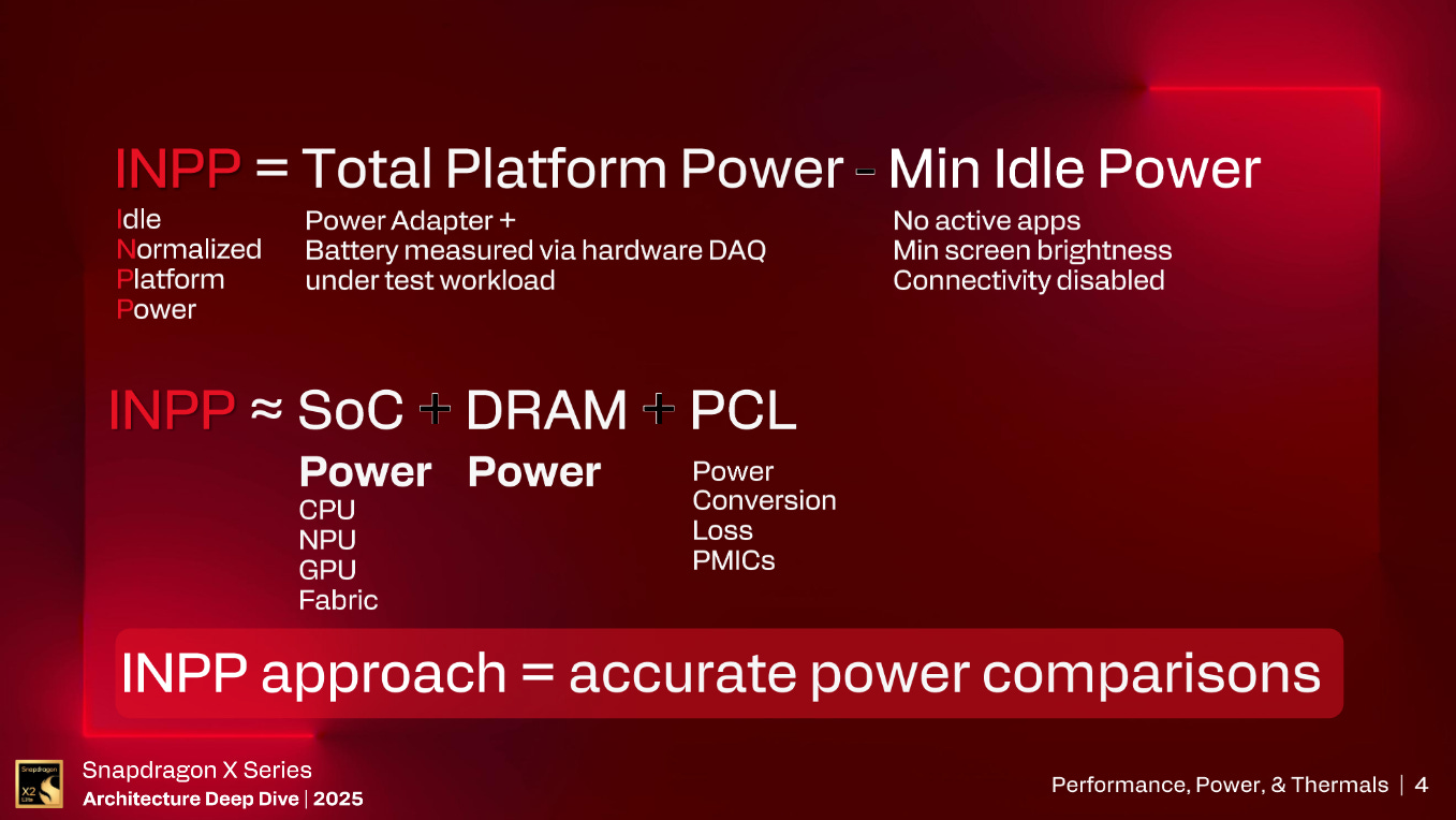
What INPP gets you is the SOC power plus the DRAM power plus the Power Conversion Losses; while this isn’t quite solely SOC power, INPP is about as close as you can get to pure SOC power in a laptop form factor where discrete power sensors aren’t very common.
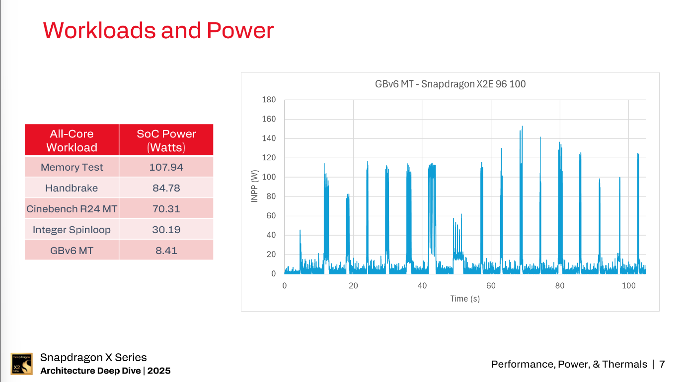
Different workloads have different power characteristics. For example, while GB 6 Multi-threaded doesn’t pull a ton of power overall, it is a very bursty workload that can spike to over 150 watts; whereas a memory bandwidth test pulls over 105 watts in a sustained fashion.
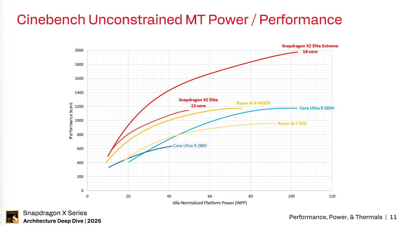
Looking at the performance versus power graph in Cinebench R24 MT, the SDX2E Extreme with 18 cores (12 Prime and 6 Performance cores) scores just over 1950 points in Cinebench R24 at about 105 watts INPP with the standard SDX2E with 12 cores (6 Prime and 6 Performance cores) scoring just over 1100 points at approximately 50 watts INPP.
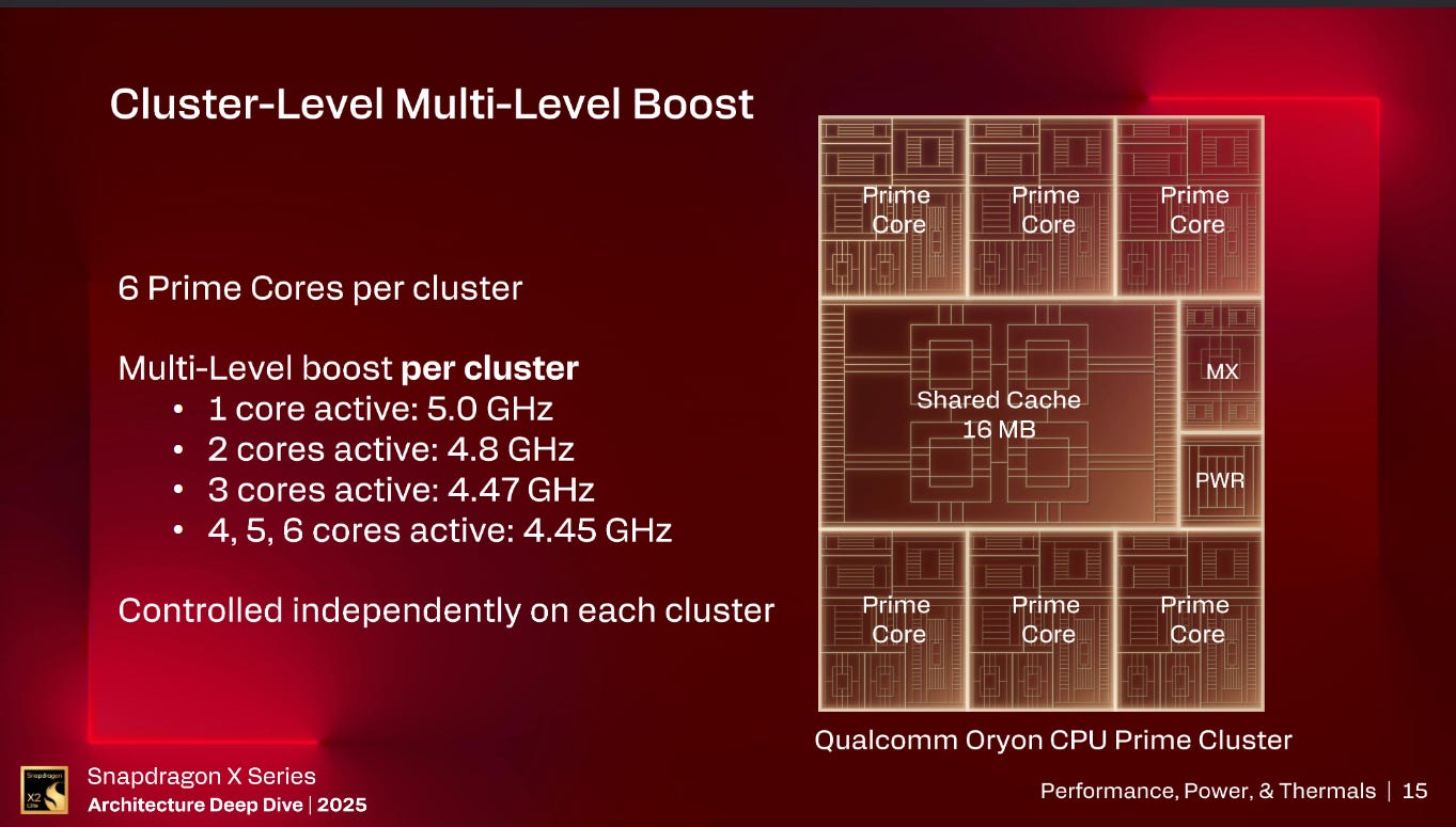
Qualcomm has also implemented a clock boosting scheme similar to Intel’s Turbo Boost where depending on the number of cores active in a cluster, the cluster will clock up or down accordingly.
Editor’s Note (11/30/2025): Qualcomm got in touch with Chips and Cheese to clarify that their boosting algorithm is a cluster-level algorithm where the boosting behavior is independent for the 3 clusters; where as Intel’s Turbo Boost mechanism is a SoC-level algorithm that affects all cores on the package.
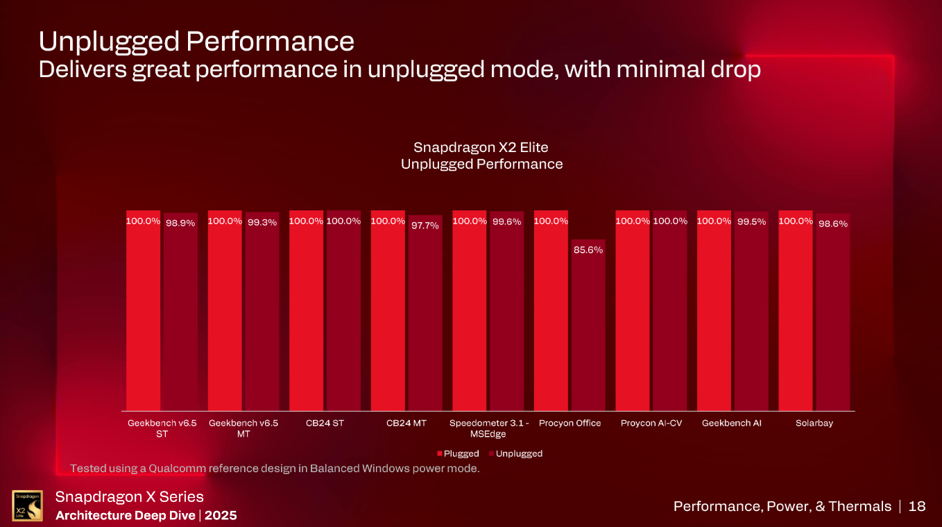
Qualcomm also highlighted the performance of the SDX2E when the laptop is on battery performance compared to the laptop on wall power.
Conclusion
Qualcomm has made significant advances with the SDX2E with regards to the SOC, GPU, and NPU. SDX2E is planned to hit shelves in the first half of 2026 and we can’t wait to get a system to test.
If you like the content then consider heading over to the Patreon or PayPal if you want to toss a few bucks to Chips and Cheese. Also consider joining the Discord.
Qualcomm calling their efficiency cores "Performance" cores, while also coming in at only six vs the "Prime" core count of 12 is not confusing at all!
Qualcomm "Performance" cores = Every other chipmaker's efficiency cores
Qualcomm "Prime" cores = Every other chipmaker's performance cores.
Also, there's spelling mistakes in the Qualcomm slides. Very professional.
How you guys comprehend this stuff amazes me.