
Qualcomm's Centriq 2400 and the Falkor Architecture

Cloud computing rose rapidly around 2010, powered by AMD’s Opteron and Intel’s Xeon processors. The large cloud market piqued the interest of other CPU makers including Qualcomm. Qualcomm had grown to become a formidable force in the mobile SoC market by the mid-2010s, and had several in-house CPU designs under their belt. They had good reason to be confident about their cloud server prospects. High core counts in server chips translate to low per-core power, blunting AMD and Intel’s greatest strength of high single threaded performance.

Meanwhile, Qualcomm’s mobile background gave them plenty of experience in low power CPU design. Their high mobile volume gave them access to Samsung’s 10nm FinFET process. That could at least level the playing field against Intel’s 14nm node, if not give Qualcomm an outright advantage in power consumption and density. Qualcomm hoped to use those factors to deliver a cheaper, lower power competitor on the cloud computing scene.
To break into the cloud computing segment, Qualcomm needed a CPU architecture with enough performance to meet key metrics in areas like tail-end latency. During a Hot Chips presentation, Qualcomm noted that throwing a pile of weak cores onto a chip and calling it day wouldn’t cut it. An Arm cloud CPU may not have to match Intel and AMD core for core, but they do need to hit a baseline level of performance. Qualcomm hopes to do that while maintaining their traditional power and density advantages.
Core Overview
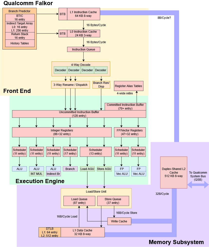
The Falkor CPU architecture aims to meet that performance threshold with low power and silicon area requirements. Falkor is a 4-wide aarch64 core with features inherited from Qualcomm’s prior mobile cores. It runs the 64-bit Arm instruction set (aarch64, armv8) with a few features pulled in from armv8.1. 32-bit Arm support is absent, as there’s no large existing install base of Arm server applications. Falkor is Qualcomm’s 5th in-house core design, and the company’s first designed specifically for cloud computing.
A Centriq 2400 series chip packs up to 48 Falkor cores on a 398mm2 die with a 120W TDP. That translates to less than 2.5W per core. Qualcomm notes that power consumption is usually well under 120W in typical all-core loads.

For this article, Neggles (Andi) was given a Centriq 2452 system from the folks at Corellium at no cost in order for us to test it. So a massive shout out to both Corellium for providing the system as well as to Neggles for getting the system up and running.
The Centriq 2452 system is set up with 96 GB of DDR4 running at 2666 MT/s, and identifies itself as the “Qualcomm Centriq 2400 Reference Evaluation Platform CV90-LA115-P23”.
Frontend
Falkor has both a L0 and L1 instruction cache like Qualcomm’s prior Krait architecture, and possibly Kryo too. The 24 KB, 3-way set associative L0 delivers instructions at lower power and with lower latency. The L0 is sized to contain the large majority of instruction fetches, while the 64 KB 8-way L1 instruction cache handles larger code footprints. Although the L0 fills a similar role to micro-op caches and loop buffers in other CPUs, it holds ISA instruction bytes just like a conventional instruction cache.
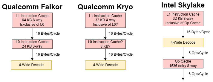
Both instruction cache levels have enough bandwidth to feed Falkor’s 4-wide decoder. The two instruction cache levels are exclusive of each other, so the core effectively has 88 KB of instruction cache capacity. Qualcomm might use a victim cache setup to maintain that exclusive relationship. If so, incoming probes would have to check both the L0 and L1, and L1 accesses would incur the additional cost of a copy-back from L0 on top of a fill into L0. An inclusive setup would let the L1 act as a snoop filter for the L0 and reduces the cost of L1 accesses, but has less total caching capacity.
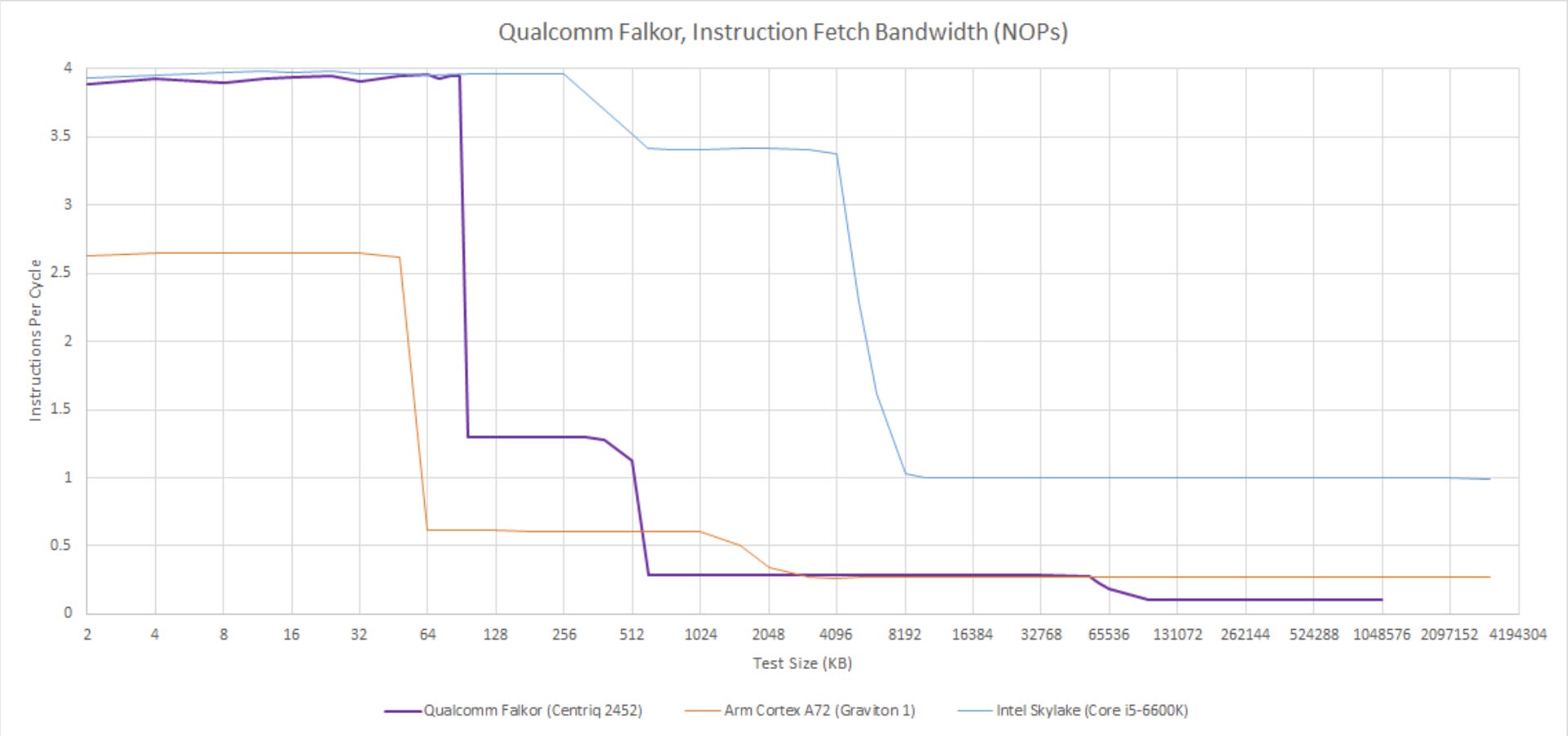
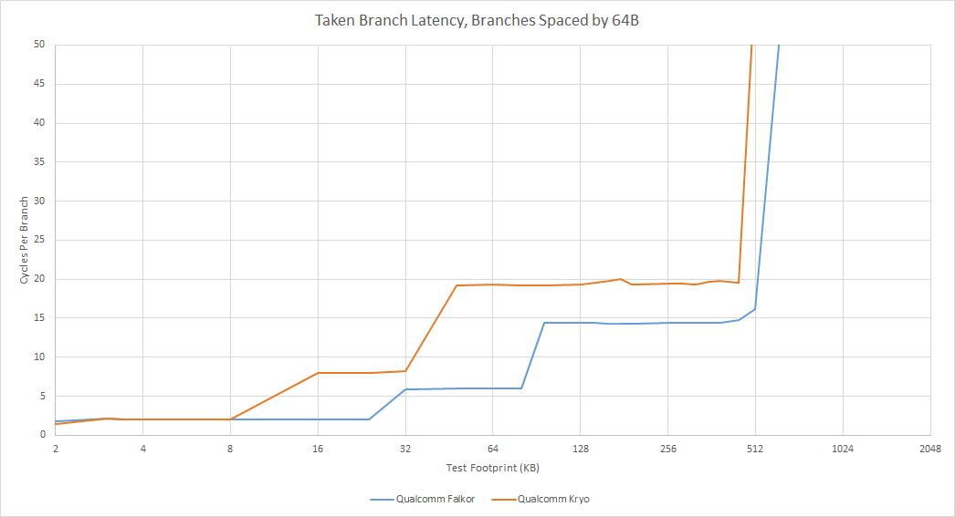
The exclusive L0/L1 setup gives Falkor high instruction caching capacity compared to contemporary cores. Falkor wouldn't be beaten in this respect until Apple's M1 launched several years later. High instruction cache capacity makes L2 code fetch bandwidth less important. Like many 64-bit Arm cores of the time, or indeed AMD's pre-Zen cores, Falkor's instruction throughput drops sharply once code spills into L2. Still, Faklor performs better than A72 in that respect.
Falkor's instruction caches are parity protected, as is common for many CPUs. Hardware resolves parity errors by invalidating corrupted lines and reloading them from L2. The instruction caches also hold branch targets alongside instruction bytes, and therefore serve as branch target buffers (BTBs). A single cache access provides both instructions and branch targets, so Falkor doesn't have to make a separate BTB access like cores with a decoupled BTB do. However, that prevents the branch predictor from following the instruction stream past a L1i miss.
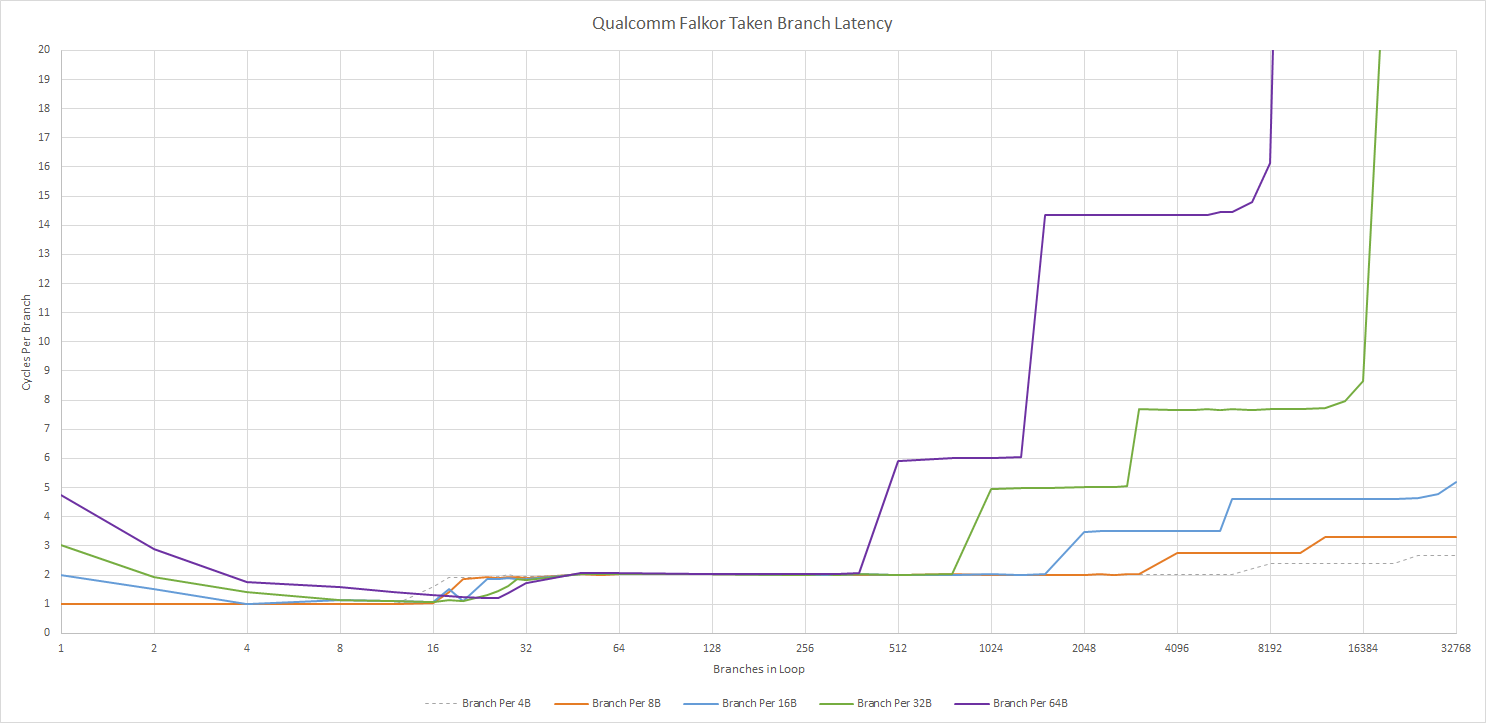
Taken branches incur one pipeline bubble (2 cycle latency) within L0, and up to 6 cycle latency from L1. For smaller branch footprints, Falkor do zero-bubble taken branches using a 16 entry branch target instruction cache (BTIC). Unlike a BTB, the BTIC caches instructions at the branch destination rather than the target address. It therefore bypasses cache latency, and allows zero-bubble taken branches without needing to make a L0 achieve single cycle latency.
Direction prediction uses multiple history tables, each using a different history length. The branch predictor tracks which history length and corresponding table works best for a given branch. The scheme described by Qualcomm is conceptually similar to a TAGE predictor, which also uses multiple history tables and tags tables to indicate whether they’re useful for a given branch. Falkor doesn’t necessarily use a classic TAGE predictor. For example, the history lengths may not be in a geometric series. But the idea of economizing history storage by using the most appropriate history length for each branch still stands. Arm’s Cortex A72 uses a 2-level predictor, presumably with a single table and a fixed history length.

In an abstract test with varying numbers of branches, each being taken or not-taken in random patterns of increasing length, Falkor does slightly better than Kryo. Falkor handles better with a lot of branches in play, though the longest repeating pattern either core can handle is similar for a small number of branches.

Falkor a two-level indirect target array for indirect branches, which read a target from a register rather than specifying a jump distance. An indirect branch may go to different targets, adding another dimension of difficulty to branch prediction. Falkor’s first level indirect target array has 16 entries, while a second level has 512 entries.

Having multiple targets for an indirect branch carries little penalty as long as total target count doesn’t exceed 16. That can be one branch switching between 16 targets, or eight branches alternating between two targets each.
Returns are a special case of indirect branches, because they typically go back to the call site. Falkor has a 16 entry return stack like Kryo. Cortex A72 has a much larger return stack with 31 entries. A function call and return costs approximately four cycles on Falkor, Kryo, and A72, which would be an average of 2 cycles per branch-with-link instruction.

Falkor’s decoders translate up to four instructions per cycle into micro-ops. Like most other CPUs, Qualcomm aims to decode most common instructions into a single micro-op. 128-bit vector math instructions appear to be a notable exception.
Rename/Allocate
Micro-ops from the decoders need resources allocated in the backend for bookkeeping during out-of-order execution. Falkor’s renamer can handle register renaming and resource allocation for up to for micro-ops per cycle. However, the fourth slot can only process direct branches and a few specialized cases like NOPs or recognized register zeroing cases. A conditional branch that also includes an ALU operation, like cbz/cbnz, cannot go into the fourth slot.
Besides special handling for zeroing registers by moving an immediate value of zero into it, I didn’t see other common optimizations carried out.There’s no MOV elimination, and the renamer doesn’t recognize that XOR-ing or subtracting a register from itself results in zero.
Out-of-Order Execution
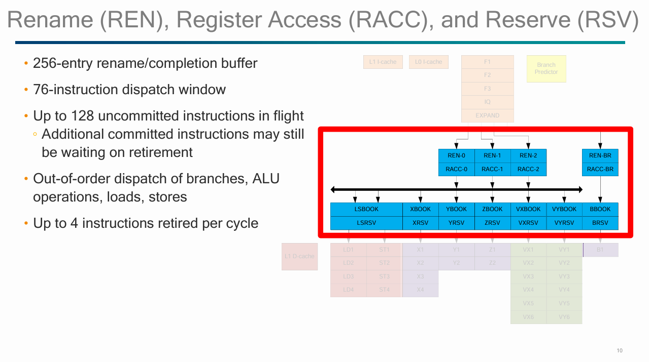
Falkor doesn’t have a classic reorder buffer, or ROB. Rather, it uses a series of structures that together enable out-of-order execution while ensuring program results are consistent with in-order execution. Falkor has a 256 entry rename/completion buffer. Qualcomm further states Falkor can have 128 uncommitted instructions in flight, along with another 70+ uncommitted instructions for a total of 190 in-flight instructions. The core can retire 4 instructions per cycle.
From a microbenchmarking perspective, Falkor acts like Arm’s Cortex A73. It can free resources like registers and load/store queue entries past a long latency load, with no visible limit to reordering capacity even past 256 instructions. An unresolved branch similarly blocks out-of-order resource deallocation, after which Falkor’s reordering window can be measured. At that point, I may be measuring what Qualcomm considers uncommitted instructions.

Kryo and Falkor have similar reordering capacity from that uncommitted instruction perspective. But otherwise Qualcomm has re-balanced the execution engine to favor consistent performance for non-vector code. Falkor has a few more register file entries than Kryo, and more crucially, far larger memory ordering queues.

Integer execution pipelines on Falkor are specialized to handle different categories of operations from each other. Three pipes have integer ALUs, and a fourth pipe is dedicated to direct branches. Indirect branches use one of the ALU ports. Another ALU port has an integer multiplier, which can complete one 64-bit multiply per cycle with 5 cycle latency. Each ALU pipe has a modestly sized scheduler with about 11 entries.
Falkor has two largely symmetric FP/vector pipelines, each also with a 11 entry scheduler. Both pipes can handle basic operations like FP adds, multiplies, and fused multiply-adds. Vector integer adds and multiplies can also execute down both pipes. More specialized operations like AES acceleration instructions are only supported by one pipe.
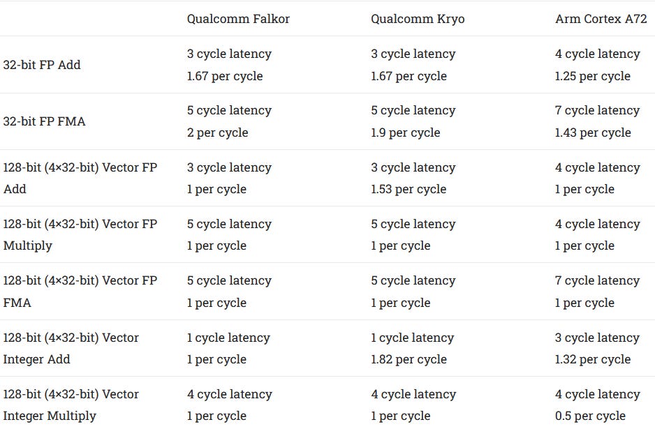
FP and vector execution latency is similar to Kryo, as is throughput for scalar FP operations. Both of Falkor’s FP/vector pipes have a throughput of 64 bits per cycle. 128-bit math instructions are broken into two micro-ops, as they take two entries in the schedulers, register file, and completion buffer. Both factors cut into potential gains from vectorized code.
Memory Access
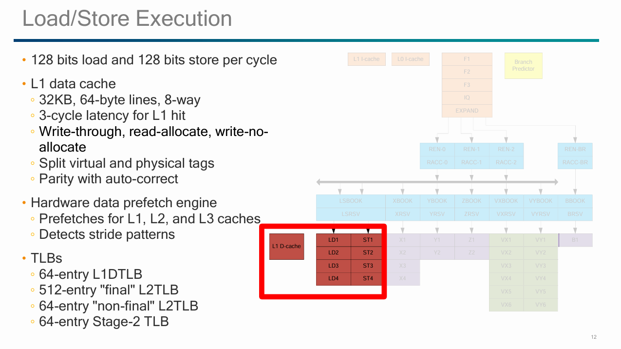
Falkor’s load/store subsystem is designed to handle one load and one store per cycle. The memory pipeline starts with a pair of AGUs, one for loads and one for stores. Both AGUs are fed from a unified scheduler with approximately 13 entries. Load-to-use latency is 3 cycles for a L1D hit, and the load AGU can handle indexed addressing with no penalty.
Virtual addresses (VAs) from the load AGU proceeds to access the 32 KB 8-way L1 data cache, which can provide 16 bytes per cycle. From testing, Falkor can handle either a single 128-bit load or store per cycle, or a 64-bit load and a 64-bit store in the same cycle. Mixing 128-bit loads and stores does not bring throughput over 128 bits per cycle.
Every location in the cache has a virtual tag and a physical tag associated with it… If you don’t have to do a TLB lookup prior to your cache, you can get the data out faster, and you can return the data with better latency.
Qualcomm’s Hot Chips 29 presentation
The L1D is both virtually and physically tagged, which lets Falkor retrieve data from the L1D without waiting for address translation. A conventional VIPT (virtually indexed, physically tagged) cache could select a set of lines using the virtual address, but needs the physical address (PA) to be available before checking tags for hits Qualcomm says some loads can skip address translation completely, in which case there’s no need for loads to check the physical tags at all. It’s quite an interesting setup, and I wonder how it handles multiple VAs aliasing to the same PA.
…a novel structure that is built off to the side of the L1 data cache, that acts almost like a write-back cache. It’s a combination of a store buffer, a load fill buffer, and a snoop filter buffer from the L2, and so this structure that sits off to the side gives us all the performance benefit and power savings of having a write-back cache without the need for the L1 data cache to be truly write-back
Qualcomm’s Hot Chips 29 presentation
Falkor’s store pipeline doesn’t check tags at all. The core has a write-through L1D, and uses an unnamed structure to provide the power and performance benefits of a write-back L1D. It functionally sounds similar to Bulldozer’s Write Coalescing Cache (WCC), so in absence of a better name from Qualcomm, I’ll call it that. Multiple writes to the same cacheline are combined at the WCC, reducing L2 accesses.
Stores on Falkor access the L1D physical tags to ensure coherency, and do so after they’ve reached the WCC. Thus the store combining mechanism also serves to reduce physical tag checks, saving power.

Qualcomm is certainly justified in saying they can deliver the performance of a write-back cache. A Falkor core can’t write more than 16B/cycle, and the L2 appears to have for more bandwidth than that. One way to see the WCC is to make one store per 128B cacheline, which reveals it’s a 3 KB per-core structure and can write a 128B cacheline back to L2 once every 2-3 cycles. But software shouldn’t run into this in practice.

Other architectures that use a write-through L1D, notably Intel’s Pentium 4 and AMD’s Bulldozer, suffered from poor store forwarding performance. Falkor doesn’t do well in this area, but isn’t terrible either. Loads that are 32-bit aligned within a store that they depend on can get their data with 8 cycle latency (so possibly 4 cycles for the store, and four cycles for the load). Slower cases, including partial overlaps, are handled with just one extra cycle. I suspect most cores handle partial overlaps by waiting for the store to commit, then having the load read data from cache. Quaclomm may have given Falkor a more advanced forwarding mechanism to avoid the penalty of reading from the WCC.
Using a write-through L1D lets Qualcomm parity protect the L1D rather than needing ECC. As with the instruction caches, hardware resolves parity errors by reloading lines from lower level caches, which are ECC protected.
Address Translation
Unlike mobile cores, server cores may encounter large data footprints with workloads running inside virtual machines. Virtualization can dramatically increase address translation overhead, as program-visible VAs are translated to VM-visible PAs, which in turn are translated via hypervisor page tables to a host PA. A TLB miss could require walking two sets of paging structures, turning a single memory access into over a dozen accesses under the hood.

Kryo appears to have a single level 192 entry TLB, which is plainly unsuited to such server demands. Falkor ditches that all-or-nothing approach in favor of a more conventional two-level TLB setup. A 64 entry L1 DTLB is backed by a 512 entry L2 TLB. Getting a translation from the L2 TLB adds just two cycles of latency, making it reasonably fast. Both the L1 DTLB and L2 TLB store “final” translations, which map a program’s virtual address all the way to a physical address on the host.
Falkor also has a 64 entry “non-final” TLB, which caches a pointer to the last level paging structure and can skip much of the page walk. Another “stage-2” TLB with 64 entries caches translations from VM PAs to host PAs.
System Architecture
Server chips must support high core counts and high IO bandwidth, which is another sharp difference between server and mobile SoCs. Qualcomm implements Falkor cores in dual core clusters called duplexes, and uses that as a basic building block for their Centriq server SoC. Kryo also used dual core clusters with a shared L2, so that concept isn’t entirely alien to Qualcomm.
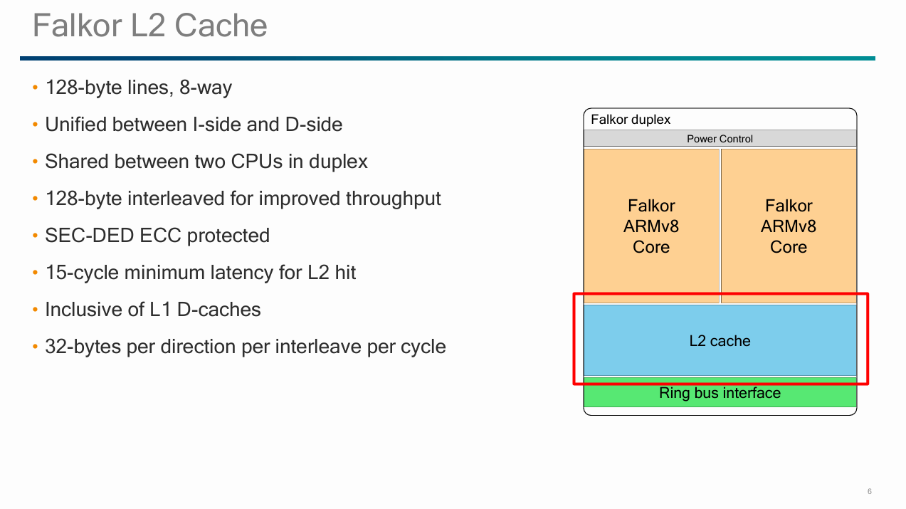
Falkor’s L2 is a 512 KB, 8-way set associative, and inclusive of L1 contents. It serves both as a mid-level cache between L1 and the on-chip network, as well as a snoop filter for the L2 caches. The L2 is ECC protected, because it can contain modified data that hasn’t been written back anywhere else.
Qualcomm says the L2 has 15 cycles of latency, though a pointer chasing pattern sees 16-17 cycles of latency. Either way, it’s a welcome improvement over Kryo’s 20+ cycle L2 latency. Kryo and Arm’s Cortex A72 used the L2 as a last-level cache, which gave them the difficult task of keeping latency low enough to handle L1 misses with decent performance, while also having enough capacity to insulate the cores from DRAM latency. A72 uses a 4 MB L2 cache with 21 cycle latency, while Kryo drops the ball with both high latency and low L2 capacity.

Multiple interleaves (i.e. banks) help increase L2 bandwidth. Qualcomm did not specify the number of interleaves, but did say each interleave can deliver 32 bytes per cycle. The L2 appears capable of handling a 128B writeback every cycle, so it likely has at least four interleaves. Two Falkor cores in a complex together have just 32B/cycle of load/store bandwidth, so the L2 has more than enough bandwidth to feed both cores. In contrast, the L2 caches on Kryo and A72 have noticeably less bandwidth than their L1 caches.
A Falkor duplex interfaces with the system using the Qualcomm System Bus (QSB) protocol. QSB is a proprietary protocol that fulfills the same function as the ACE protocol used by Arm. It can also be compared to Intel’s IDI or AMD’s Infinity Fabric protocols. The duplex’s system bus interface provides 32 bytes per cycle of bandwidth per direction, per 128B interleave.
On-Chip Network
Qualcomm uses a bidirectional, segmented ring bus to link cores, L3 cache, and IO controllers. Data transfer uses two sets of bidirectional rings, and traffic is interleaved between the two bidirectional rings at 128B cacheline granularity. In total, Centriq has four rings covering even and odd interleaves in both clockwise and counterclockwise directions. Qualcomm’s slides suggest each ring can move 32B/cycle, so the ring bus effectively has 64B/cycle of bandwidth in each direction.

A dual core cluster can access just under 64 GB/s of L3 bandwidth from a simple bandwidth test, giving Qualcomm a significant cache bandwidth advantage over Cortex A72. L3 bandwidth from a dual core Falkor complex is similar to that of a Skylake core on the Core i5-6600K.

Ring bus clients include up to 24 dual core clusters, 12 L3 cache slices, six DDR4 controller channels, six PCIe controllers handling 32 Gen 3 lanes, and a variety of low speed IO controllers.
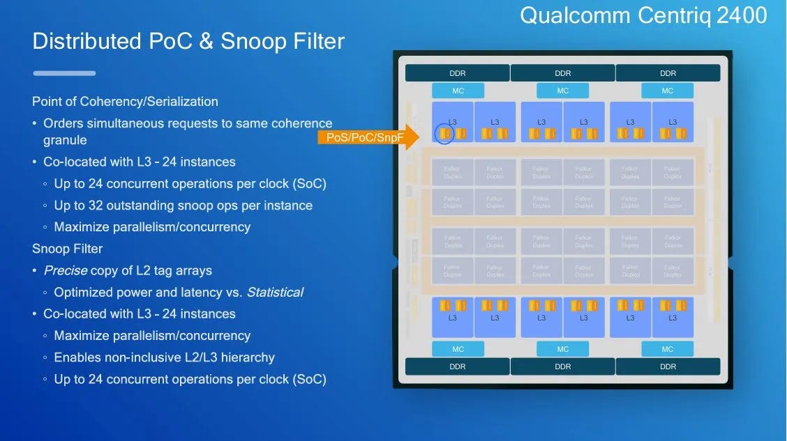
L3 Cache
Centriq’s L3 slices have 5 MB of capacity and are 20-way set associative, giving the chip 60 MB of total L3 capacity across the 12 slices. The 46 core Centriq 2452 has 57.5 MB enabled. Cache ways can be reserved to divide L3 capacity across different applications and request types, which helps ensure quality of service.

Addresses are hashed across L3 slices to enable bandwidth scalability, like many other designs with many cores sharing a large L3. Centriq doesn’t match L3 slice count to core count, unlike Intel and AMD designs. However, each Centriq L3 slice has two ring bus ports, so the L3 and Falkor duplexes the same aggregate bandwidth to the on-chip network.
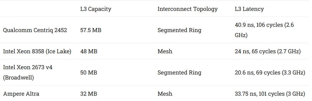
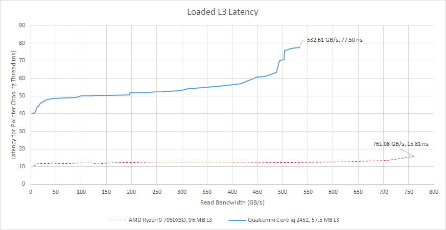
L3 latency is high at over 40 ns, or north of 100 cycles. That’s heavy for cores with 512 KB of L2. Bandwidth can scale to over 500 GB/s, which is likely adequate for anything except very bandwidth heavy vector workloads. Falkor isn’t a great choice for vector workloads anyway, so Centriq has plenty of L3 bandwidth. Latency increases to about 50 ns under moderate bandwidth load, and reaches 70-80 ns when approaching L3 bandwidth limits. Contention from loading all duplexes can bring latency to just over 90 ns.
Centriq’s L3 also acts as a point of coherency across the chip. The L3 is not inclusive of the upper level caches, and maintains L2 snoop filters to ensure coherency. In that respect it works like the L3 on AMD’s Zen or Intel’s Skylake server. Each L3 slice can track up to 32 outstanding snoops. Cache coherency operations between cores in the same duplex don’t need to transit the ring bus.

A core to core latency test shows lower latency between core pairs in a duplex, though latency is still high in an absolute sense. It also indicates Qualcomm has disabled two cores on the Centriq 2452 by turning off one core in a pair of duplexes. Doing so is a slightly higher performance option because two cores don’t have to share L2 capacity and a system bus interface.
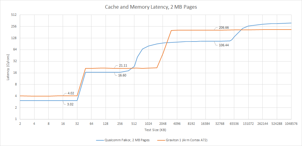
Centriq supports up to 768 GB of DDR4 across six channels. The memory controllers support speeds of up to 2666 MT/s for 128 GB/s of theoretical bandwidth. Memory latency is about 121.4 ns, and is poorly controlled under high bandwidth load. Latency can rise beyond 500 ns at over 100 GB/s of bandwidth usage. For comparison, Intel is able to keep latency below 200 ns with more than 90% bandwidth utilization. Still, Centriq has plenty of bandwidth from an absolute sense. Against contemporary Arm server competition like Amazon’s Graviton 1, Centriq has a huge bandwidth advantage. Furthermore, the large L3 should reduce DRAM bandwidth demands compared to Graviton 1.

Unlike Intel and AMD server processors, Centriq cannot scale to multi-socket configurations. That caps a Centriq server to 48 cores, while AMD’s Zen 1 and Intel’s Skylake can scale further using multiple sockets. Qualcomm’s decision to not pursue multi-socket reasons is reasonable, because cross-socket connections require both massive bandwidth and additional interconnect work. However, it does exclude more specialized cloud applications that benefit from VMs with over a hundred CPU cores and terabytes of memory. Having just 32 PCIe lanes also limits Centriq’s ability to host piles of accelerators. Even contemporary high end workstations had more PCIe lanes.
Thus Centriq’s system architecture is designed to tackle mainstream cloud applications, rather than trying to cover everything Intel does. By not tackling all those specialized applications, Qualcomm’s datacenter effort can avoid getting distracted and focus on doing the best job they can for common cloud scenarios. For those use cases, sticking with 32 PCIe lanes and integrating traditional southbridge functions like USB and SATA likely reduce platform cost. And while Centriq’s interconnect may not compare well to Intel’s, it’s worlds ahead of Graviton 1.
Performance
In SPEC CPU2017, a Falkor core comfortably outperforms Arm’s Cortex A72, with a 21.6% lead in the integer suite and a 53.4% lead in the floating point suite. It falls behind later Arm offerings on more advanced process nodes.

With SPEC CPU2017’s integer workloads, Falkor compares best in memory-bound workloads like 505.mcf and 502.gcc. Falkor pulls off a massive lead in several floating point subtests like 503.bwaves and 507.cactuBSSN, which inflates its overall lead in the floating point suite.
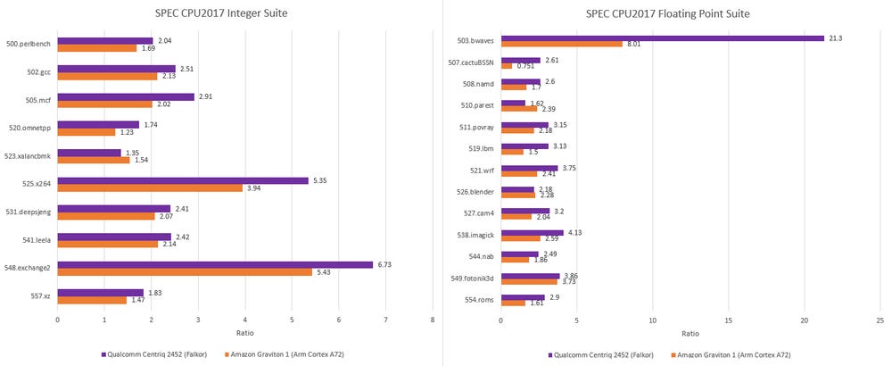
From an IPC perspective, Falkor is able to stretch its legs in cache-friendly workloads like 538.imagick. Yet not all high IPC workloads give Falkor a substantial lead. Cortex A72 is just barely behind in 548.exchange2 and 525.x264, two high IPC tests in SPEC CPU2017’s integer suite. It’s a reminder that Falkor is not quite 4-wide.

For comparison, I’ve included IPC figures from Skylake, a 4-wide core with no renamer slot restrictions. It’s able to push up to and past 3 IPC in easier workloads, unlike Falkor.
Quad Core Comparisons
With 7-Zip set to use eight threads and pinned to four cores, Falkor achieves a comfortable lead over Cortex A72. Using one core per cluster provides a negligible performance increase over loading both cores across two clusters.

Unlike 7-Zip, libx264 is a well vectorized workload. Falkor has poor vector capabilities, but so does Cortex A72. Again, additional L2 capacity from using four duplexes provides a slight performance increase. And again, Falkor has no trouble beating A72.
Final Words
Qualcomm’s Kryo mobile core combined high core throughput with a sub-par memory subsystem. Falkor takes a different approach in its attempt o break into the server market. Its core pipeline is a downgrade compared to Kryo in many respects. Falkor has fewer execution resources, less load/store bandwidth, and worse handling for 128-bit vectors. Its 3+1 renamer acts more as a replacement for branch fusion than making Falkor a truly 4-wide core, which is another step back from Kryo. Falkor improves in some respects, like being able to free resources out-of-order, but it lacks the raw throughput Kryo could bring to the table.
In exchange, Falkor gets a far stronger memory subsystem. It has more than twice as much instruction caching capacity. The load/store unit can track many more in-flight accesses and can perform faster store forwarding. Even difficult cases like partial load/store overlaps are handled well. Outside the core, Falkor’s L2 is much faster than Kryo’s, and L2 misses benefit from a 60 MB L3 behind a high bandwidth interconnect. Rather than spam execution units and core width, Qualcomm is trying to keep Falkor fed.

Likely, Falkor aims to deliver adequate performance across a wide variety of workloads, rather than exceptional performance on a few easy ones. Cutting back the core pipeline may also have been necessary to achieve Qualcomm’s density goals. 48 cores is a lot in 2017, and would have given Qualcomm a core count advantage over Intel and AMD in single socket servers. Doing so within a 120W envelope is even more impressive. Kryo was perhaps a bit too “fat” for that role. A wide pipeline and full 128-bit vector execution units take power. Data transfer can draw significant power too, and Kryo’s poor caching capacity did it no favors.
Falkor ends up being a strong contender in the 2017 Arm server market. Centriq walks all over Amazon’s Graviton 1, which was the first widely available Arm platform from a major cloud provider. Even with core cutbacks compared to Kryo, Falkor is still quite beefy compared to A72. Combined with a stronger memory subsystem, Falkor is able to beat A72 core for core, while having more cores on a chip.
But beating Graviton 1 isn’t enough. The Arm server scene wasn’t a great place to be around the late 2010s. Several attempts to make a density optimized Arm server CPU had come and gone. These included AMD’s “Seattle”, Ampere’s eMAG 8180, and Cavium’s ThunderX2. Likely, the strength of the x86-64 competition and nascent state of the Arm software ecosystem made it difficult for these early Arm server chips to break into the market. Against Skylake-X for example, Falkor is a much smaller core. Centriq’s memory subsystem is strong next to Kryo or A72’s, but against Skylake it has less L2 and higher L3 latency.
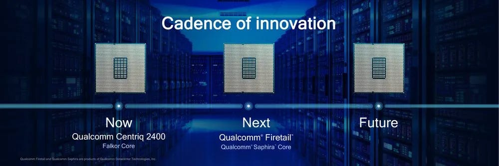
Qualcomm Datacenter Technologies no doubt accomplished a lot when developing the Centriq server SoC. Stitching together dozens of cores and shuffling hundreds of gigabytes per second across a chip is no small feat, and is a very different game from mobile SoC design. But taking on experienced players like Intel and AMD isn’t easy, even when targeting a specific segment like cloud computing. Arm would not truly gain a foothold in the server market until Ampere Altra came out after 2020. At that point, Arm’s stronger Neoverse N1 core and TSMC’s 7 nm FinFET process left Falkor behind. Qualcomm planned to follow up on Falkor with a “Saphira” core, but that never hit the market as far as I know.
However, Qualcomm is looking to make a comeback into the server market with their announcement of supplying HUMAIN, a Saudi state-backed AI company, with "datacenter CPUs and AI solutions". NVIDIA’s NVLink Fusion announcement also mentions Qualcomm as a provider of server CPUs that can be integrated with NVIDIA’s GPUs using NVLink. I look forward to seeing how that goes, and whether Qualcomm's next server CPU builds off experience gained with Centriq.
If you like the content then consider heading over to the Patreon or PayPal if you want to toss a few bucks to Chips and Cheese. Also consider joining the Discord.
Any thoughts on how Centriq's memory compression:
https://www.servethehome.com/qualcomm-centriq-2400-arm-cpu-hot-chips-29/qualcomm-centriq-2400-memory-bandwidth-compression/
affected latency? Is there a BIOS level toggle for this feature you could test?
I believe that one, maybe even the key reason for Falkor's failure to take off started with the prior lackluster commitment by Qualcomm to Open Source, namely Linux. That came to bite them in the butt when they tried to launch into a space (servers ) that is dominated by Linux. And Falkor faced a very different situation from Graviton and AWS. People at AWS didn't need to be convinced to adopt and push their homegrown ARM server CPU (Jeff Bezos would see to that). Convincing external customers to risk it and spend money on a new CPU Design (that's not x86/x64) was an uphill battle even with a good OS and software ecosystem in place. And as far as I remember, it wasn't.