
PEZY-SC4s at Hot Chips 2025
Continuing a supercomputing tradition with power efficient FP64 compute

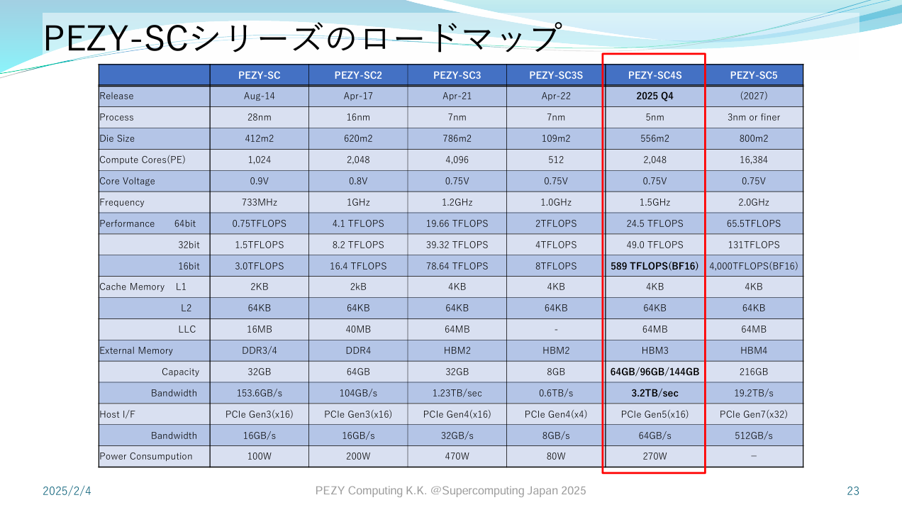
Japan has a long history of building domestic supercomputer architectures dating back to the 1980s. PEZY Computing is one player in Japan’s supercomputing scene alongside Fujitsu and NEC, and has taken several spots in the Green500 list. RIKEN’s Exascaler-1.4 used PEZY-SC chips to take first place in Green500’s November 2015 rankings. More recently, PEZY-SC3 placed 12th on Green500’s November 2021 list. PEZY presented their newest architecture, PEZY-SC4S, at Hot Chips 2025. While the physical product is not yet available, PEZY is presenting results of simulations and is talking about the architecture of SC4s.
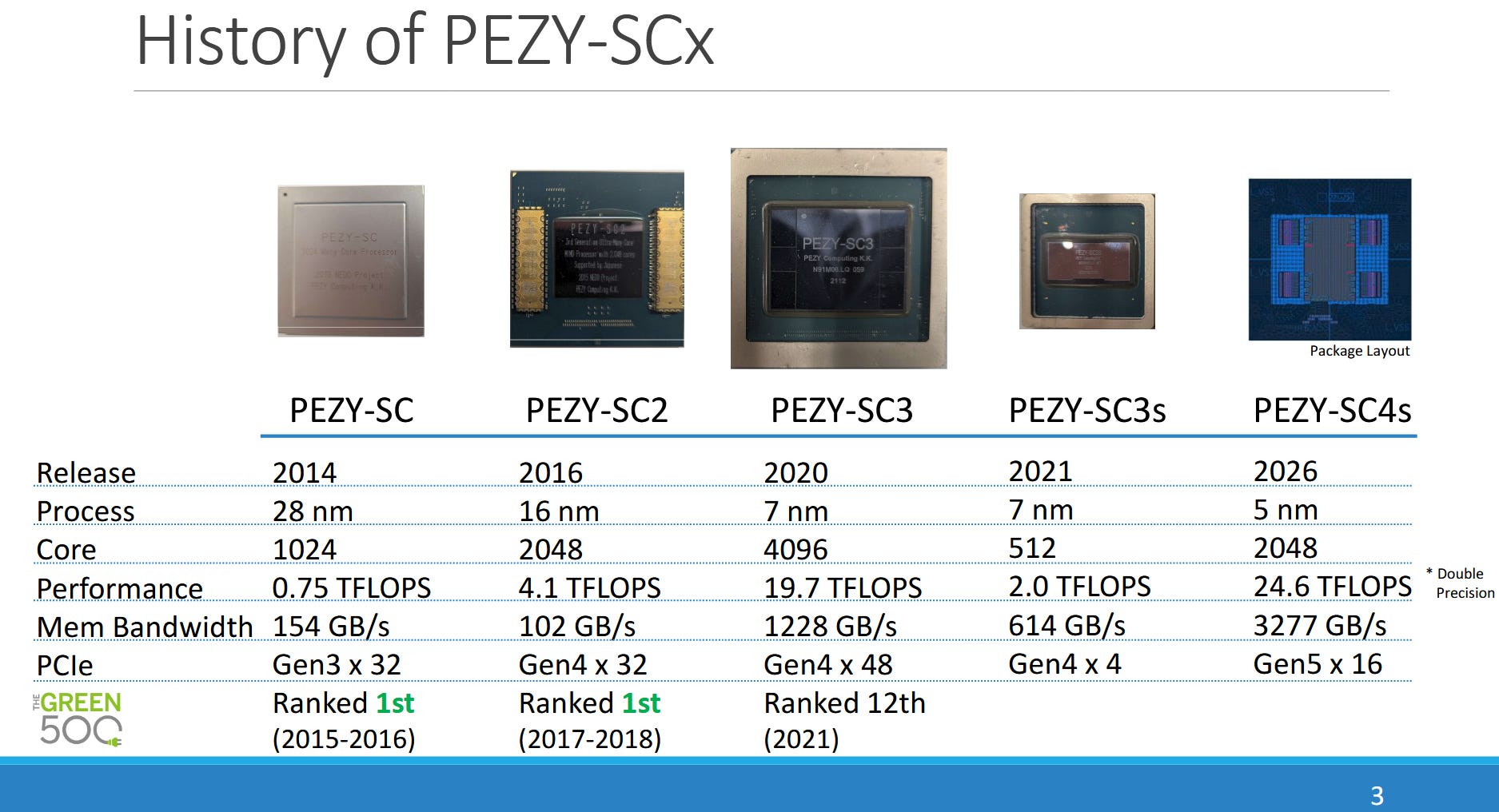
PEZY targets highly efficient FP64 compute by running a massively parallel array of execution units at lower clocks and voltages than contemporary GPUs. At the same time, it tries to avoid glass jaw performance behavior with low branching penalties and a sophisticated cache hierarchy. Their PEZY-SC products connect to a host system via PCIe, much like a GPU. The ‘s’ in SC4s denotes a scaled down model that uses a smaller die and draws less power. For example, PEZY-SC3 used a 786 mm2 die on TSMC’s 7nm process and drew up to 470W. PEZY-SC3s uses a smaller 109 mm2 die with a milder 80W power draw, and has 512 Processing Elements (PEs) compared to 4096 on the larger PEZY-SC3.
PEZY-SC4s is large for a ‘s’ part, with the same per-clock throughput as SC3. A bump from 1.2 to 1.5 GHz gives it a slight lead in overall throughput compared to SC3, and places it well ahead of SC3s.
SC4s’s Processing Element
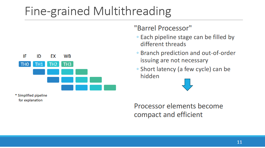
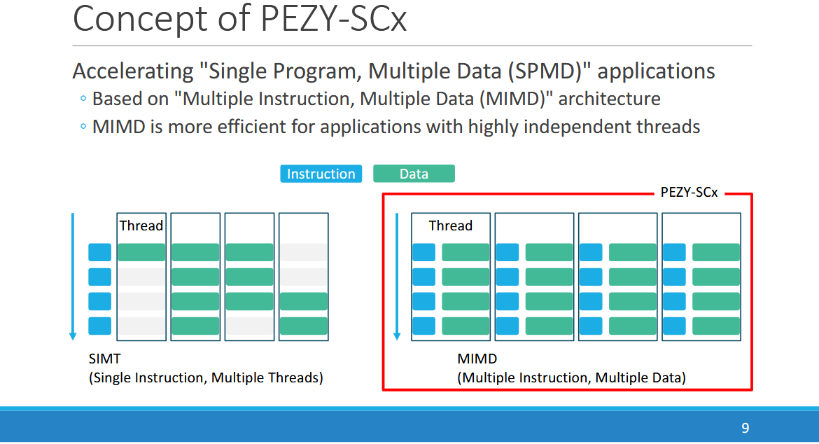
From an organization perspective, a PEZY PE is somewhat analogous to an execution unit partition on a GPU, like AMD’s SIMD or Nvidia’s SM sub-partitions. They’re very small cores that hide latency using thread level parallelism. On PEZY-SC4s, a PE has eight hardware threads, a bit like SMT8 on a CPU. These eight threads are arranged in pairs of “front” and “back” threads, but it’s probably more intuitive to see this is two groups of four threads. One four-thread group is active at a time. Hardware carries out fine-grained multithreading within a group, selecting a different thread every cycle to hide short duration stalls within individual threads.
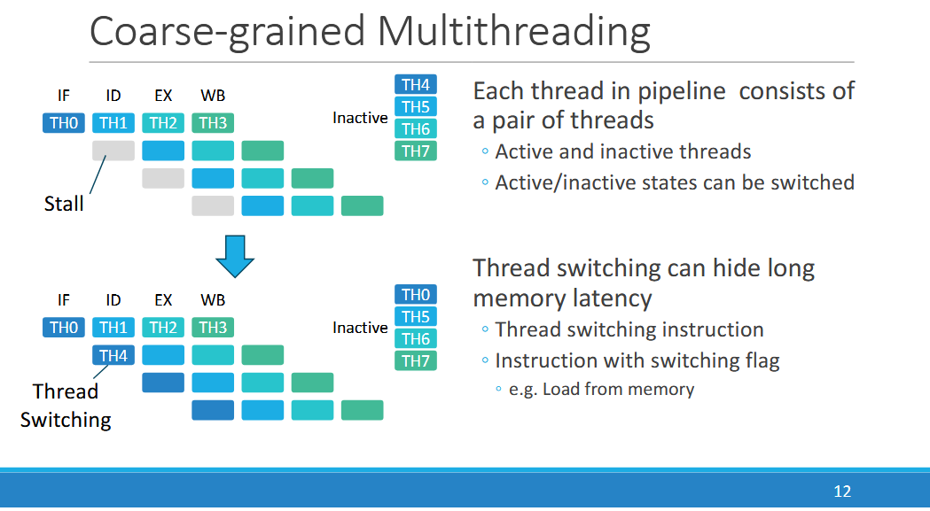
PEZY handles longer latency events by swapping active thread groups. This coarse-grained multithreading can be carried out with a thread switching instruction or a flag on a potentially long latency instruction, such as a memory load. Programmers can also opt for an automatic thread switching mode, inherited from PEZY-SC2. Depending on how well this “automatic chgthread” mode works, a PEZY PE could be treated purely as a fine-grained multithreading design. That is, thread switching and latency hiding happens automatically without help from the programmer or compiler.
GPUs issue a single instruction across a wide “wave” or “warp” of data elements, which means they lose throughput if control flow diverges within a wave. PEZY emphasizes that they’re targeting a MIMD design, with minimal branching penalties compared to a GPU. A PEZY PE feeds its four-wide FP64 unit in a SIMD fashion, and uses wider vectors for lower precision data types. The comparatively small 256-bit SIMD width makes PEZY less susceptible to branch divergence penalties than a typical GPU, which may have 1024-bit (wave32) or 2048-bit (wave64) vector lengths.
For comparison, PEZY-SC3’s PEs had a 2-wide FP64 unit. PEZY-SC4S’s wider execution units reduce instruction control costs. But the wider SIMD width could increase the chance of control flow divergence within a vector. For lower precision data types, PEZY-SC4S introduces BF16 support, in a nod to the current AI boom. However, PEZY did not spend die area or transistors on dedicated matrix multiplication units, unlike its GPU peers.
Memory Subsystem
PEZY’s memory subsystem starts with small PE-private L1 caches, with lower level caches shared between various numbers of PEs at different organizational levels. PEZY names organizational levels after administrative divisions. Groups of four PEs form a Village, four Villages form a City, 16 Cities make a Prefecture, and eight Prefectures form a chip (a State). PEZY-SC4s actually has 18 Cities in each Prefecture, or 2304 PEs in total, but two Cities in each Prefecture are disabled to provide redundancy.
A PE’s instruction cache is just 4 KB, and likely fills a role similar to the L0 instruction caches on Nvidia’s Turing. PEZY-SC3 could fetch 8B/cycle from the instruction cache and issue two instructions per cycle, implying each instruction is 4 bytes. If that’s the same in PEZY-SC4s, the 4 KB L1 instruction cache can hold 1024 instructions. That’s small compared even to a micro-op cache. A 32 KB L2 instruction cache is shared across 16 PEs, and should help handle larger instruction footprints.
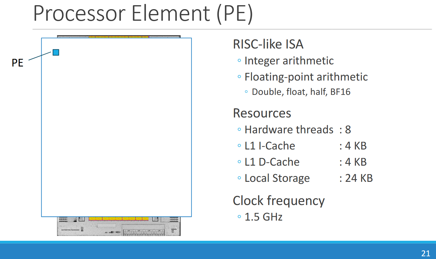
The L1 data cache is similarly small at 4 KB, though it has doubled in size compared to the 2 KB L1D in PEZY-SC3. L1D bandwidth remains unchanged at 16 bytes/cycle, which leaves PEZY-SC4s with a lower ratio of load bandwidth to compute throughput, when considering each PE’s execution units are now twice as wide. However, the massive load bandwidth available on PEZY-SC3 was likely overkill, and could only be fully utilized if a load instruction were issued every cycle. Increasing L1D capacity instead of bandwidth is likely a good tradeoff. 2 KB is really small, and 4 KB is still small. L1D load-to-use latency is 12 cycles, or three instructions because each thread only executes once every four cycles.
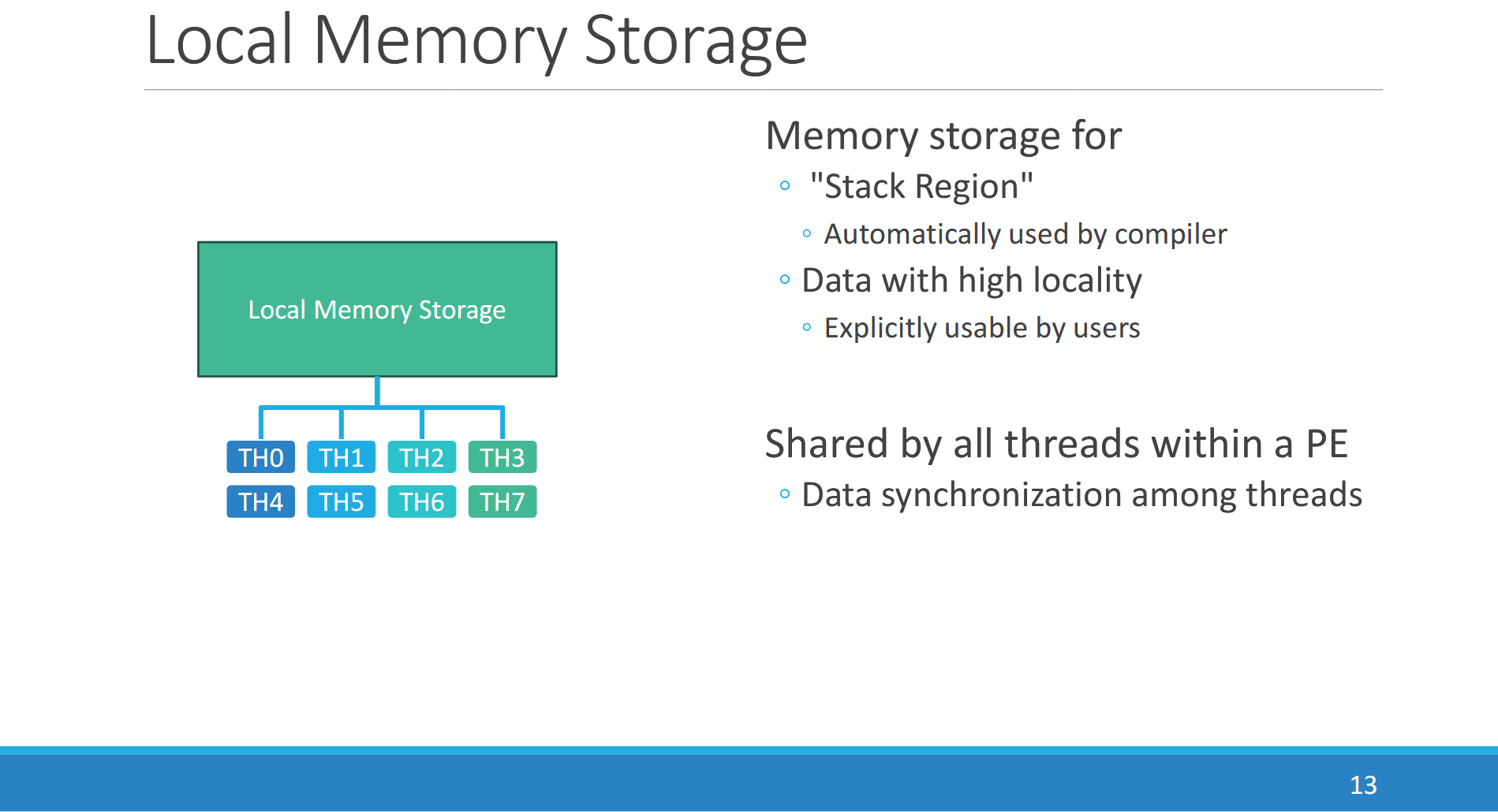
Each PE also implements local memory, much like GPUs. A 24 KB block of local storage fills a role analogous to AMD’s Local Data Share or Nvidia’s Shared Memory. It’s a directly addressed, software managed scratchpad and not a hardware managed cache. The compiler can also use a “stack region” in local storage, likely to handle register spills and function calls. Four PEs within a “village” can share local memory, possibly providing 96 KB pools of directly addressable storage. Local storage has 4 cycle load-to-use latency, so the next instruction within a thread can immediately use a previously loaded value from local storage without incurring extra delay.
A 64 KB L2 data cache is shared across 16 PEs in a “City” (four Villages), and has 20 cycle latency. There is no bandwidth reduction in going to L2D, which can also provide 16B/cycle of load bandwidth per PE. That’s 256B/cycle total per L2 instance. Matching L1D and L2D bandwidth suggests the L1D is meant to serve almost as a L0 cache, opportunistically providing lower latency while many memory loads fall through to L2D. The L2D’s low ~13-14 ns latency would match many GPU first level data caches. With a relatively low thread count per PE and small SIMD widths, PEZY likely needs low latency memory access to avoid stalls. That seems to be reflected in its L1/L2 cache setup.
System Level Organization
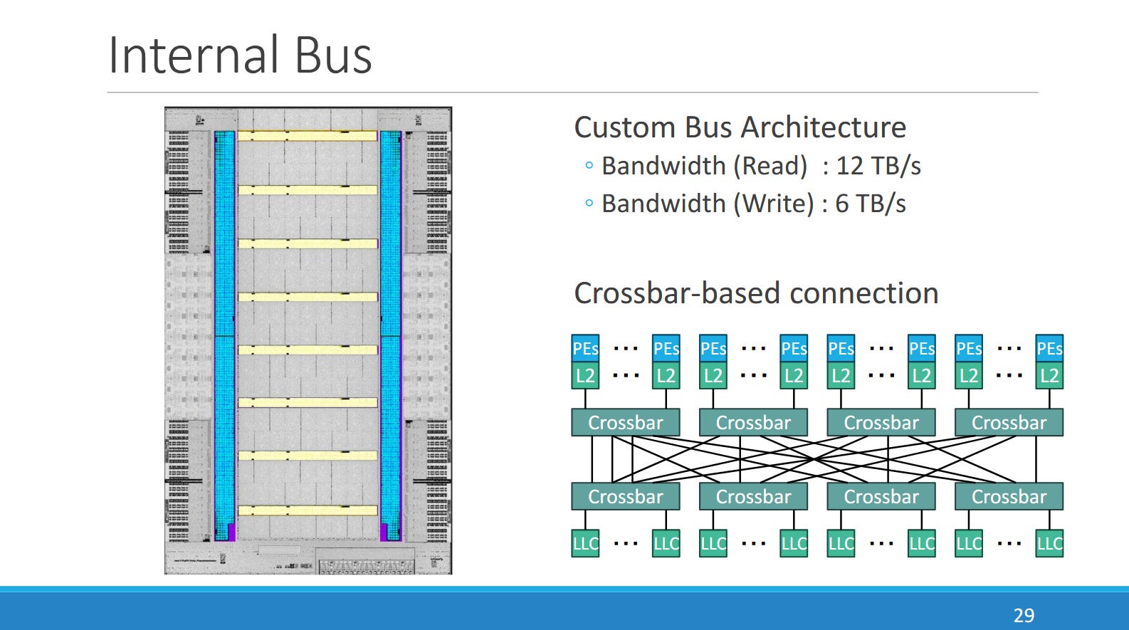
“Cities” are connected to each other and last level cache slices via crossbars, and share a 64 MB last level cache (L3). The L3 is split into slices, and can provide 12 TB/s of read bandwidth (1024 bytes/cycle) and 6 TB/s of write bandwidth (512 bytes/cycle). L3 latency is 100-160 cycles, likely depending on the distance between a PE and the L3 slice. Even the higher figure would give PEZY’s L3 better latency than AMD RDNA4’s similarly sized Infinity Cache (measured to just over 130 ns using scalar accesses). PEZY has not changed last level cache capacity compared to PEZY-SC3, keeping it at 64 MB.
Besides providing caching capacity, the last level cache handles atomic operations much like the shared L2 cache on GPUs. Similarly, PEZY uses explicit sync/flush instructions to synchronize threads and make writes visible at different levels. That frees PEZY from implementing cache coherency like a GPU, simplifying hardware.
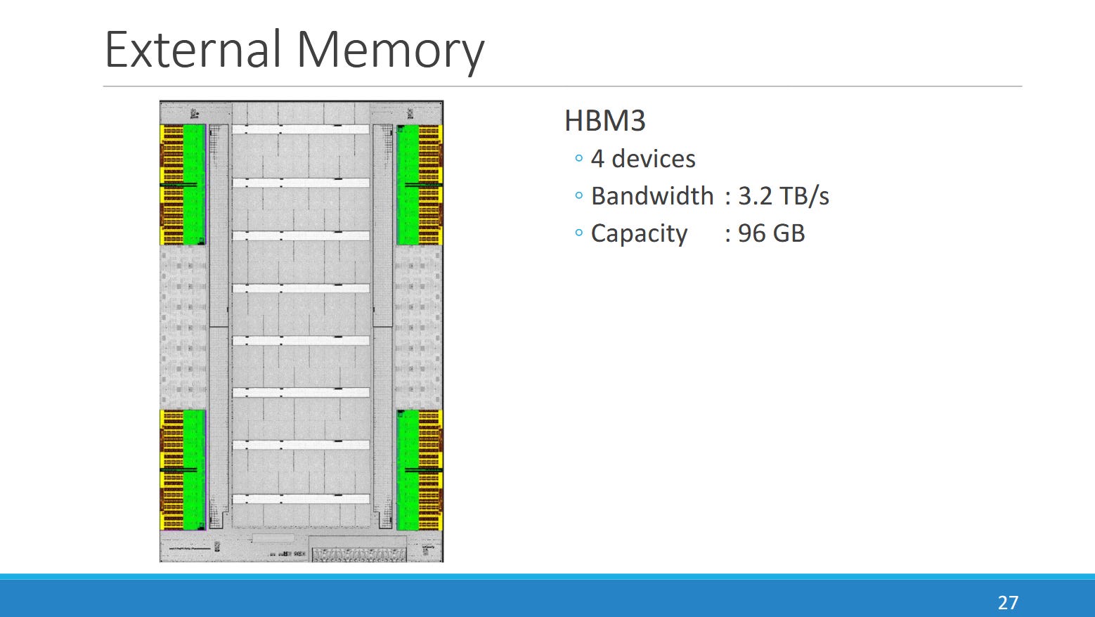
For system memory, PEZY uses four HBM3 stacks to provide 3.2 TB/s of bandwidth and 96 GB of capacity. If each HBM3 stack has a 1024-bit bus, that works out to a 8 GT/s data rate. For comparison, PEZY-SC3 had a 1.23 TB/s HBM2 setup with 32 GB of capacity, supplemented by a dual channel DDR4-3200 setup (51.2 GB/s). Likely, PEZY-SC3 used DDR4 to make up for HBM2’s capacity deficiencies. With HBM3 providing 96 GB of DRAM capacity, PEZY likely decided the DDR4 controllers were no longer needed.
Management Processor
PEZY-SC4s also includes a quad core RISC-V management processor running at 1.5 GHz. PEZY chose to use the open source Rocket Core, which is an in-order, scalar core. PEZY’s shift to RISC-V has parallels elsewhere, as many vendors seem to find the open ISA attractive. Examples include Nvidia moving towards RISC-V for their GPU management processors, replacing their prior Falcon architecture.
In PEZY-SC3, the management processor “controls the PEs and PCIe interfaces”. Likely, they help distribute work to the PEs and orchestrate transfers between the PEZY accelerator and host system memory.
Host
PEZY’s accelerators connect to the host via a standard PCIe interface. PEZY-SC4s uses a 16 lane PCIe Gen 5 interface for host communication, which is an upgrade over the PCIe Gen 4 lanes on PEZY-SC3. The host system is a standard x86-64 server, which will use an EPYC 9555P CPU (Zen 5) and Infiniband networking. One system will host four PEZY-SC4s accelerators, in a similar configuration to PEZY-SC3.
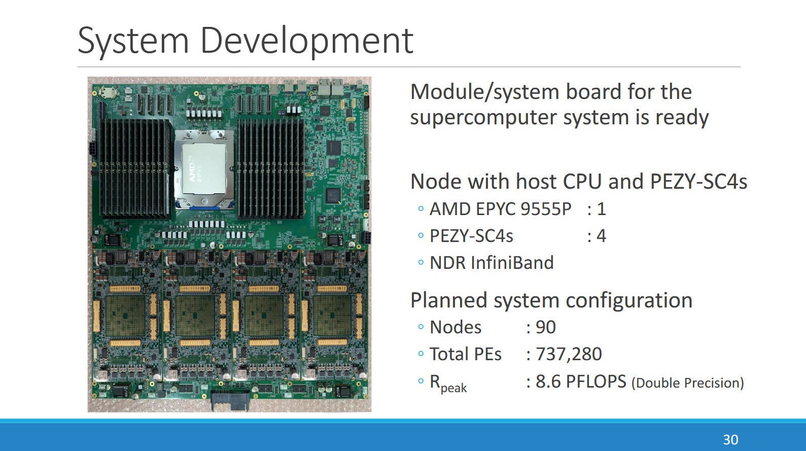
For comparison, PEZY-SC3 uses an AMD EPYC 7702P host processor, which has Zen 2 cores.
Final Words
PEZY’s aims for efficient FP64 compute while also making it easy to utilize. PEZY-SC4S has a mutli-level cache setup to balance caching capacity and speed. It uses small vectors, reducing throughput losses from branch divergence. The programming model (PZCL) is very similar to OpenCL, which should make it intuitive for anyone used to programming GPUs.
Compared to their prior PEZY-SC3S, PEZY-SC4 is more of a refinement that focuses on increased efficiency. Power draw in an earlier PEZY presentation was given at 270W, while PE-only power was estimated at 212W when running DGEMM. PEZY didn’t give any final power figures because they don’t have silicon yet. But initial figures suggest PEZY-SC4S will come in comfortably below 300W per chip.
If PEZY-SC4S can hit full throughput at 270W, it’ll achieve ~91 Gigaflops per Watt (GF/W) of FP64 performance. This is quite a bit better than Nvidia's H200, at around 49 FP64 GF/W, and somewhat less than AMD's HPC-focused MI300A, at around 110 FP64 GF/W. However there is no such thing as a free lunch. MI300A's 3D-stacked chiplet-based design was significantly more time-consuming and costly to develop along with more expensive to manufacture than PEZY's more traditional monolithic design.
Compared to the latest generation of AI-focused accelerators from AMD and NVIDIA, CDNA4 and Blackwell Ultra respectively, SC4s leads in FP64 efficiency by a considerable margin; though it is worth noting that NVIDIA have sacrificed the overwhelming majority of FP64 performance on B300 to the point where some consumer GPUs will outclass it at FP64 tasks.
The AI boom has left a bit of a blind spot for applications where high precision and result accuracy are paramount. In simulations for example, floating point error can compound over multiple iterations. Higher precision data types like FP64 can help reduce that error, and PEZY’s SC4S targets those applications.
At a higher level, efforts like PEZY-SC4s and Fujitsu’s A64FX show a curious pattern where Japan maintains domestic hardware architecture development capabilities. It’s contrasts with many other countries that still build their own supercomputers, but rely on chips designed in the US by companies like AMD, Intel, and Nvidia. From the perspective of those countries, it’s undoubtedly cheaper and less risky to rely on the US’s technological base to create the chips they need. But Japan’s approach has merits too. They can design chips tightly targeted to their needs, like energy efficient FP64 compute. It also leads to more unique designs, which I’m fascinated by. I look forward to seeing how PEZY-SC4s does once it’s deployed.
If you like the content then consider heading over to the Patreon or PayPal if you want to toss a few bucks to Chips and Cheese. Also consider joining the Discord.
References
Nvidia B200 power limit appears to be 1 kW: https://docs.nvidia.com/dgx/dgxb200-user-guide/power-capping.html
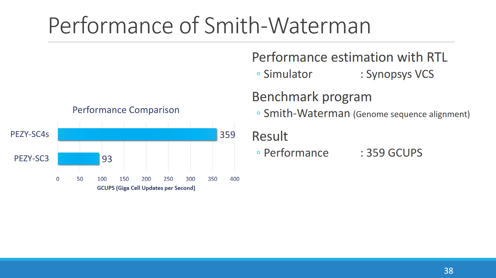
メニーコアプロセッサPEZY-SC3 によるヒトゲノム解析の高速化とPEZY-SCシリーズの展望について, presented at Supercomputing Japan 2025. Projects power consumption for PEZY-SC4S to be 270W
PEZY-SC3, 高い電力効率を実現するMIMDメニーコアプロセッサ
DGX B200 specifications: https://resources.nvidia.com/en-us-dgx-systems/dgx-b200-datasheet
https://docs.nvidia.com/cuda/blackwell-tuning-guide/index.html#increased-l2-capacity
First, thanks Chester! This is another interesting player I wasn't really aware of. Who are their current or projected customers?
And I agree, it's very interesting that Japan continues to have at least a handful of companies that keep developing very interesting processors and accelerators, the largest of which is AFAIK still Fujitsu with their upcoming Monaka CPU.
It's however also noteworthy that Rapidus's aimed-for 2 nm node wasn't mentioned. That foundry needs to fab a functional chip that can serve as proof-of-concept for their ability to fab chips.
A 12-cycle 4KB L1D at 1.5GHz seems like a mistake given that 4-cycle 64KB L1D are standard at 3+GHz... Such a tiny cache would be at worst 2 cycles, relax to 4 cycles to save power and it's still a 0-cycle load latency due to the threads.