
Panther Lake’s Reveal at ITT 2025

Hello you fine Internet folks,
At this year’s ITT, Intel announced their upcoming client SoC, Panther Lake (PTL) along with all of the improvements that they have made to this latest SoC. With a new node, improvements to the CPU cores, a brand new GPU, and more, PTL is an evolution of Intel’s prior SoC designs. So without further ado, let’s dive in.
Hope y’all enjoy!
SoC Layout
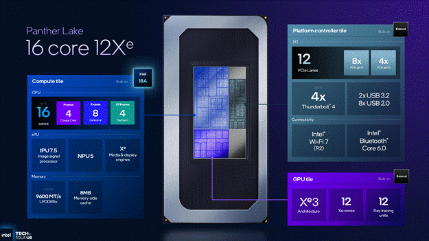
Starting with the SoC layout of Panther Lake, there are 3 active tiles on a Panther Lake CPU: Compute tile, GPU tile, and the Platform Controller tile.
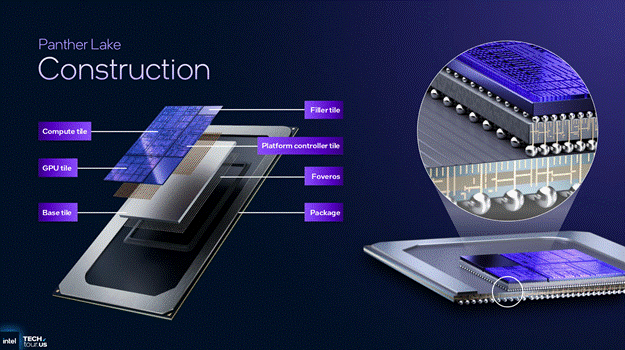
Starting with the Compute tile, the Compute tile has the main CPU complex, the Low Power CPU complex, the ISP, the NPU, the Media engines, and the 8MB Memory Side Cache alongside the 128b memory bus. The GPU tile only has the GPU compute on board and nothing else. The Platform Controller tile houses all of the I/O IP such as the PCIe, Thunderbolt, USB, etc.
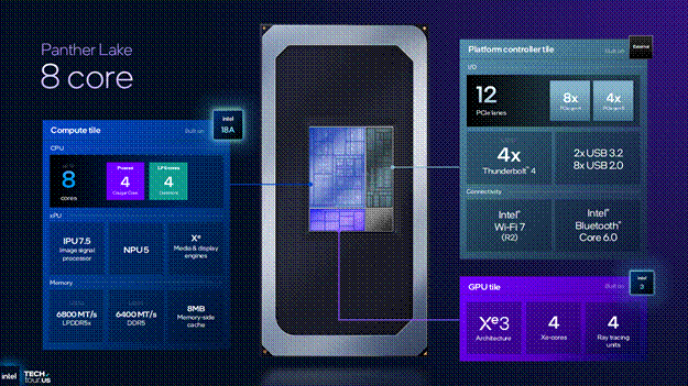
Starting with the smallest Panther Lake configuration, we have 4 P-Cores and 4 LP E-Cores paired with 8MB Memory-side Cache on the Compute Tile which is fabricated on Intel’s newest node 18A. That Compute Tile is paired with a 4 core Xe3 iGPU fabricated on Intel’s 3 process which makes this the first Intel Arc product fabricated at Intel. The Platform Controller Tile has 12 PCIe lanes split between 4 Gen 5 lanes and 8 Gen 4 lanes along with 4 Thunderbolt 4 controllers, 2 USB 3.2 & 8 USB 2.0 ports, and Wi-Fi 7 and Bluetooth 6.0.
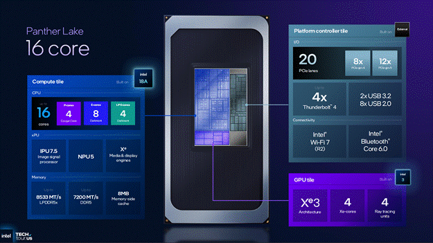
Moving to the middle configuration of Panther Lake, there has been a large change in both the Compute Tile and the Platform Controller Tile. The Compute Tile now has 4 P-Cores and 8 E-Cores which share a 18MB L3 cache with an extra 4 LP E-Cores, all of which can access the 8MB memory-side cache on board the Compute tile.
The Platform Controller tile now has an extra 8 Gen 5 PCIe lanes for a total of 20 PCIe lanes on the SoC. It was not made clear if all versions of Panther Lake use the same Platform Controller Tile fabricated on TSMC N6 or if there are 2 versions of this tile but it seems likely that all Panther Lake SoCs reuse the same physical die but with different configurations enabled.
Moving to the largest configuration of Panther Lake which keeps the same 4 P-Core, 8 E-Core, and 4 LP E-Core configuration as the middle configuration and drops the I/O configuration to the same as the smallest Panther Lake, but in exchange gains a 12 Xe3 core GPU tile which is fabricated on TSMC’s N3E process. This is the largest iGPU that Intel has made for a client SoC.
Xe3 Architecture
For many people the most exciting part of Panther Lake is going to be the brand new Xe3 architecture found in Panther Lake.
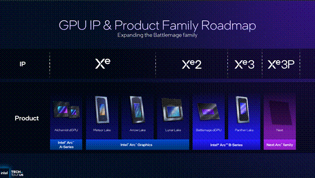
However, this new architecture will not be marketed as Intel Arc C-Series but instead will be marketed under Intel Arc B-Series just like the Battlemage series of dGPUs e.g. the B580 and B570. This is quite perplexing due to the new architecture yet the old branding which even Tom Petersen said was “confusing”.
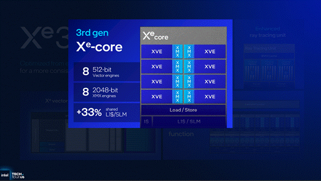
Moving on from the strange marketing decisions, one of the big changes in Xe3 is making the render slice capable of handling up to 6 Xe Cores from the 4 Xe Cores that the Xe2 render slice could support.
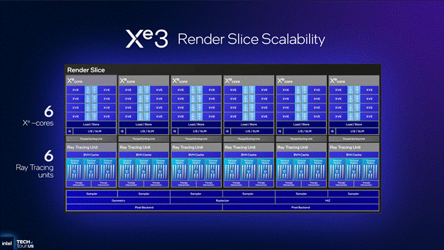
The ability of the render slice to accommodate up to 6 Xe Cores allows for the 12 Xe core configuration that is found in the largest version of Panther Lake.
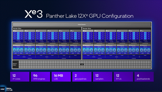
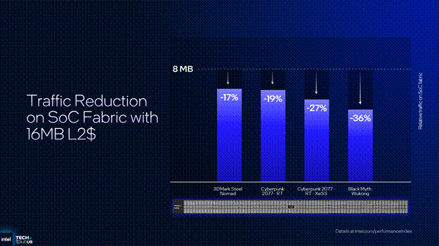
The 16MB L2 found in the 12Xe GPU reduces the traffic on the SoC fabric by up to 36% depending on the workload in question compared to a 8MB L2.
Going into the Xe Core, the amount of compute throughput that Xe3 has not changed compared to Xe2 with the same 8 512 bit Vector Engines and 8 2048 bit Matrix Engines per Xe Core but the L1/SLM capacity has increased from 192KB to 256KB.
And while Intel hasn’t increased the compute throughput of Xe3, they have made some large improvements to the frontend capabilities of Xe3. A XVE can now track up to 10 threads up from the 8 threads in Xe2’s XVE along with the single largest improvement being what Intel is calling “Variable Register Allocation”.
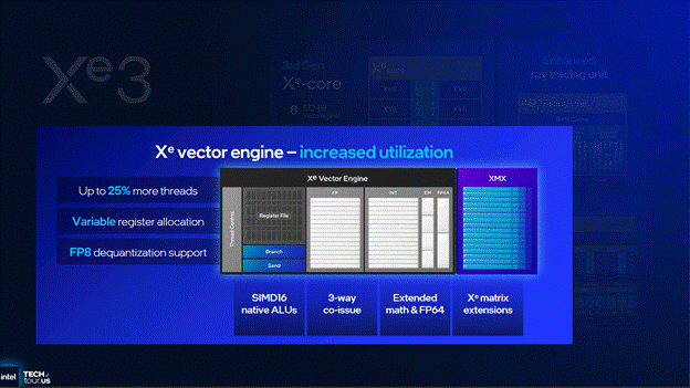
In Xe1 and prior Intel GPUs, a thread would be allocated 128 registers regardless of if that thread needed all 128 registers or not. In Xe2, Intel added the “Large GRF” mode which allows a thread to pick between 128 registers or 256 registers. Xe3 now allows a thread to allocate up to 256 registers in 32 register increments.
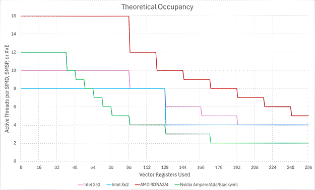
So while Xe3 kept the same 64KB per XVE register file as Xe2, the register file can now be better utilized thanks to more granularity in register allocation.
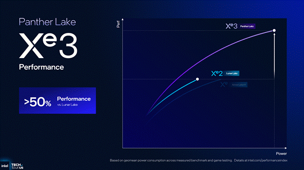
All of this, along with ray tracing units now capable of dynamic ray management, adds up to an approximate 50% performance uplift for the 12 Xe3 core iGPU in comparison to Lunar Lake’s iGPU in 3D Mark Solar Bay, Cyberpunk 2077, and Borderlands 3 albeit at higher power.
Cougar Cove and Darkmont
Going to the CPU cores found in Panther Lake, and they are much more evolution rather than revolution. If you’d like a deeper dive into the CPU cores found in Panther Cove, we did an interview with the Chief Architect of x86 Cores at Intel, Stephen Robinson, at ITT.
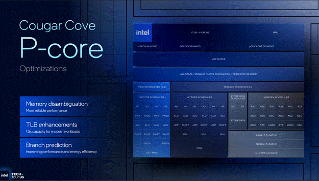
Starting with the P-Cores, codenamed Cougar Cove, Intel had increased the TLB capacity by 50% compared to Lion Cove along with improving the branch predictor by increasing some of the structure sizes in the BPU along with porting over some of the novel BPU algorithms that Intel tested in Lunar Lake.

Moving to the E-Core found in Panther Lake, codenamed Darkmont, the major improvements to Darkmont are also found in the BPU by increasing structure sizes, improving the prefetcher, and improved nanocode behavior.
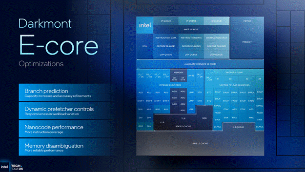
Interestingly, both Cougar Cove and Darkmont have improved the memory disambiguation (Store to Load) behavior but they each use different techniques for the improved memory disambiguation behavior. This is a case of having 2 different teams trying out different things and coming to a similar solution with different implementations.
Putting all of the microarchitecture improvements and cache improvements together and Intel is claiming a 10% single threaded improvement compared to both Arrow Lake and Lunar Lake.
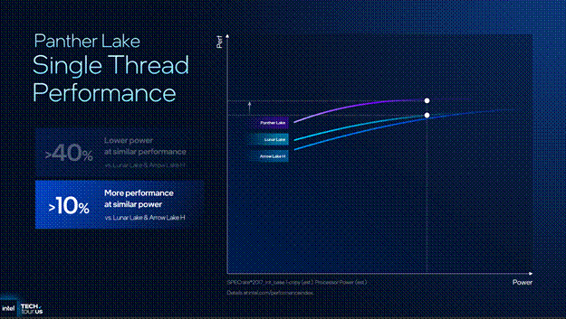
Intel is also claiming a 40% performance per watt improvement over Arrow Lake.
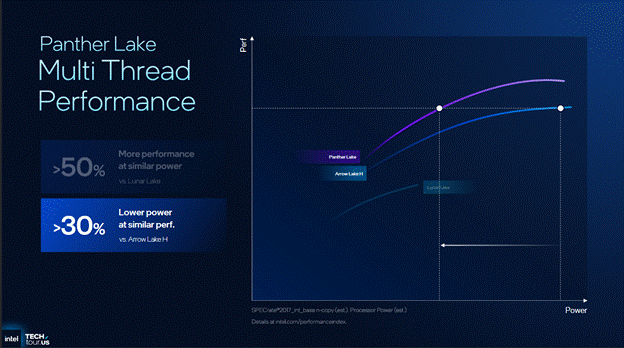
Moving to multi-thread performance, Intel is claiming a 50% performance improvement over Lunar Lake and a 30% decrease in power consumption at similar multi-thread performance.
NPU and Media Engine
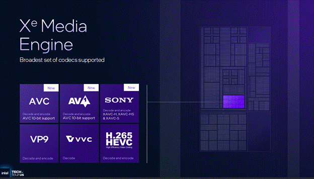
Panther Lake also comes with some improvements to other parts of the SoC such as the Media Engine now supporting AVC 10b decode and encode.
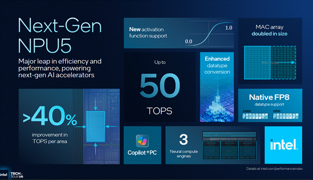
The NPU also got an upgrade with FP8 support along with shrinking the NPU by about 40% compared to the NPU found in Lunar Lake.
Final Words
Intel’s upcoming Panther Lake series of CPUs is a merging of the Lunar Lake and Arrow Lake families of SoCs in terms of the SoC design. By moving the GPU on to its own tile, Intel can now start to fabricate Arc class iGPUs on Intel’s own nodes instead of solely fabbing them on TSMC’s nodes. Perhaps this could mean that Intel could fabricate future dGPUs on Intel’s own nodes.
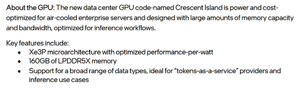
As a bit of a sidenote, Intel announced that they would be announcing an inference focused GPU at OCP 2025. Now it is unknown what node this chip is fabricated on, but now we know it is based on the Xe3P microarchitecture, has up to 160GB of LPDDR5X, and will be sampling in the second half of 2026 which hopefully means that we could be hearing more about Celestial dGPUs for consumers by the end of next year.
Moving back to Panther Lake, the official launch of Panther Lake and all of the different SKUs will occur at CES 2026 with review samples hopefully in our hands by the end of January and units on shelves shortly after. The numbers that Intel put forward for Panther Lake’s performance are promising but personally my optimism for Panther Lake has been slightly dimmed by the lackluster graphs that Intel were showing for the improvements found in Panther Lake.
Regardless, I can’t wait to test a laptop powered by a 12 Xe3 core iGPU and see what performance it can put up compared to other large iGPU client devices.
If you like the content then consider heading over to the Patreon or PayPal if you want to toss a few bucks to Chips and Cheese. Also consider joining the Discord.
Thanks George! One thing I haven't heard or read any statement from Intel about is the memory controller and improvements in latency accessing main memory. Intel's CPUs have an unfortunate tendency to have significantly worse (longer) latencies accessing DRAM than, for example, AMD's Zen CPUs.
Question 1::
4 P-Cores and 8 E-Cores which share a 18MB L3 cache with an extra 4 LP E-Cores, all of which can access the 8MB memory-side cache on board the Compute tile.
So both the 4-P-Cores, 8-E cores and 4-LPE can access the 8MB Memory Side cache ("MSC"), darkmont LPE 4 cores (which forms 1 cluster) is already expected to use 4MB of the Memory side cache (upper bound scenario) that would theoretically mean the other 4MB is left for either some of the P-Core and E-core to fight over?
Question 2::
SRAM related question, in Meteor Lake (using 155H core ultra as a discussion point) that has 24MB of L3 cache
NAME ONE-SIZE ALL-SIZE WAYS TYPE LEVEL SETS PHY-LINE COHERENCY-SIZE
L1d 49152 557056 12 Data 1 64 1 64
L1i 65536 917504 16 Instruction 1 64 1 64
L2 2097152 18874368 16 Unified 2 2048 1 64
L3 25165824 25165824 12 Unified 3 32768 1 64
155H 24MB L3 vs Panther Lake (4+8+4 SKU) which has 18MB L3 + 8 MB memory side cache.
26MB / 24MB that impiles SRAM (which is harder to scale at the foundry/process node level) increased by ~8.3% ish from Intel 4 to Intel 18A.
What is the traditional SRAM density improvements for TSMC process node jump, historically?
Is that how you would read it? (question for Geroge but Chester feel free to answer)
Question 3::
What would be your estimates for L1D$, L1I$ and L2$ size for the LPE only (Per-Core)?