
Nvidia’s B200: Keeping the CUDA Juggernaut Rolling ft. Verda (formerly DataCrunch)

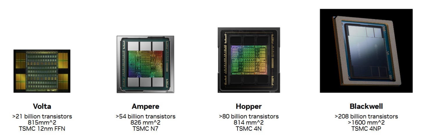
Nvidia has dominated the GPU compute scene ever since it became mainstream. The company’s Blackwell B200 GPU is the next to take up the mantle of being the go-to compute GPU. Unlike prior generations, Blackwell can’t lean heavily on process node improvements. TSMC’s 4NP process likely provides something over the 4N process used in the older Hopper generation, but it’s unlikely to offer the same degree of improvement as prior full node shrinks. Blackwell therefore moves away from Nvidia’s tried-and-tested monolithic die approach, and uses two reticle sized dies. Both dies appear to software as a single GPU, making the B200 Nvidia’s first chiplet GPU. Each B200 die physically contains 80 Streaming Multiprocessors (SMs), which are analogous to cores on a CPU. B200 enables 74 SMs per die, giving 148 SMs across the GPU. Clock speeds are similar to the H100’s high power SXM5 variant.

I’ve listed H100 SXM5 specifications in the table above, but data in the article below will be from the H100 PCIe version unless otherwise specified.
Acknowledgements
A massive thank you goes to Verda (formerly DataCrunch) for providing an instance with 8 B200s which are all connected to each other via NVLink. Verda gave us about 3 weeks with the instance to do with as we wished. We previously covered the CPU part of this VM if you want to check that part out as well.
Cache and Memory Access
B200’s cache hierarchy feels immediately familiar coming from the H100 and A100. L1 and Shared Memory are allocated out of the same SM-private pool. L1/Shared Memory capacity is unchanged from H100 and stays at 256 KB. Possible L1/Shared Memory splits have not changed either. Shared Memory is analogous to AMD’s Local Data Share (LDS) or Intel’s Shared Local Memory (SLM), and provides software managed on-chip storage local to a group of threads. Through Nvidia’s CUDA API, developers can advise on whether to prefer a larger L1 allocation, prefer equal, or prefer more Shared Memory. Those options appear to give 216, 112, and 16 KB of L1 cache capacity, respectively.
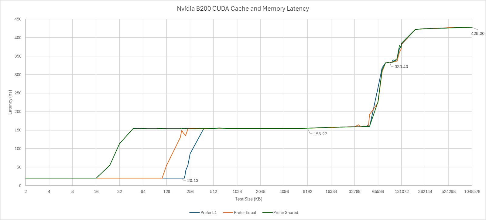
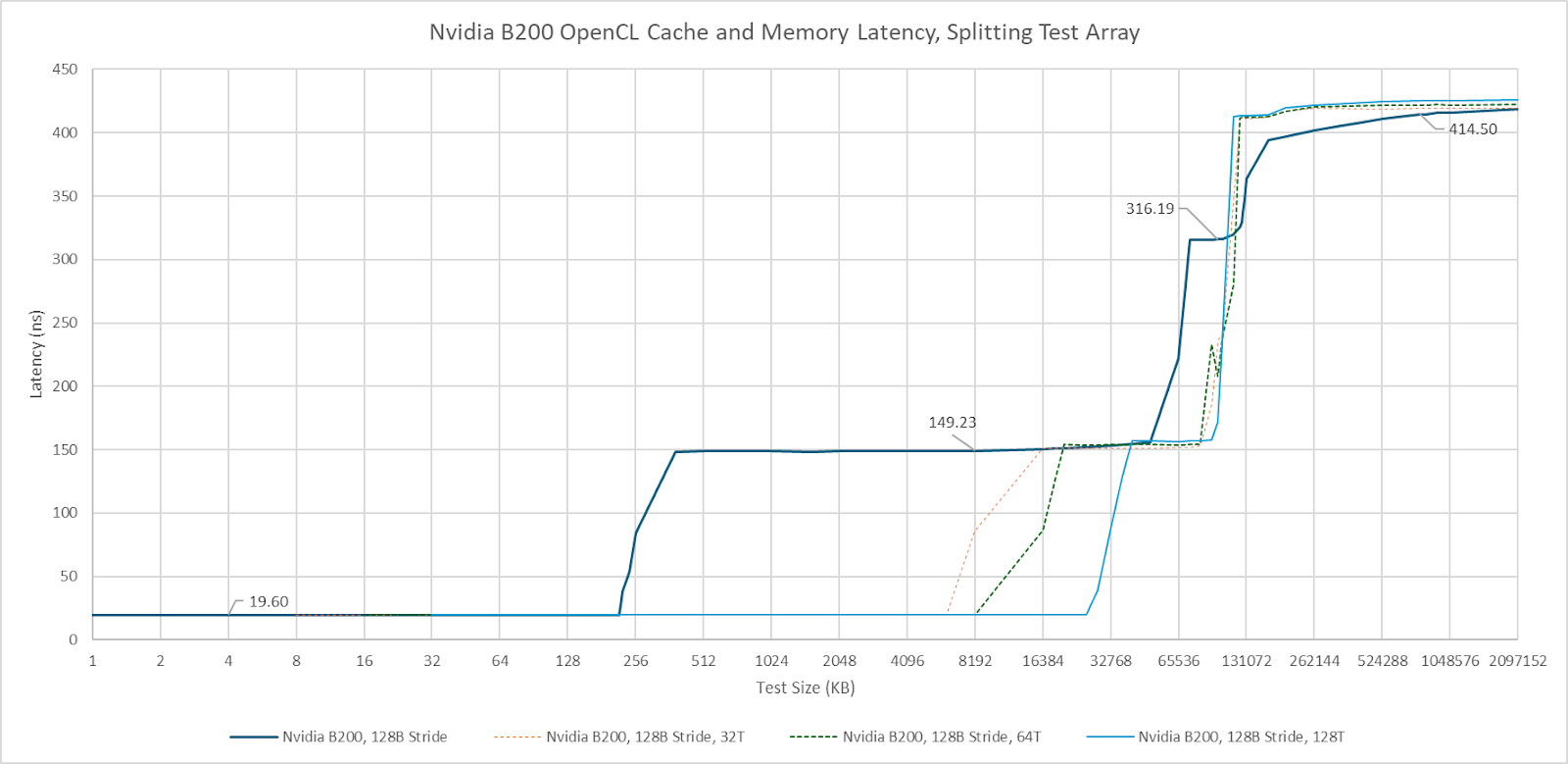
In other APIs, Shared Memory and L1 splits are completely up to Nvidia’s driver. OpenCL gets the largest 216 KB data cache allocation with a kernel that doesn’t use Shared Memory, which is quite sensible. Vulkan gets a slightly smaller 180 KB L1D allocation. L1D latency as tested with array indexing in OpenCL comes in at a brisk 19.6 ns, or 39 cycles.
As with A100 and H100, B200 uses a partitioned L2 cache. However, it’s now much larger with 126 MB of total capacity. For perspective, H100 had 50 MB of L2, and A100 had 40 MB. L2 latency to the directly attached L2 partition is similar to prior generations at about 150 ns. Latency dramatically increases as test sizes spill into the other L2 partition. B200’s cross-partition penalty is higher than its predecessors, but only slightly so. L2 partitions on B200 almost certainly correspond to its two dies. If so, the cross-die latency penalty is small, and outweighed by a single L2 partition having more capacity than H100’s entire L2.

B200 acts like it has a triple level cache setup from a single thread’s perspective. The L2’s partitioned nature can be shown by segmenting the pointer chasing array and having different threads traverse each segment. Curiously, I need a large number of threads before I can access most of the 126 MB capacity without incurring cross-partition penalties. Perhaps Nvidia’s scheduler tries to fill one partition’s SMs before going to the other.
AMD’s Radeon Instinct MI300X has a true triple-level cache setup, which trades blows with B200’s. Nvidia has larger and faster L1 caches. AMD’s L2 trades capacity for a latency advantage compared to Nvidia. Finally, AMD’s 256 MB last level cache offers an impressive combination of latency and high capacity. Latency is lower than Nvidia’s “far” L2 partition.
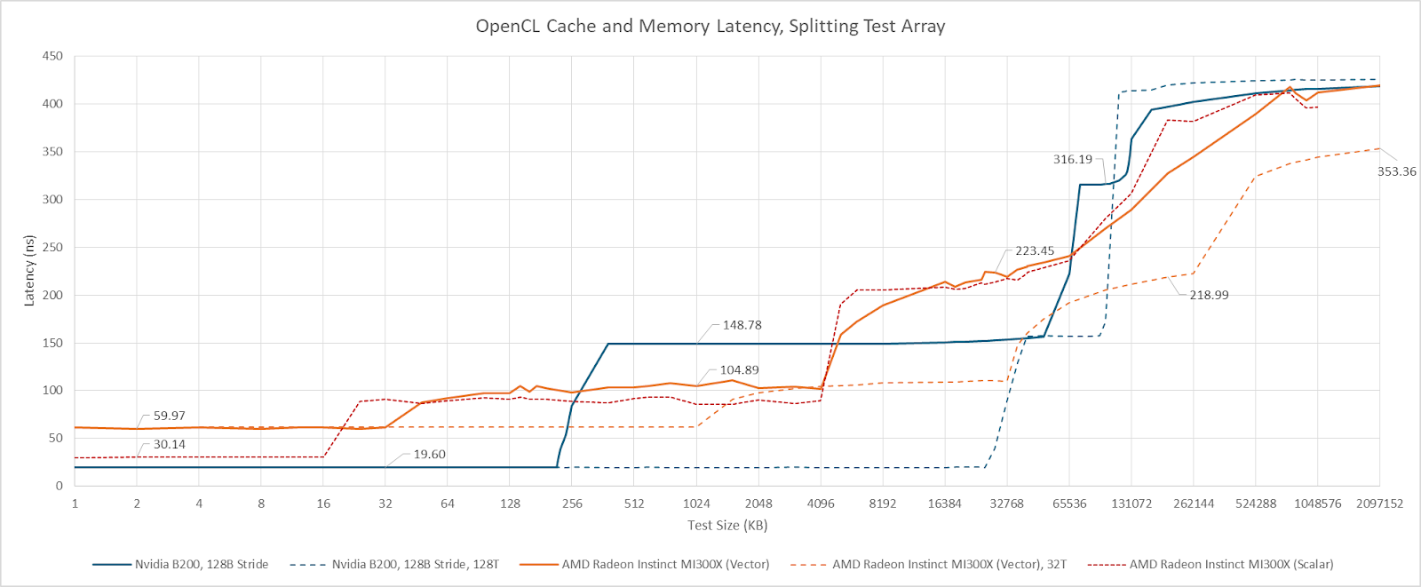
One curiosity is that both the MI300X and B200 show more uniform latency across the last level cache when I run multiple threads hitting a segmented pointer chasing array. However, the reasons behind that latency increase are different. The latency increase past 64 MB on AMD appears to be caused by TLB misses, because testing with a 4 KB stride shows a latency increase at the same point. Launching more threads brings more TLB instances into play, mitigating address translation penalties. Cutting out TLB miss penalties also lowers measured VRAM latency on the MI300X. On B200, splitting the array didn’t lower measured VRAM latency, suggesting TLB misses either weren’t a significant factor with a single thread, or bringing on more threads didn’t reduce TLB misses. B200 thus appears to have higher VRAM latency than the MI300X, as well as the older H100 and A100. Just as with the L2 cross-partition penalty, the modest nature of the latency regression versus H100/A100 suggests Nvidia’s multi-die design is working well.

OpenCL’s local memory space is backed by Nvidia’s Shared Memory, AMD’s LDS, or Intel’s SLM. Testing local memory latency with array accesses shows B200 continuing the tradition of offering excellent Shared Memory latency. Accesses are faster than on any AMD GPU I’ve tested so far, including high-clocked members of the RDNA line. AMD’s CDNA-based GPUs have much higher local memory latency.

Atomic operations on local memory can be used to exchange data between threads in the same workgroup. On Nvidia, that means threads running on the same SM. Bouncing data between threads using atomic_cmpxchg shows latency on par with AMD’s MI300X. As with pointer chasing latency, B200 gives small incremental improvements over prior generations. AMD’s RDNA line does very well in this test compared to big compute GPUs.
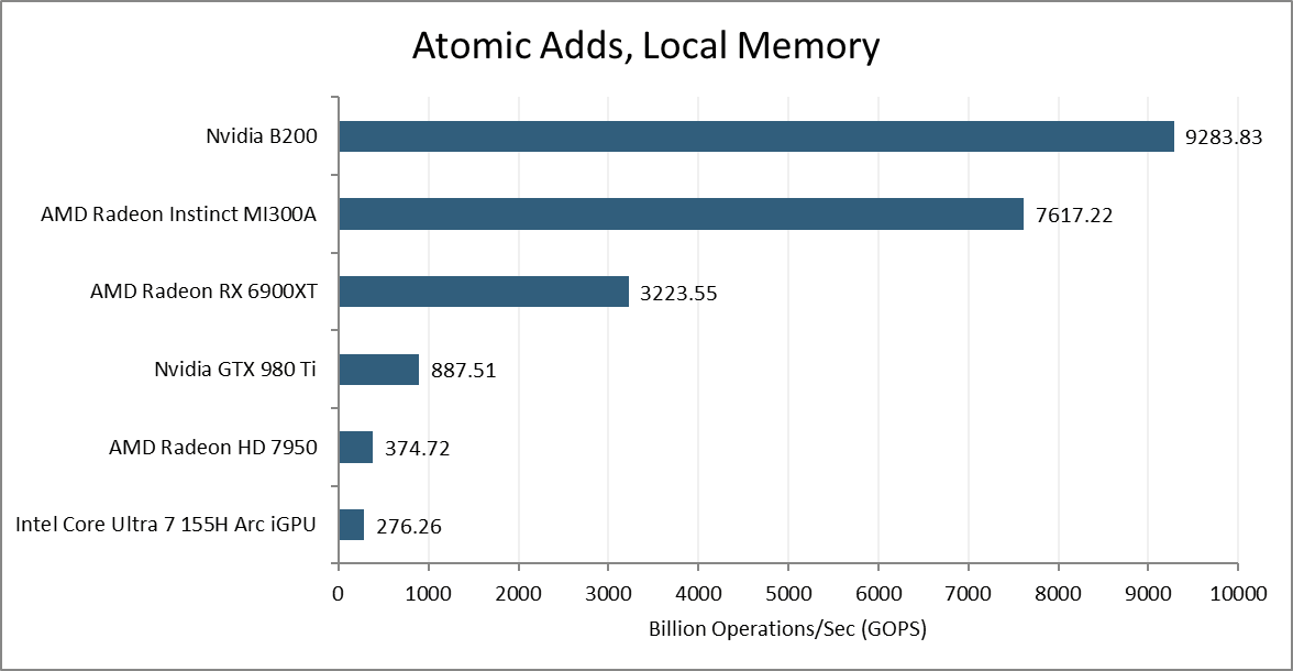
Modern GPUs use dedicated atomic ALUs to handle operations like atomic adds and increments. Testing with atomic_add gives a throughput of 32 operations per cycle, per SM on the B200. I wrote this test after MI300X testing was concluded, so I only have data from the MI300A. Like GCN, AMD’s CDNA3 Compute Units can sustain 16 atomic adds per cycle. That lets the B200 pull ahead despite having a lower core count.
Bandwidth Measurements
A higher SM count gives B200 a large L1 cache bandwidth advantage over its predecessors. It also catches up to AMD’s MI300X from OpenCL testing. Older, smaller consumer GPUs like the RX 6900XT are left in the dust.

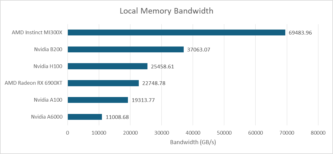
Local memory offers the same bandwidth as L1 cache hits on the B200, because both are backed by the same block of storage. That leaves AMD’s MI300X with a large bandwidth lead. Local memory is more difficult to take advantage of because developers must explicitly manage data movement, while a cache automatically takes advantage of locality. But it is an area where the huge MI300X continues to hold a lead.
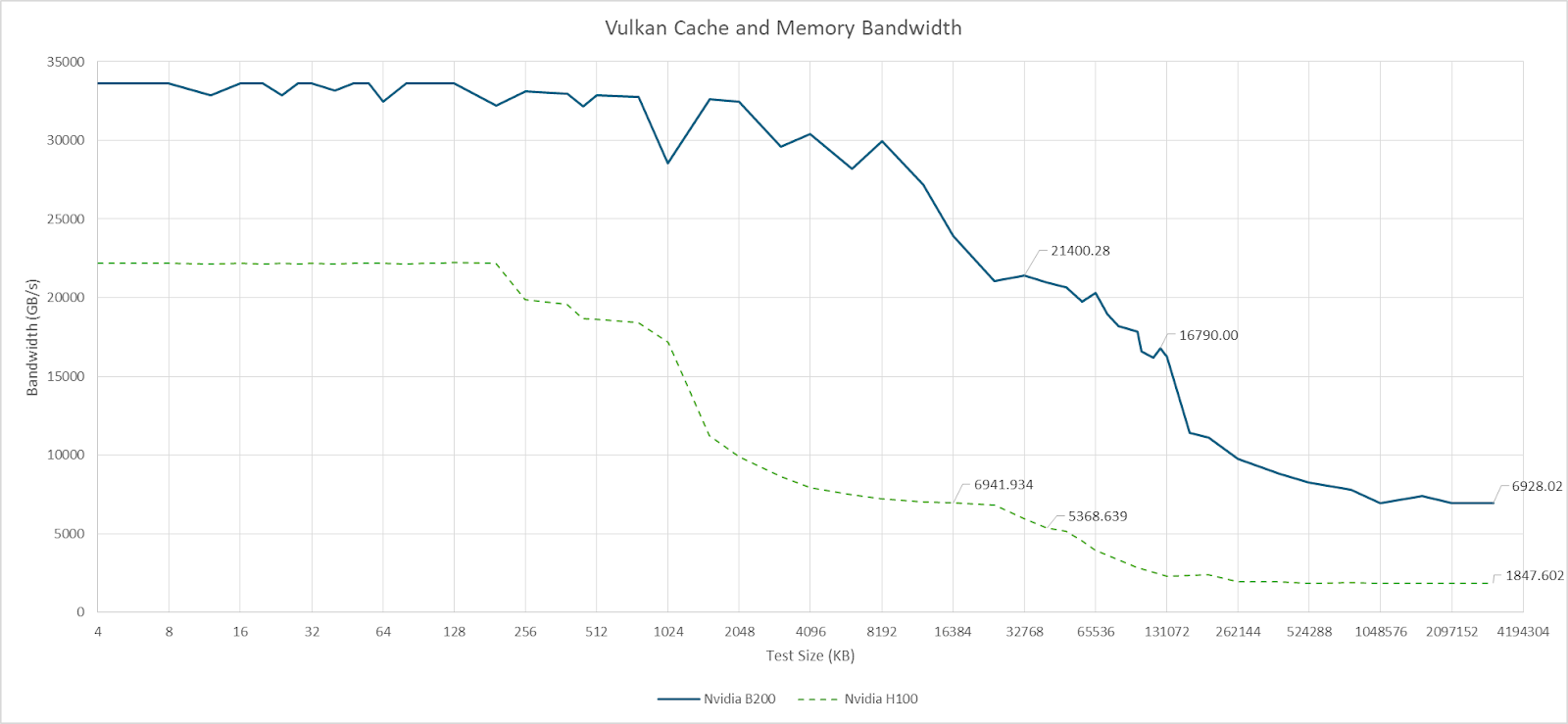
Nemez’s Vulkan-based benchmark provides an idea of what L2 bandwidth is like on the B200. Smaller data footprints contained within the local L2 partition achieve 21 TB/s of bandwidth. That drops to 16.8 TB/s when data starts crossing between the two partitions. AMD’s MI300X has no graphics API support and can’t run Vulkan compute. However, AMD has specified that the 256 MB Infinity Cache provides 14.7 TB/s of bandwidth. The MI300X doesn’t need the same degree of bandwidth from Infinity Cache because the 4 MB L2 instances in front of it should absorb a good chunk of L1 miss traffic.
The B200 offers a large bandwidth advantage over the outgoing H100 at all levels of the cache hierarchy. Thanks to HBM3E, B200 also gains a VRAM bandwidth lead over the MI300X. While the MI300X also has eight HBM stacks, it uses older HBM3 and tops out at 5.3 TB/s.
Global Memory Atomics
AMD’s MI300X showed varying latency when using atomic_cmpxchg to bounce values between threads. Its complex multi-die setup likely contributed to this. The same applies to B200. Here, I’m launching as many single-thread workgroups as GPU cores (SMs or CUs), and selecting different thread pairs to test. I’m using an access pattern similar to that of a CPU-side core to core latency test, but there’s no way to influence where each thread gets placed. Therefore, this isn’t a proper core to core latency test and results are not consistent between runs. But it is enough to display latency variation, and show that the B200 has a bimodal latency distribution.
Latency is 90-100 ns in good cases, likely when threads are on the same L2 partition. Bad cases land in the 190-220 ns range, and likely represents cases when communication crosses L2 partition boundaries. Results on AMD’s MI300X range from ~116 to ~202 ns. B200’s good case is slightly better than AMD’s, while the bad case is slightly worse.

Thread to thread latency is generally higher on datacenter GPUs compared to high clocked consumer GPUs like the RX 6900XT. Exchanging data across a GPU with hundreds of SMs or CUs is challenging, even in the best cases.
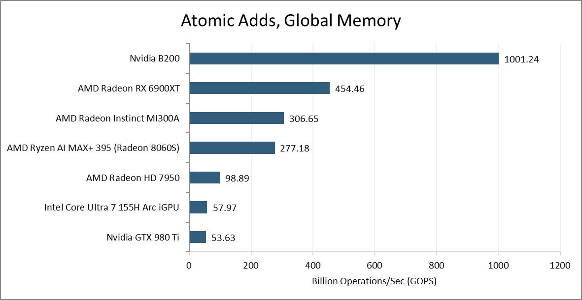
Atomic adds on global memory are usually handled by dedicated ALUs at a GPU-wide shared cache level. Nvidia’s B200 can sustain just short of 512 such operations per cycle across the GPU. AMD’s MI300A does poorly in this test, achieving lower throughput than the consumer oriented RX 6900XT.
Compute Throughput
Increased SM count gives the B200 higher compute throughput than the H100 across most vector operations. However, FP16 is an exception. Nvidia’s older GPUs could do FP16 operations at twice the FP32 rate. B200 cannot.
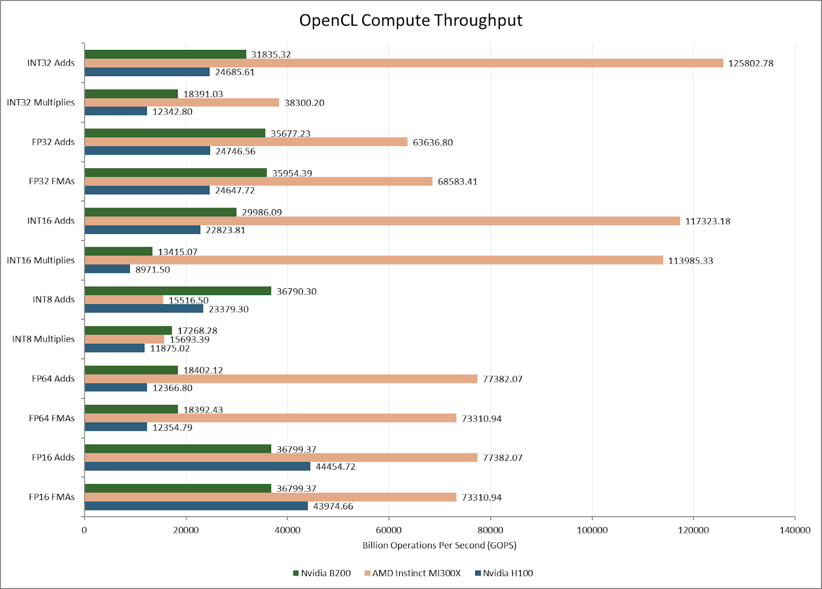
AMD’s MI300X can also do double rate FP16 compute. Likely, Nvidia decided to focus on handling FP16 with the Tensor Cores, or matrix multiplication units. Stepping back, the MI300X’s massive scale blows out both the H100 and B200 for most vector operations. Despite using older process nodes, AMD’s aggressive chiplet setup still holds advantages.
Tensor Memory
B200 targets AI applications, and no discussion would be complete without covering its machine learning optimizations. Nvidia has used Tensor Cores, or dedicated matrix multiplication units, since the Turing/Volta generation years ago. GPUs expose a SIMT programming model where developers can treat each lane as an independent thread, at least from a correctness perspective. Tensor Cores break the SIMT abstraction by requiring a certain matrix layout across a wave, or vector. Blackwell’s 5th generation Tensor Cores go one step further, and have a matrix span multiple waves in a workgroup (CTA).
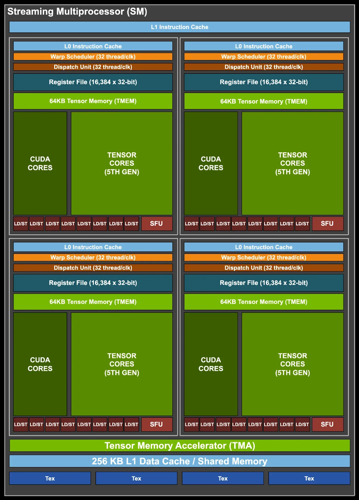
Blackwell also introduces Tensor Memory, or TMEM. TMEM acts like a register file dedicated to the Tensor Cores. Developers can store matrix data in TMEM, and Blackwell’s workgroup level matrix multiplication instructions use TMEM rather than the register file. TMEM is organized as 512 columns by 128 rows with 32-bit cells. Each wave can only access 32 TMEM rows, determined by its wave index. That implies each SM sub-partition has a 512 column by 32 row TMEM partition. A “TensorCore Collector Buffer” can take advantage of matrix data reuse, taking the role of a register reuse cache for TMEM.
TMEM therefore works like the accumulator register file (Acc VGPRs) on AMD’s CDNA architecture. CDNA’s MFMA matrix instructions similarly operate on data in the Acc VGPRs, though MFMA can also take source matrices from regular VGPRs. On Blackwell, only the older wave-level matrix multiplication instructions take regular register inputs. Both TMEM and CDNA’s Acc VGPRs have 64 KB of capacity, giving both architectures a 64+64 KB split register file per execution unit partition. The regular vector execution units cannot take inputs from TMEM on Nvidia, or the Acc VGPRs on AMD.
While Blackwell’s TMEM and CDNA’s Acc VGPRs have similar high level goals, TMEM is a more capable and mature implementation of the split register file idea. CDNA had to allocate the same number of Acc and regular VGPRs for each wave. Doing so likely simplified bookkeeping, but creates an inflexible arrangement where mixing matrix and non-matrix waves would make inefficient use of register file capacity. TMEM in contrast uses a dynamic allocation scheme similar in principle to dynamic VGPR allocation on AMD’s RDNA4. Each wave starts with no TMEM allocated, and can allocate 32 to 512 columns in powers of two. All rows are allocated at the same time, and waves must explicitly release allocated TMEM before exiting. TMEM can also be loaded from Shared Memory or the regular register file, while CDNA’s Acc VGPRs can only be loaded through regular VGPRs. Finally, TMEM can optionally “decompress” 4 or 6-bit data types to 8 bits as data is loaded in.
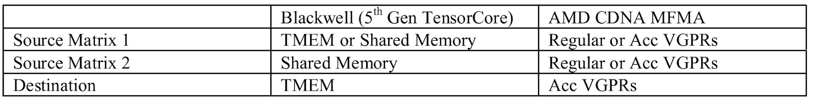
Compared to prior Nvidia generations, adding TMEM helps reduce capacity and bandwidth pressure on the regular register file. Introducing TMEM is likely easier than expanding the regular register file. Blackwell’s CTA-level matrix instructions can sustain 1024 16-bit MAC operations per cycle, per partition. Because one matrix input always comes from Shared Memory, TMEM only has to read one row and accumulate into another row every cycle. The regular vector registers would have to sustain three reads and one write per cycle for FMA instructions. Finally, TMEM doesn’t have to be wired to the vector units. All of that lets Blackwell act like it has a larger register file for AI applications, while allowing hardware simplifications. Nvidia has used 64 KB register files since the Kepler architecture from 2012, so a register file capacity increase feels overdue. TMEM delivers that in a way.
On AMD’s side, CDNA2 abandoned dedicated Acc VGPRs and merged all of the VGPRs into a unified 128 KB pool. Going for a larger unified pool of registers can benefit a wider range of applications, at the cost of not allowing certain hardware simplifications.
Some Light Benchmarking
Datacenter GPUs traditionally have strong FP64 performance, and that continues to be the case for B200. Basic FP64 operations execute at half the FP32 rate, making it much faster than consumer GPUs. In a self penned benchmark, B200 continues to do well compared to both consumer GPUs and H100. However, the MI300X’s massive size shows through even though it’s an outgoing GPU.
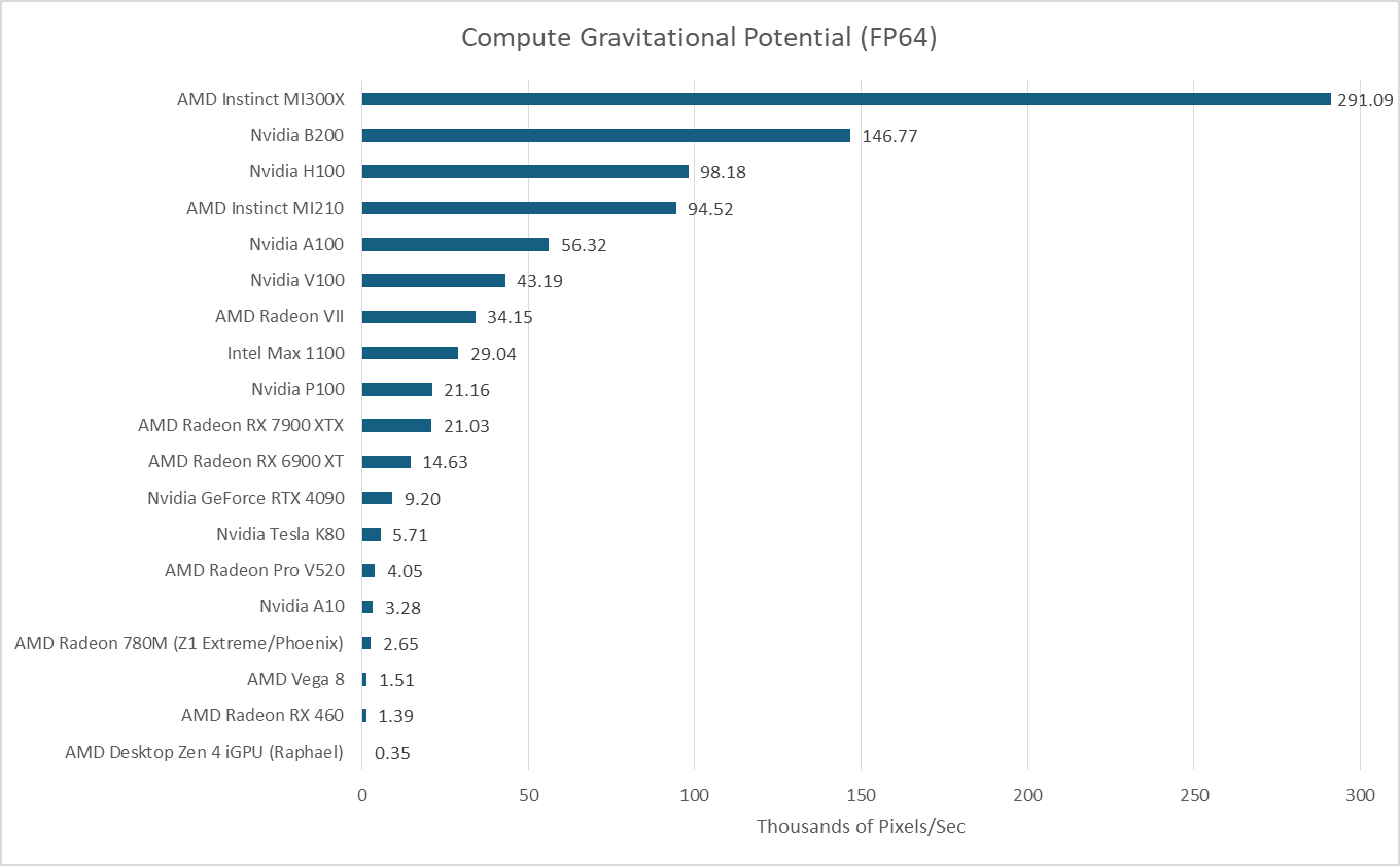
In the workload above, I take a 2360x2250 FITS file with column density values and output gravitational potential values with the same dimensions. The data footprint is therefore 85 MB. Even without performance counter data, it’s safe to assume it fits in the last level cache on both MI300X and B200.
FluidX3D is a different matter. Its benchmark uses a 256x256x256 cell configuration and 93 bytes per cell in FP32 mode, for a 1.5 GB memory footprint. Its access patterns aren’t cache friendly, based on testing with performance counters on Strix Halo. FluidX3D plays well into B200’s VRAM bandwidth advantage, and the B200 now pulls ahead of the MI300X.
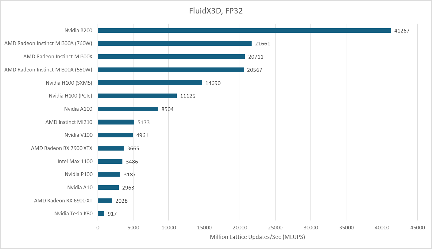
FluidX3D can also use 16-bit floating point formats for storage, reducing memory capacity and bandwidth requirements. Computations still use FP32 and format conversion costs extra compute, so the FP16 formats result in a higher compute to bandwidth ratio. That typically improves performance because FluidX3D is so bandwidth bound. When using IEEE FP16 for storage, AMD’s MI300A catches up slightly but leaves the B200 ahead by a large margin.

Another FP16C format reduces the accuracy penalty associated with using 16 bit storage formats. It’s a custom floating point format without hardware support, which further drives up the compute to bandwidth ratio.
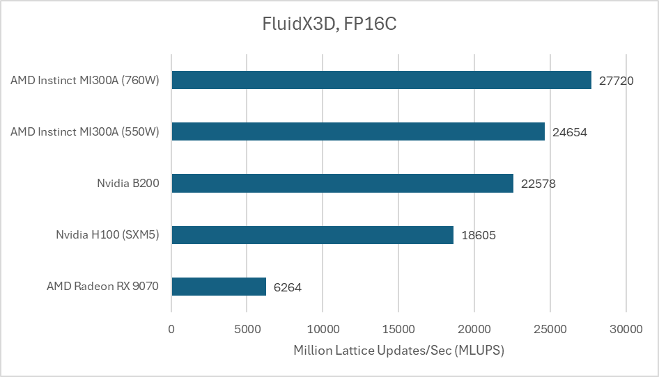
With compute front and center again, AMD’s MI300A pulls ahead. The B200 doesn’t do badly, but it can’t compete with the massive compute throughput that AMD’s huge chiplet GPU provides.
Teething Issues
We encountered three GPU hangs over several weeks of testing. The issue manifested with a GPU process getting stuck. Then, any process trying to use any of the system’s eight GPUs would also hang. None of the hung processes could be terminated, even with SIGKILL. Attaching GDB to one of them would cause GDB to freeze as well. The system remained responsive for CPU-only applications, but only a reboot restored GPU functionality. nvidia-smi would also get stuck. Kernel messages indicated the Nvidia unified memory kernel module, or nvidia_uvm, took a lock with preemption disabled.
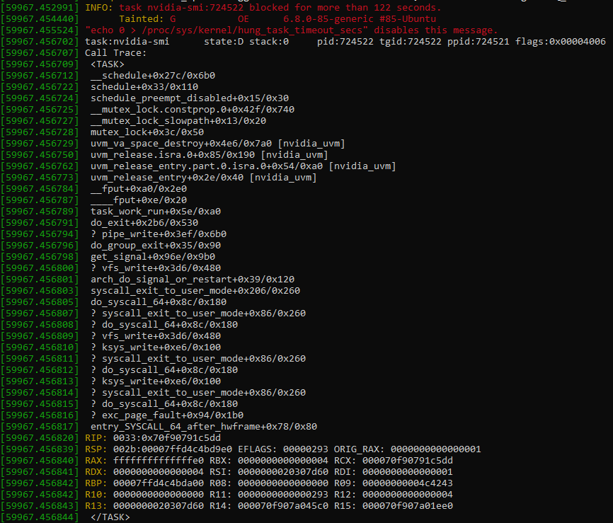
The stack trace suggests Nvidia might be trying to free allocated virtual memory, possibly on the GPU. Taking a lock makes sense because Nvidia probably doesn’t want other threads accessing a page freelist while it’s being modified. Why it never leaves the critical section is anyone’s guess. Perhaps it makes a request to the GPU and never gets a response. Or perhaps it’s purely a software deadlock bug on the host side.
# nvidia-smi -r
The following GPUs could not be reset:
GPU 00000000:03:00.0: In use by another client
GPU 00000000:04:00.0: In use by another client
GPU 00000000:05:00.0: In use by another client
GPU 00000000:06:00.0: In use by another client
GPU 00000000:07:00.0: In use by another client
GPU 00000000:08:00.0: In use by another client
GPU 00000000:09:00.0: In use by another client
GPU 00000000:0A:00.0: In use by another client
Hangs like this aren’t surprising. Hardware acceleration adds complexity, which translates to more failure points. But modern hardware stacks have evolved to handle GPU issues without a reboot. Windows’s Timeout Detection and Recovery (TDR) mechanism for example can ask the driver to reset a hung GPU. nvidia-smi does offer a reset option. But frustratingly, it doesn’t work if the GPUs are in use. That defeats the purpose of offering a reset option. I expect Nvidia to iron out these issues over time, especially if the root cause lies purely with software or firmware. But hitting this issue several times within such a short timespan isn’t a good sign, and it would be good if Nvidia could offer ways to recover from such issues without a system reboot.
Final Words
Nvidia has made the chiplet jump without any major performance concessions. B200 is a straightforward successor to H100 and A100, and software doesn’t have to care about the multi-die setup. Nvidia’s multi-die strategy is conservative next to the 12-die monster that is AMD’s MI300X. MI300X retains some surprising advantages over Nvidia’s latest GPU, despite being an outgoing product. AMD’s incoming datacenter GPUs will likely retain those advantages, while catching up in areas that the B200 has pulled ahead in. The MI350X for example will bring VRAM bandwidth to 8 TB/s.
But Nvidia’s conservative approach is understandable. Their strength doesn’t lie in being able to build the biggest, baddest GPU around the block. Rather, Nvidia benefits from their CUDA software ecosystem. GPU compute code is typically written for Nvidia GPUs first. Non-Nvidia GPUs are an afterthought, if they’re thought about at all. Hardware isn’t useful without software to run on it, and quick ports won’t benefit from the same degree of optimization. Nvidia doesn’t need to match the MI300X or its successors in every area. They just have to be good enough to prevent people from filling in the metaphorical CUDA moat. Trying to build a monster to match the MI300X is risky, and Nvidia has every reason to avoid risk when they have a dominant market position.

Still, Nvidia’s strategy leaves AMD with an opportunity. AMD has everything to gain from being ambitious and taking risks. GPUs like the MI300X are impressive showcases of hardware engineering, and demonstrate AMD’s ability to take on ambitious design goals. It’ll be interesting to see whether Nvidia’s conservative hardware strategy and software strength will result in its continued dominance.
Again, a massive thank you goes to Verda (formerly DataCrunch) without which this article would not be possible! If you want to try out the B200 or test other NVIDIA GPUs yourself, Verda is offering free trial credits specifically for Chips & Cheese readers. Simply enter the code “CHEESE-B200” and redeem 50$ worth of credit and follow these instructions on how to redeem coupon credits.
If you like the content then consider heading over to the Patreon or PayPal if you want to toss a few bucks to Chips and Cheese. Also consider joining the Discord.
"Nvidia’s conservative hardware" This is a f***ing 1600mm² die, it's not conservative. lol
Thanks for the impressive testing, as always. I have an article idea/request that seems like it would be well within your expertise - looking at the new CUDA tile programming model and how it may or may not bring other API’s closer to native CUDA performance on NVIDIA’s GPUs.