Nintendo Switch’s iGPU: Maxwell Nerfed Edition
Graphics performance is vital for any console chip. Nintendo selected Nvidia’s Tegra X1 for their Switch handheld console. Tegra X1 is designed to maximize graphics performance in a limited power envelope, making it a natural choice for a console. And naturally for a Nvidia designed SoC, the Tegra X1 leverages the company’s Maxwell graphics architecture.
Maxwell is better known for serving in Nvidia’s GTX 900 series discrete GPUs. There, it provided excellent performance and power efficiency. But Maxwell was primarily designed to serve in discrete GPUs with substantial area and power budgets. To fit Tegra X1’s low power requirements, Maxwell had to adapt to fit into a smaller power envelope.
Today, we’ll be running a few microbenchmarks on Nvidia’s Tegra X1, as implemented in the Nintendo Switch. We’re using Nemes’s Vulkan microbenchmark because the Tegra X1 does not support OpenCL. I also couldn’t get CUDA working on the platform.
Overview
Tegra X1 implements two Maxwell Streaming Multiprocessors, or SMs. SMs are basic building blocks in Nvidia’s GPUs and roughly analogous to CPU cores. As a Maxwell derivative, the Tegra X1’s SMs feature a familiar four scheduler partitions each capable of executing a 32-wide vector (warp) per cycle.
Tegra X1’s Maxwell is a bit different from the typical desktop variant. Shared memory, which is a fast software managed scratchpad, sees its capacity cut from 96 KB to 64 KB. Lower end Maxwell parts like the GM107 used in the GTX 750 Ti also have 64 KB of Shared Memory in their SMs, so there’s a chance Tegra could be using the GM107 Maxwell flavor. But L1 cache size is cut in half too, from 24 KB to 12 KB per two SM sub partitions (SMSPs). I don’t know if GM107 uses the smaller cache size. But even if it does, Tegra Maxwell sets itself apart with packed FP16 execution4, which can double floating point throughput (subject to terms and conditions).
Besides having less fast storage in each SM, Nintendo has chosen to run the iGPU at a low 768 MHz. For comparison, the EVGA GTX 980 Ti also tested here boosts at up to 1328 MHz, and typically runs above 1200 MHz. This high clock speed is shared with GM107, which averages around 1140 MHz.
Tegra X1’s low iGPU clock could be unique to the Nintendo Switch. Nvidia’s datasheet states the GPU should be capable of 1024 FP16 GFLOPs at reasonable temperatures. Working backwards, 1024 FP16 GFLOPS would be achieved with each of the iGPU’s 256 lanes working on two packed operands and performing two operations (a fused multiply add) on them at 1 GHz. However, I don’t have access to any other Tegra X1 platforms. Therefore, the rest of this article will evaluate Tegra X1 as implemented in the Switch, including the low clocks set by Nintendo.
Cache and Memory Latency
Tegra X1’s iGPU sees high latency throughout its memory hierarchy due to low clocks. If we focus on clock cycle counts, both the GTX 980 Ti and Tegra’s iGPU have about 110 cycles of L1 cache latency. Even though Tegra X1 has a smaller L1 cache running at lower clocks, Nvidia was unable to make the pipeline shorter. L2 cache latency is approximately 166 cycles on Tegra X1 compared to the GTX 980 Ti’s 257 cycles. Tegra taking fewer cycles to access its 256 KB L2 makes sense because the intra-GPU interconnect is smaller. But it’s not really a victory because the desktop part’s higher clock speed puts it ahead in absolute terms. Finally, VRAM latency is very high at over 400 ns.
Intel’s Gen 9 (Skylake) integrated graphics provides an interesting comparison. Skylake’s GT2 graphics are found across a wide range of parts, and the HD 630 variant in later Skylake-derived generations is similar. While not designed primarily for gaming, it can be pressed into service by gamers without a lot of disposable income.
Intel has an interesting scheme for GPU caching. Global memory accesses from compute kernels go straight to an iGPU wide cache, which Intel calls a L3. To reduce confusion, I’ll use “L3” to refer to the iGPU’s private cache, and LLC to refer to the i5-6600K’s 6 MB of cache shared by the CPU and iGPU. The HD 530’s L3 has 768 KB of physical capacity2, but only part of it is allocated as cache for the shader array. Since I ran this test with the iGPU driving a display, 384 KB is available for caching. Despite having more caching capacity than Tegra X1’s L2, Intel’s L3 achieves lower latency.
AMD’s Raphael iGPU is a fun comparison. I don’t think a lot of people are gaming on Zen 4 iGPUs, but it is a minimum size RDNA 2 implementation. Like the Switch’s iGPU, Raphael’s iGPU has 256 KB of last level cache. But advances in GPU architecture and process nodes let Raphael’s iGPU clock to 2.2 GHz, giving it a massive latency lead.
Cache and Memory Bandwidth
GPUs tend to be bandwidth hungry. The Switch is notably lacking in this area especially when the SMs have to pull data from the 256 KB L2, which provides 46.1 GB/s. At 768 MHz, this is just above 60 bytes per cycle, so Tegra X1 could just have a single 64B/cycle L2 slice. If so, it’s the smallest and lowest bandwidth L2 configuration possible on a Maxwell GPU.
Intel’s HD 530 runs at higher clock speeds and has a quad-banked L3. Each L3 bank can deliver 64B/cycle3, but L3 bandwidth is actually limited by the shader array. Each of the HD 530’s three subslices can consume 64B/cycle, for 192B/cycle total. The HD 530 isn’t a big GPU, but it does have a larger and higher bandwidth cache. As we get out of the small GPU-private caches, HD 530 can achieve higher bandwidth from the i5-6600K’s shared last level cache. The Tegra X1 drops out into DRAM sooner.
In main memory, Tegra X1 turns in a relatively better performance. Unlike the CPU which couldn’t get even 10 GB/s from DRAM, the iGPU can utilize most of the LPDDR4 setup’s available bandwidth. It’s still not as good as desktop DDR4, but now the HD 530 only has a 23% advantage.
Raphael’s iGPU has a massive bandwidth advantage over Tegra X1 throughout the memory hierarchy. RDNA 2 is designed to deliver very high bandwidth and even a minimal implementation is a force to be reckoned with. High clock speeds and 128 byte/cycle L2 slices give Raphael’s iGPU a high cache bandwidth to compute ratio. At larger test sizes, the 7950X3D’s dual channel DDR5-5600 setup shows what modern DRAM setups are capable of. The Switch gets left in the dust.
What happens if we compare the Switch’s Maxwell implementation to desktop Maxwell?
The Switch cannot compare to a desktop with a discrete GPU, enough said.
Compute Throughput
Tegra X1 uses Maxwell SMs similar to those found in desktop GPUs. Each SM has four scheduler partitions, each with a nominally 32-wide execution unit4. Nvidia uses 32-wide vectors or warps, so each partition can generally execute one instruction per cycle. Rarer operations like integer multiplies or FP inverse square roots execute at quarter rate.
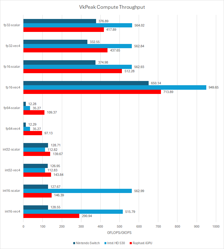
The Switch enjoys throughput comparable to Intel’s HD 530 for most basic operations. It’s also comparable for special operations like inverse square roots. Intel pulls ahead for integer multiplication performance, though that’s not likely to make a difference for games.
As mentioned earlier, Tegra X1’s Maxwell gets hardware FP16 support. Two FP16 values can be packed into the lower and upper halves of a 32-bit register. If the compiler can pull that off, FP16 can execute at double rate. Unfortunately, Nvidia’s compiler wasn’t able to do FP16 packing. AMD and Intel do enjoy double rate FP16 execution. AMD’s FP16 execution scheme works the same way and also requires packing, so it’s a bit weird that Nvidia misses out.
However, we can verify the Switch’s increased FP16 throughput with vkpeak. Vkpeak focuses on peak throughput with fused multiply add operations, and can achieve higher FP16 throughput when using 4-wide vectors.
Even with higher FP16 throughput, the Switch falls behind Intel and AMD’s basic desktop integrated GPUs. Tegra X1 does give a good account of itself with 16-bit integer operations. However I expect games to stick with FP32 or FP16, with 32-bit integers used for addressing and control flow.
Vulkan Compute Performance (VkFFT)
VkFFT uses the Vulkan API to compute Fast Fourier Transforms. Here, we’re looking at the first set of subtests (VkFFT FFT + iFFT C2C benchmark 1D batched in single precision). The first few subtests appear very memory bandwidth bound on the RX 6900 XT, and I expect similar behavior on these smaller GPUs.
Intel’s lead in subtests 3 through 11 likely comes from a memory bandwidth advantage. HD 530’s DDR4-2133 isn’t great by modern standards, but a 128-bit memory bus is better than the 64-bit LPDDR4 memory bus on the Switch.
VkFFT outputs estimated bandwidth figures alongside scores. Some of the later subtests may not be bandwidth bound, as the bandwidth figures are far below theoretical. But Intel’s HD 530 still pulls ahead, likely thanks to its higher compute throughput.
CPU to GPU Uplink Performance
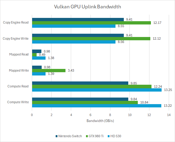
Integrated GPUs typically can’t compete with larger discrete cards in compute performance or memory bandwidth. But they can compare well in terms of how fast the CPU and GPU can communicate because discrete cards are constrained by a relatively low bandwidth PCIe interface.
The Nintendo Switch’s Tegra X1 enjoys decent bandwidth between the CPU and GPU memory spaces, and is likely held back by how fast the CPU can access memory. However, it loses in absolute terms to Nvidia’s GTX 980 Ti. Against the Tegra X1’s limited memory bandwidth, a 16x PCIe 3.0 interface can still compare well. Intel’s HD 530 turns in a similar performance when using the copy engine. But moving data with compute shaders provides a nice uplift, giving Intel the edge against the Switch.
Final Words
Tegra X1 shows the challenge of building a GPU architecture that scales across a wide range of power targets. Maxwell was built for big GPUs and has a large basic building block. Maxwell implementations can only be scaled 128 lanes at a time. Contrast that with Intel’s iGPU architecture, which can scale 8 lanes at a time by varying the number of scheduler partitions within a subslice. The equivalent in Nvidia’s world would be changing the number of scheduler partitions in a SM, changing GPU size 32 lanes at a time. Of course, Maxwell can’t do that. Adjusting GPU size 128 lanes at a time is totally fine when your GPU has over 2K lanes. With a GPU that’s just 256 lanes wide, Nvidia has their hands tied in how closely they can fit their targets.
On the Switch, Nintendo likely thought Nvidia’s default targets were a bit too high on the power and performance curve. The Switch runs Tegra X1’s iGPU at 768 MHz even though Nvidia’s documents suggest 1000 MHz should be typical. I wonder if the Switch would do better at 1000 MHz with a hypothetical 192 lane Maxwell implementation. Higher GPU clocks would improve performance for fixed function graphics blocks like rasterizers and render output units, even if theoretical compute throughput is similar. A smaller, faster clocked GPU would also require lower occupancy to exercise all of its execution units, though that’s unlikely to be a major issue because the Switch’s iGPU is so small already.
In terms of absolute performance, the Switch delivers a decent amount of graphics performance within a low power envelope. However, seeing a bog standard desktop iGPU win over a graphics-oriented console chip is eye opening. Even more eye opening is that developers are able to get recent AAA games ported to the Switch. Intel’s ubiquitous Skylake GT2 iGPU is often derided as being inadequate for serious gaming. Internet sentiment tends to accept leaving GPUs like the HD 530 behind in pursuit of better effects achieved on higher end cards.
Nintendo’s Switch shows this doesn’t have to be the case. If developers can deliver playable experiences on the Switch, they likely can do so with a HD 530 too. No doubt such optimizations require effort but carrying them out may be worth the reward of making PC gaming more accessible. Younger audiences in particular may not have the disposable income necessary to purchase current discrete cards, especially as GPU price increases at every market segment have outpaced inflation.
If you like our articles and journalism, and you want to support us in our endeavors, then consider heading over to our Patreon or our PayPal if you want to toss a few bucks our way. If you would like to talk with the Chips and Cheese staff and the people behind the scenes, then consider joining our Discord.
References
Data Sheet Nvidia Tegra X1 Series Processors, Maxwell GPU + ARM v8
Programmer’s Reference Manual, For the 2015 – 2016 Intel Core™ Processors, Celeron™ Processors and Pentium™ Processors based on the “Skylake” Platform, Volume 4: Configurations
The Compute Architecture of Intel Processor Graphics Gen9
Whitepaper Nvidia Tegra X1, Nvidia’s New Mobile Superchip


