
Microbenchmarking Chipsets for Giggles
Who cares, it's fun

Motherboard chipsets have taken on fewer and fewer performance critical functions over time. In the Athlon 64 era, integrated memory controllers took the chipset out of the DRAM access path. In the early 2010s, CPUs like Intel’s Sandy Bridge brought PCIe lanes onto the CPU, letting it interface with a GPU without chipset involvement. Chipsets today still host a lot of important IO capabilities, but they’ve become a footnote in the performance equation. Benchmarking a chipset won’t be useful, but a topic doesn’t have to be useful in order to be fun. And I do think it’ll be fun to test chipset latency.
Testing the Chipset
I’m using Nemes’s Vulkan-based GPU benchmark suite here, but with some modifications that let me allocate memory with the VK_MEMORY_PROPERTY_HOST_COHERENT_BIT set, and the VK_MEMORY_PROPERTY_DEVICE_LOCAL_BIT unset. That gives me a buffer allocated out of host memory. Then, I can run the Vulkan latency test against host memory, giving me GPU memory access latency over PCIe. The GPU in play doesn’t matter here, because I’m concerned with latency differences between using CPU PCIe slots and the southbridge ones. I’m using Nvidia’s T1000 because it’s a single slot card and can fit into the bottom PCIe slot in my various systems. All of the systems below run Windows 10, except for the FX-8350 system, which I have running Windows Server 2016. I’m using the latest drivers available for those operating systems, which would be 553.50 on Windows 10 and 475.14 on Windows Server 2016.
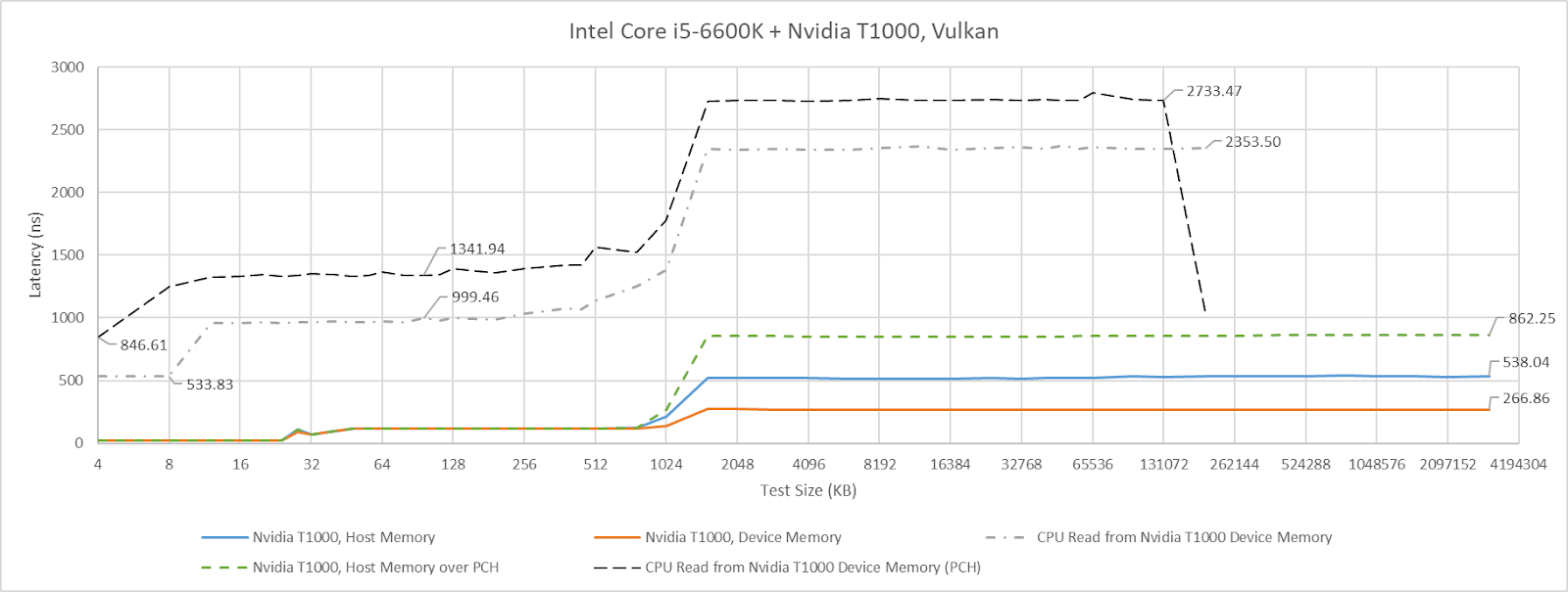
I also tried testing in the other direction by having the CPU access GPU device memory. Nemes actually does that for her Vulkan uplink latency test. However, I hit unexplainable inflection points when testing across a range of test sizes. Windows performance metrics indicated a ton of page faults at larger test sizes, perhaps hinting at driver intervention. Investigating that is a rabbit hole I don’t want to go down, and the CPU to VRAM access behavior I observed with the T1000 didn’t apply in the same way across different GPUs. I’ll therefore be focusing on GPU to host memory access latency, though I’ll leave a footnote at the end for CPU-side results.
Cache Bandwidth and Probes
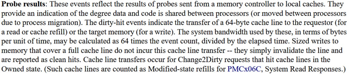
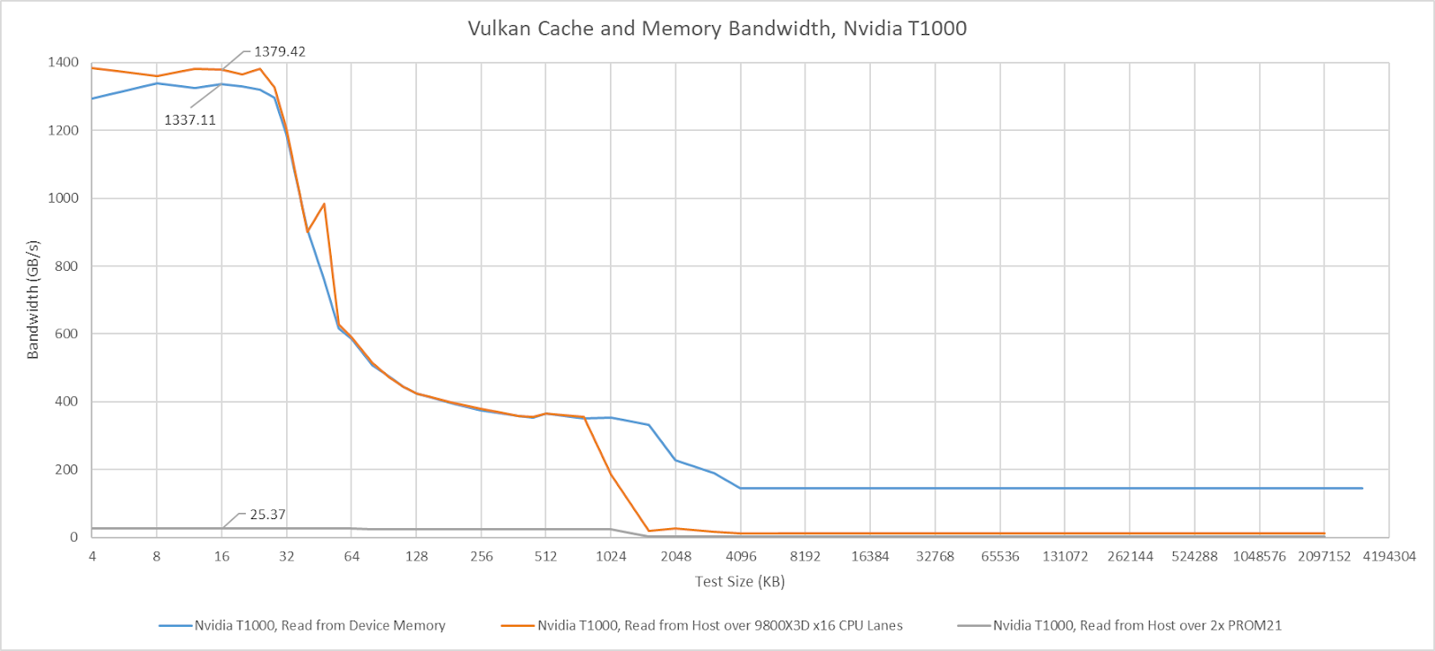
Setting the VK_MEMORY_PROPERTY_HOST_COHERENT_BIT means writes can be made visible between the CPU and GPU without explicit cache flush and invalidate commands. With the T1000, this has the strange side effect of causing a lot of probe traffic even when the GPU hits its own caches. GPU cache hit bandwidth can be constrained depending on platform configuration, possibly depending on probe throughput. AMD’s old Piledriver CPU has northbridge performance events that can track probe results. These events show a flood of probes when the test goes through small sizes that fit within the T1000’s caches. Probe activity dips when the test reaches larger sizes and bandwidth is constrained by the PCIe link.
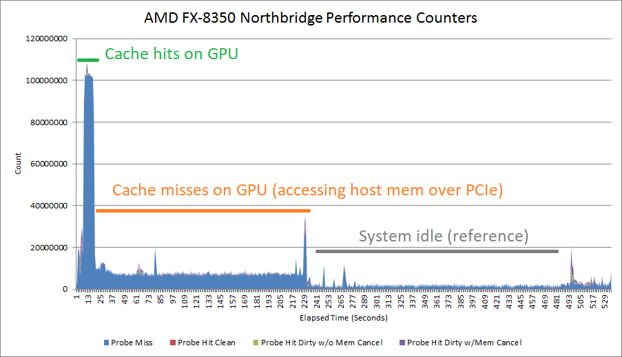
There’s a lot of mysteries here. Probes work at cacheline granularity, and AMD’s 15h BKDG makes that clear. But probe rate suggests the T1000 is initiating a probe for every 512 bytes of cache hits, not every 64. Another mystery is why cache hit latency appears unaffected.
Mysteries aside, I’ll be dropping a note when GPU cache hit bandwidth appears to be affected by the platform. But I won’t comment on GPU cache miss bandwidth, which will obviously be limited by PCIe bandwidth. The T1000 has a x16 PCIe Gen 3 interface to the host, and the newest platforms I test here can support PCIe Gen 4 or Gen 5. I don’t have a single slot card with PCIe Gen 4 or Gen 5 support.
AMD’s AM5 Platform
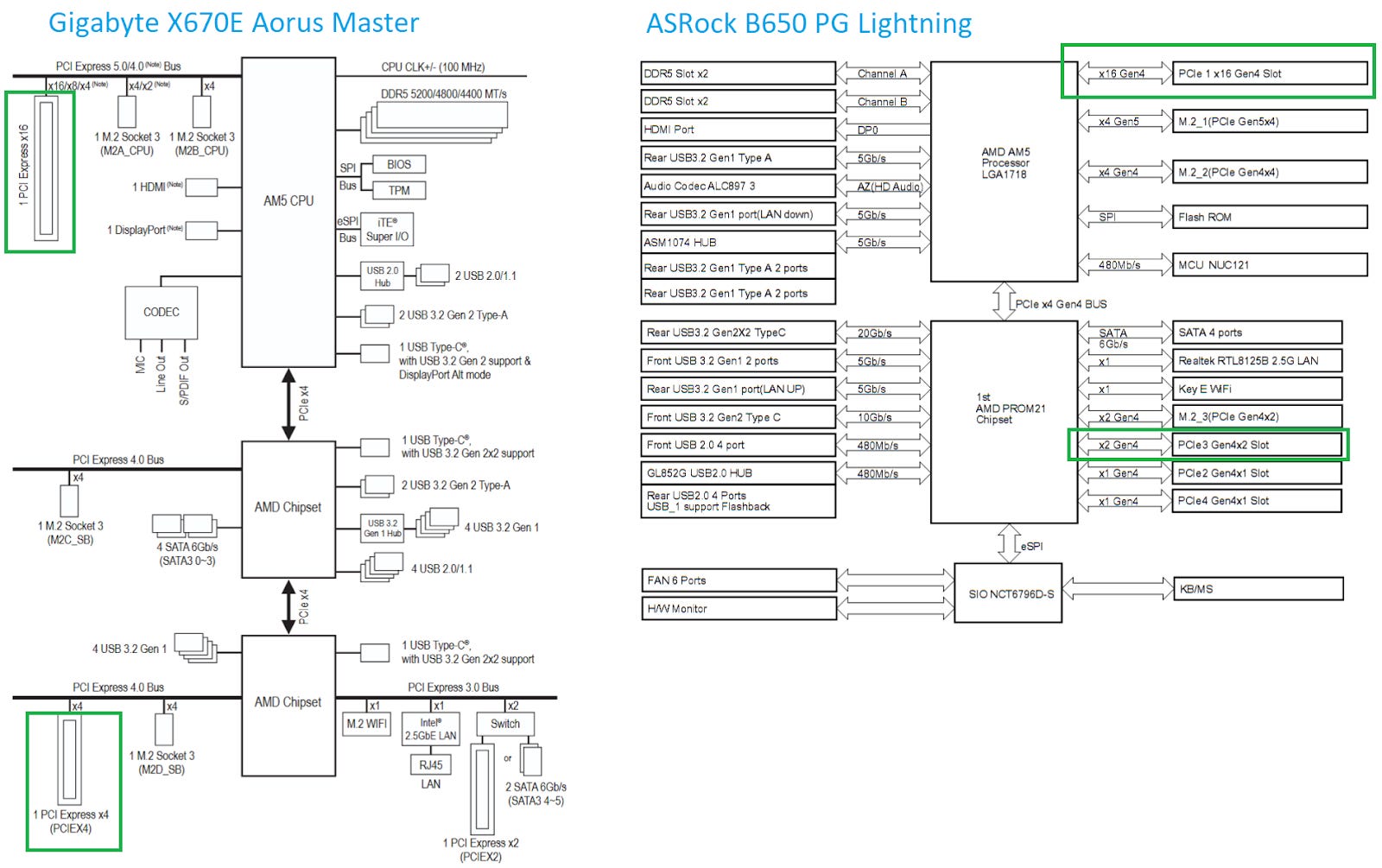
AMD’s latest desktop platform is built around the PROM21 chip. PROM21 has a PCIe 4.0 x4 uplink, and exposes a variety of downstream IO including more PCIe 4.0 links. AMD’s X670E chipset chains two PROM21 chips together, basically giving the platform two southbridge chips for better connectivity. Gigabyte’s X670E Aorus Master has three PCIe slots. One connects to the CPU, while the two others connect to the lower PROM21 chip. The PROM21 chip connected to the CPU isn’t hooked up to any PCIe slots. Instead, it’s only used to provide M.2 slots and some USB ports. The B650 chipset, tested here on the ASRock B650 PG Lightning, only uses one PROM21 chip and connects it to PCIe slots.
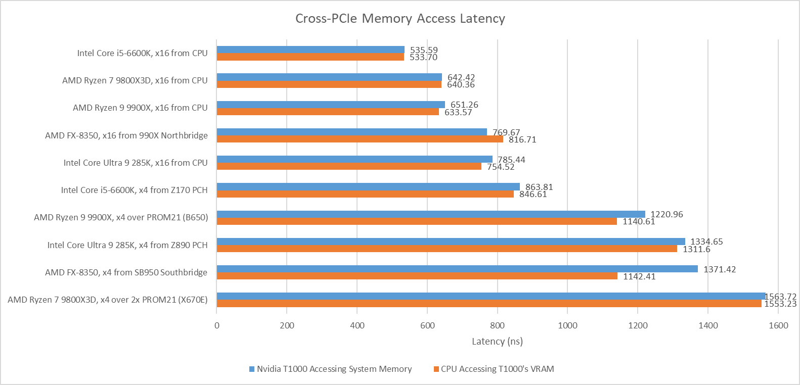
Using the CPU’s PCIe lanes gives about 650 ns of baseline latency. Going through one PROM21 chip on the B650 chipset brings latency to 1221 ns, or 569.7 ns over the baseline. On X670E, hopping over two PROM21 chips brings latency to 921.3 ns over the baseline. Going over the chipset therefore comes with a hefty latency penalty. Going through an extra PROM21 chip further increases latency.
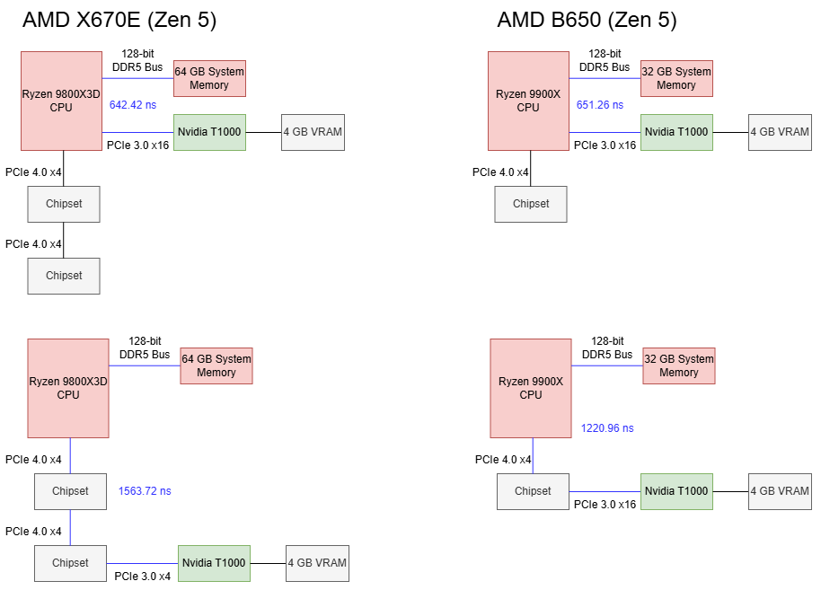
I saw no difference in GPU cache hit bandwidth with the T1000 connected to Zen 5’s CPU lanes. Switching the GPU to the chipset lanes dropped cache hit bandwidth to just above 25 GB/s, and that figure remains similar regardless of whether one or two PROM21 chips sat between the CPU and GPU.
Intel’s Arrow Lake Platform
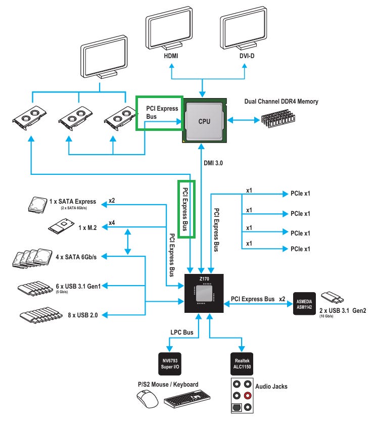
Arrow Lake chipsets follow the same topology as Intel chipsets going back to Sandy Bridge. A Platform Controller Hub (PCH) serves the southbridge role. The PCH connects to the CPU via a Direct Media Interface (DMI), which is a PCIe-like interface. Z890 uses DMI Gen 4, which can use transfer speeds of up to 16 GT/s with eight lanes. I’m testing on the MSI PRO Z890-A WIFI, which provides three PCIe slots. The first is a x16 slot connected to the CPU, while the two others are x4 slots connected to the PCH.
Baseline latency on Arrow Lake is higher than on Zen 5, with the GPU seeing 785 ns of load-to-use latency from host memory. Going through the PCH adds approximately 550 ns of latency, which is in line with what one PROM21 chip adds on the AM5 platform.
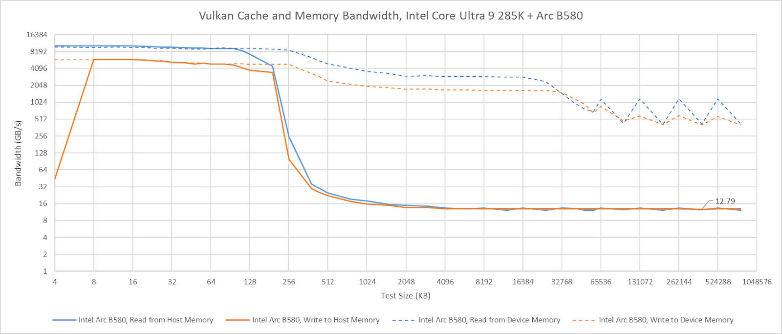
I’m going to skip commenting about the T1000’s cache hit bandwidth on Arrow Lake. It does not behave as expected, even when attached to the CPU’s PCIe lanes. The T1000’s cache hit behavior also differs from that of other GPUs. For example, Intel’s Arc B580 maintains full cache hit bandwidth when attached to the Arrow Lake platform, though curiously it can’t cache host memory in its L2.
Intel’s Skylake Platform
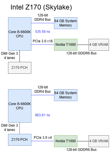
Skylake’s Z170 chipset uses a familiar southbridge-only topology like Z890, but with less connectivity and lower bandwidth. I’m testing on the MSI Z170 Gaming Pro Carbon, which connects the top PCIe x16 slot to the CPU. A middle slot also connects to the CPU to allow splitting the CPU’s 16 PCIe lanes into two sets of eight. The bottom slot connects to the PCH.
Skylake’s CPU PCIe lanes provide excellent baseline latency at 535.59 ns, while going through the Z170 PCH adds 338 ns of latency. That’s high compared to regular DRAM access latency, but compares well against current generation desktop platforms.
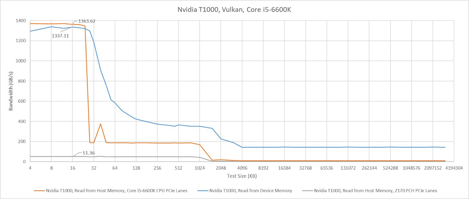
L1 bandwidth on the T1000 isn’t affected when the GPU is attached to CPU PCIe lanes, though L2 hit bandwidth is strangely lower (though still well above VRAM bandwidth). Switching the card to the Z170’s PCH lanes reduces cache hit bandwidth to just over 51 GB/s.
AMD’s AM3+ Platform
AMD’s Bulldozer and Piledriver chipsets use an older setup where the CPU has an integrated memory controller, but the chipset is still responsible for all PCIe connectivity. I’m testing on the ASUS M5A99X EVO R2.0, which implements the 990X chipset. The RD980 (990X) northbridge connects to the CPU via a 5.3 GT/s HyperTransport link, which I assume is running in 16-bit wide “ganged” mode. Two PCIe slots on the M5A99X connect to the RD980, and can run in either single x16 or 2x8 mode. A x4 A-Link Express III interface connects the northbridge to the SB950 southbridge, which provides more PCIe lanes and slower IO. A-Link Express is based on PCIe Gen 2, and runs at 5 GT/s.
Baseline latency is very acceptable at 769.67 ns when using the 990X northbridge’s PCIe lanes, which puts it between AMD’s Zen 5 and Intel’s Arrow Lake platforms. That’s a very good latency figure considering the AM3+ platform’s fastest PCIe lanes don’t come directly from the CPU like on modern platforms.
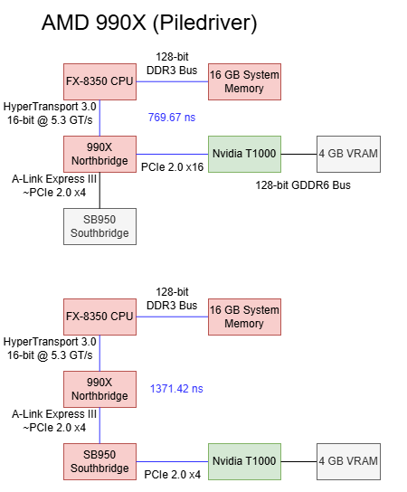
Going through the SB950 southbridge increases latency by 602 ns. It’s a higher latency increase compared to the PCH on Arrow Lake or one PROM21 chip on B650. However, southbridge latency is still better than going through two PROM21 chips on X670E.
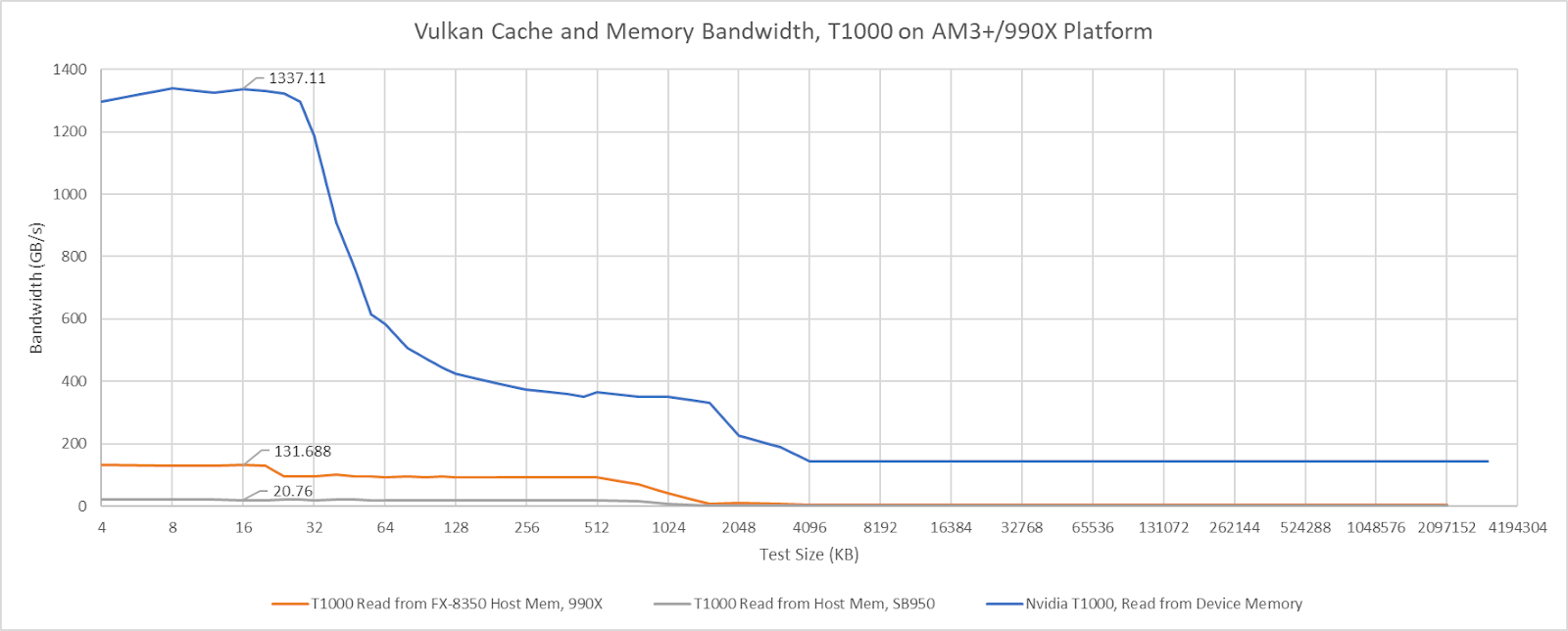
On the 990X platform, the T1000’s cache hit bandwidth is capped at around 132 GB/s when connected using the northbridge PCIe lanes. With the southbridge PCIe lanes, cache hit bandwidth drops to just over 20 GB/s. Both figures are well in excess of the platform’s IO bandwidth. The 990X’s HyperTransport lanes can only deliver 10.5 GB/s in each direction, and cache hit bandwidth far exceeds that even when the T100 is attached to the southbridge. If the T1000’s cache hit bandwidth is limited by probe throughput, then the 990X chipset has 10x more probe throughput than is necessary to saturate its IO bandwidth. Of course, that’s nowhere near enough to cover GPU cache hit bandwidth.
Sidebar: Latency from the CPU side
As mentioned before, having the CPU access GPU VRAM is another way to measure PCIe latency. Host-visible device memory allocated on the T1000 is uncacheable from the CPU side, likely to ensure coherency. If caches aren’t in play, then small test sizes provide the best estimate of baseline latency because they don’t run into address translation penalties or page faults. Here, I’m plotting CPU-to-VRAM results at the 4 KB test size next to the GPU-to-system-memory results above. There’s some difference between the two measurement methods, but not enough to paint a different picture.
Final Words
Chipsets today don’t take on performance critical roles, and accordingly aren’t optimized with low latency in mind. Going over chipset PCIe lanes adds hundreds of nanoseconds of latency, and imposes bandwidth restrictions. Chipsets can affect cache hit bandwidth too, possibly due to probe throughput constraints.
Older chipsets like AMD’s 990X show it’s possible to deliver reasonable PCIe latency even with an external northbridge. But I don’t see latency optimizations coming into play on future chipsets. With the decline of multi-GPU setups, chipsets today largely serve high latency IO like SSDs and network adapters. Those devices have latency in the microsecond range, if not milliseconds. A few hundred nanoseconds won’t make a difference. The same applies for probe performance. Accessing host-coherent memory is a corner case for GPUs, which expect to mostly work out of fast on-device memory. Needless to say, cache hits for a VRAM-backed buffer won’t require sending probes to the CPU.
I expect future chipset designs to optimize for reduced cost and better connectivity options, while keeping pace with higher bandwidth demands from newer SSDs. I don’t expect latency or probe path optimizations, though it will be interesting to keep an eye out to see if behavior changes.
Hi Chester, thanks for all the fantastic work you and the team do! In line with this article and others that you have made, I'm wondering if you would be able to create an article outlining all the main system level/macro-architecture designs that have existed in the last 20 years or so [at least at a high level]. By macro-architecture, I mean system level design such as comparing more monolithic systems such as soc's, all the way to desktop level systems which of course contain the very component you describe here in the article. The various types of interconnects that have existed over time such as xbar, ring, mesh ect and some of the main systems that have made use of them, the benefits and drawbacks of the different approaches? Also, stuff such as dma and how that differs to a more monolithic soc system where dma is less needed due to all of the system agents on the soc sharing memory access through the imc ?[to my knowledge]. I love micro-architecture, but its my belief [at least for me anyway] that knowledge of a modern system at the topology/macro-architectural level provides a lot more return on investment when it comes to understanding how modern systems work and i feel as though there isn't too much content out there that really attempts to tie all the components of the system together in a cohesive way!
Thanks Chester! Somewhat OT from chipsets, but I wonder if you might have the time and opportunity to briefly revisit Arrow Lake, specifically the 270K. Here's why: Intel claims that they were able to increase die-to-die (tile-to-tile) throughput and reduce the latencies for die-to-die traffic quite significantly.
Since Nova Lake will also be a multi-tile design, it might be interesting to see if Intel has made some meaningful progress here.
On the other hand, if you already have a Panther Lake deep dive lined up, I'll gladly table my suggestion regarding the 270K 😄. If someone at Intel is reading this, send one of your Panther Lake-based edge devices to Chester. They might be even more interesting than a notebook!