
Looking Ahead at Intel’s Xe3 GPU Architecture
Examining software changes for hints on what Intel's next GPU architecture may bring

Intel’s foray into high performance graphics has enjoyed impressive progress over the past few years, and the company is not letting up on the gas. Tom Peterson from Intel has indicated that Xe3 hardware design is complete, and software work is underway. Some of that software work is visible across several different open source repositories, offering a preview of what’s to come.
GPU Organization: Larger Render Slices?
Modern GPUs are built from a hierarchy of subdivision levels, letting them scale to hit different performance, power and price targets. A shader program running on an Intel GPU can check where it’s running by reading the low bits of the sr0 (state register 0) architectural register.
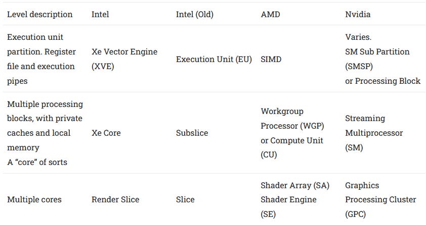
sr0 topology bits on Xe3 have a different layout1. Xe Cores within a Render Slice are enumerated with four bits, up from two in prior generations. Thus Xe3’s topology bits would be able to handle a Render Slice with up to 16 Xe Cores. Prior Xe generations could only have four Xe Cores per Render Slice, and often went right up to that. The B580 and A770 both placed four Xe Cores in each Render Slice.
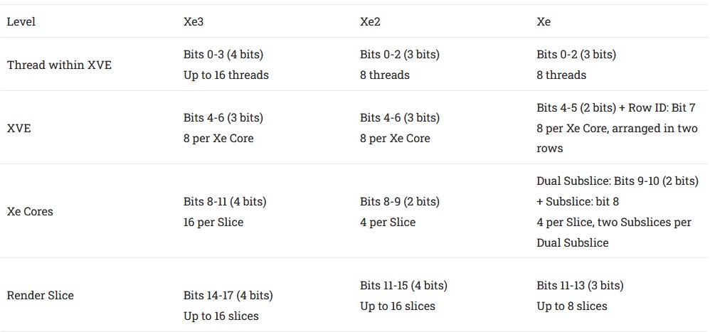
Having enough bits to describe a certain configuration doesn’t mean Intel will ship something that big. Xe did use its maximum 32 core, 4096 lane setup in the Arc A770. However, Xe2 maxed out at 20 cores and 2560 lanes with the Arc B580. Xe2’s sr0 format could theoretically enumerate 16 slices. Giving each slice the maximum of 4 Xe Cores would make a 64 Xe Core GPU with 8192 FP32 lanes. Obviously the B580 doesn’t get anywhere near that.
Xe3 goes even further. Maxing out all the topology enumeration bits would result in a ludicrously large 256 Xe Core configuration with 32768 FP32 lanes. That’s even larger than Nvidia’s RTX 5090, which “only” has 21760 FP32 lanes. Intel has been focusing on the midrange segment for a while, and I doubt we’ll see anything that big.
Instead, I think Intel wants more flexibility to scale compute power independently of fixed function hardware like ROPs and rasterizers. AMD and Nvidia’s SAs and GPCs all pack a lot more than four cores. For example, the RX 6900XT’s Shader Engines each have 10 WGPs. Nvidia’s RTX 4090 puts eight SMs in each GPC. GPUs have become more compute-heavy over time, as games use more complex shader programs. Intel seems to be following the same trend.
XVE Changes
Xe Vector Engines (XVEs) execute shader programs on Intel GPUs. They use a combination of vector-level and thread-level parallelism to hide latency.
Higher Occupancy, Increased Parallelism
Xe3 XVEs can run 10 threads concurrently, up from eight in prior generations. Like SMT on a CPU, tracking multiple threads helps a XVE hide latency using thread level parallelism. If one thread stalls, the XVE can hopefully find an un-stalled thread to issue instructions from. Active thread count is also referred to as thread occupancy. 100% occupancy on a GPU would be analogous to 100% utilization in Windows Task Manager. Unlike CPU SMT implementations, GPU occupancy can be limited by register file capacity.
Prior Intel GPUs had two register allocation modes. Normally each thread gets 128 512-bit registers, for 8 KB of registers per thread. A “large GRF” mode gives each thread 256 registers, but drops occupancy to 4 threads because of register file capacity limits. Xe3 continues to use 64 KB register files per XVE, but flexibly allocates registers in 32 entry blocks2. That lets Xe3’s XVEs get 10 threads in flight as long as each thread uses 96 or fewer registers. If a shader program needs a lot of registers, occupancy degrades more gracefully than in prior generations.
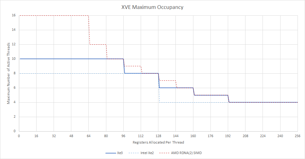
Nvidia and AMD GPUs allocate registers at even finer granularity. AMD’s RDNA 2 for example allocates registers in blocks of 16. But Xe3 is still more flexible than prior Intel generations. With this change, simple shaders that only need a few registers will enjoy better latency tolerance from more thread-level parallelism. And more complex shaders can avoid dropping to the “large GRF” mode.
Xe3’s XVEs have more scoreboard tokens too. Like AMD and Nvidia, Intel uses compiler assisted scheduling for long latency instructions like memory accesses. A long latency instruction can set a scoreboard entry, and a dependent instruction can wait until that entry is cleared. Each Xe3 thread gets 32 scoreboard tokens regardless of occupancy, so a XVE has 320 scoreboard tokens in total. On Xe2, a thread gets 16 tokens if the XVE is running eight threads, or 32 in “large GRF” mode with four threads. Thus Xe2’s XVEs only have 128 scoreboard tokens in total. More tokens let thread have more outstanding long latency instructions. That very likely translates to more memory level parallelism per thread.
“Scalar” Register (s0)
Intel’s GPU ISA has a vector register file (GRF, or General Register File) that stores much of a shader program’s data and feeds the vector execution units. It also has an “Architecture Register File” (ARF) with special registers. Some of those can store data, like the accumulator registers. But others serve special purposes. For example, sr0 as mentioned above provides GPU topology info, along with floating point exception state and thread priority. A 32-bit instruction pointer points to the current instruction address, relative to the instruction base address.
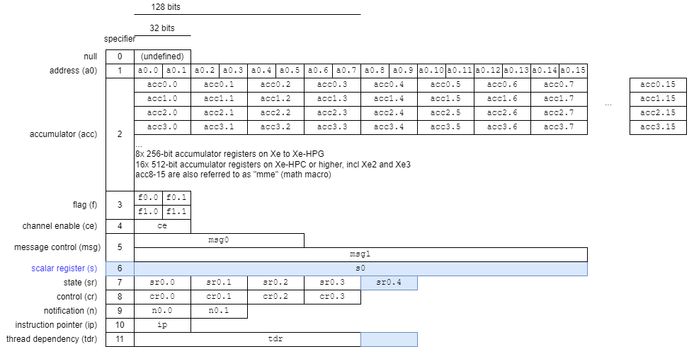
Xe3 adds a “Scalar Register” (s0) to the ARF6. s0 is laid out much like the address register (a0), and is used for gather-send instructions. XVEs access memory and communicate with other shared using by sending messages over the Xe Core’s message fabric, using send instructions. Gather-send appears to let Xe3 gather non-contiguous values from the register file, and send them with a single send instruction.
Besides adding the Scalar Register, Xe3 extends the thread dependency register (TDR) to handle 10 threads. sr0 gains an extra 32-bit doubleword for unknown reasons.
Instruction Changes
Xe3 supports a saturation modifier for FCVT, an instruction that converts between different floating point types (not between integer and floating point). FCVT was introduced with Ponte Vecchio, but the saturation modifier could ease conversion from higher to lower precision floating point formats. Xe3 also gains HF8 (half float 8-bit) format support, providing another 8-bit floating point format option next to the BF8 type already supported in Xe2.
For the XMX unit, Xe3 gains a xdpas instruction4. sdpas stands for sparse systolic dot product with accumulate5. Matrices with a lot of zero elements are known as sparse matrices. Operations on sparse matrices can be optimized because anything multiplied by zero is obviously zero. Nvidia and AMD GPUs have both implemented sparsity optimizations, and Intel is apparently looking to do the same.
Raytracing: Sub-Triangle Opacity Culling
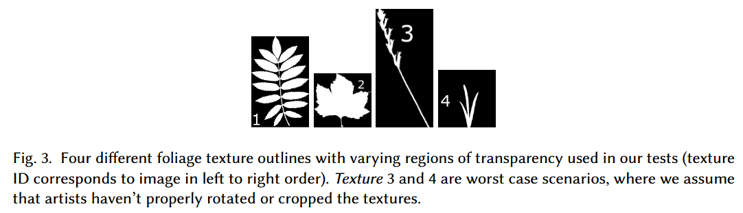
Sub-Triangle Opacity Culling (STOC) subdivides triangles in BVH leaf nodes, and marks sub-triangles as transparent, opaque, or partially transparent. The primary motivation is to reduce wasted any-hit shader work when games use texture alpha channels to handle complex geometry. Intel’s paper calls out foliage as an example, noting that programmers may use low vertex counts to reduce “rendering, animation, and even simulation run times.”7 BVH geometry from the API perspective can only be completely transparent or opaque, so games mark all partially transparent primitives as transparent. Each ray intersection will fire an any-hit shader, which carries out alpha testing. If alpha testing indicates the ray intersected a transparent part of the primitive, the shader program doesn’t contribute a sample and the any-hit shader launch is basically wasted. STOC bits let the any-hit shader skip alpha testing if the ray intersects a completely transparent or completely opaque sub-triangle.
Storing each sub-triangle’s opacity information takes two bits, so STOC does require more storage compared to using a single opacity bit for the entire triangle. Still, it’s far more practical than packing entire textures into the BVH. Intel’s paper found that a software-only STOC implementation improved performance by 5.9-42.2% compared to standard alpha tests when handling translucent ray-traced shadows.

STOC-aware raytracing hardware can provide further gains, especially with Intel's raytracing implementation. Intel's raytracing acceleration method closely aligns with the DXR 1.0 standard. A raytracing accelerator (RTA) autonomously handles traversal and launches hit/miss shaders by sending messages to the Xe Core's thread dispatcher. STOC bits could let the RTA skip shader launches if the ray intersects a completely transparent sub-triangle. For an opaque sub-triangle, the RTA can tell the shader program to skip alpha testing, and terminate the ray early.

Xe3 brings STOC bits into hardware raytracing data structures with two levels of sophistication. A basic implementation retains 64B leaf nodes, but creatively finds space to fit 18 extra bits. Intel's QuadLeaf structure represents a merged pair of triangles. Each triangle gets 8 STOC bits, implying four sub-triangles. Another two bits indicate whether the any-hit shader should do STOC emulation in software, potentially letting programmers turn off hardware STOC for debugging. This mode is named "STOC1" in code.
A “STOC3” structure takes things further by storing pointers to STOC bits rather than embedding them into the BVH. That allows more flexibility in how much storage the STOC bits can use. STOC3 also specifies recursion levels for STOC bits, possibly for recursively partitioning triangles. Subdividing further would reduce the number of partially transparent sub-triangles, which require alpha testing from the any-hit shader. Storing pointers for STOC3 brings leaf node size to 128 bytes, increasing BVH memory footprint.
Possible performance gains are exciting, but using STOC requires work from game developers or game engines. Intel suggests that STOC bits can be generated offline as part of game asset compilation. Artists will have to determine whether using STOC will provide a performance uplift for a particular scene. A scene with a lot of foliage might benefit massively from STOC. A chain link fence may be another story. STOC isn’t a part of the DirectX or Vulkan standards, which can be another obstacle to adoption. However, software-only STOC can still provide benefits. That could encourage developers to try it out. If they do implement it, STOC-aware Xe3 hardware stands to gain more than a software-only solution.
Final Words
We’re still some time away from real Xe3 products. But software changes suggest Xe3 is another significant step forward for Intel’s graphics architecture. Xe2 was a solid step in Intel’s foray into discrete graphics, providing better performance than Xe with a nominally smaller GPU. Xe3 tweaks the architecture again and likely has similar goals. Higher occupancy and dynamic register allocation would make Xe Cores more latency tolerant, improving utilization. Those changes also bring Intel’s graphics architecture closer to AMD and Nvidia’s.
XVE changes show Intel is still busy evolving their core compute architecture. In contrast, Nvidia’s Streaming Multiprocessors haven’t seen significant changes from Ampere to Blackwell. Nvidia may have felt Ampere’s SM architecture was good enough, and turned their efforts to tuning features while scaling up the GPU to keep providing generational gains. Intel meanwhile seeks to get more out of each Xe Core (and Xe2 achieved higher performance than Xe with fewer Xe Cores).
In a similarity with Nvidia, Intel is pushing hard on the features front and evidently has invested into research. GPUs often try to avoid doing wasted work. Just rasterization pipelines use early depth testing to avoid useless pixel shader invocations, STOC avoids spawning useless any-hit shaders. It’s too early to tell what kind of difference STOC or other Xe3 features will make. But anyone doubting Intel’s commitment to moving their GPU architecture forward should take a serious look at Mesa and Intel Graphics Compiler changes. There’s a lot going on, and I look forward to seeing Xe3 whenever it’s ready.
can't see footnotes of the article!
Great article!
But i still don't quite understand what's new about rdna 4 "out of order memory". Could you go into more detail about this rdna 4 feature in the rx 9070 article?
Thank you very much!