
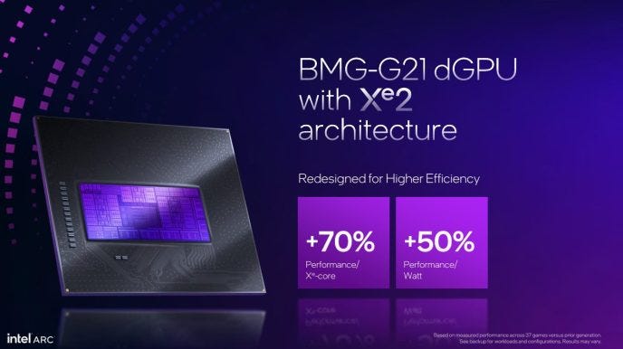
Intel’s Battlemage Architecture

Intel’s Alchemist architecture gave the company a foot in the door to the high performance graphics segment. The Arc A770 proved to be a competent first effort, able to run many games with credible performance. Now, Intel is passing the torch to a new graphics architecture, named Battlemage.
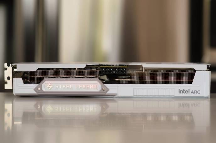
Like Alchemist, Battlemage targets the midrange segment. It doesn’t try to compete with AMD or Nvidia’s high end cards. While it’s not as flashy as Nvidia’s RTX 4090 or AMD’s RX 7900 XTX, midrange GPUs account for a much larger share of the discrete GPU market, thanks to their lower prices. Unfortunately, today’s midrange cards like the RTX 4060 and RX 7600 only come with 8 GB of VRAM, and are poor value. Intel takes advantage of this by launching the Arc B580 at $250, undercutting both competitors while offering 12 GB of VRAM.
For B580 to be successful, its new Battlemage architecture has to execute well across a variety of graphics workloads. Intel has made numerous improvements over Alchemist, aiming to achieve better performance with less compute power and less memory bandwidth. I’ll be looking at the Arc B580, with comparison data from the A770 and A750, as well as scattered data I have lying around.
System Architecture
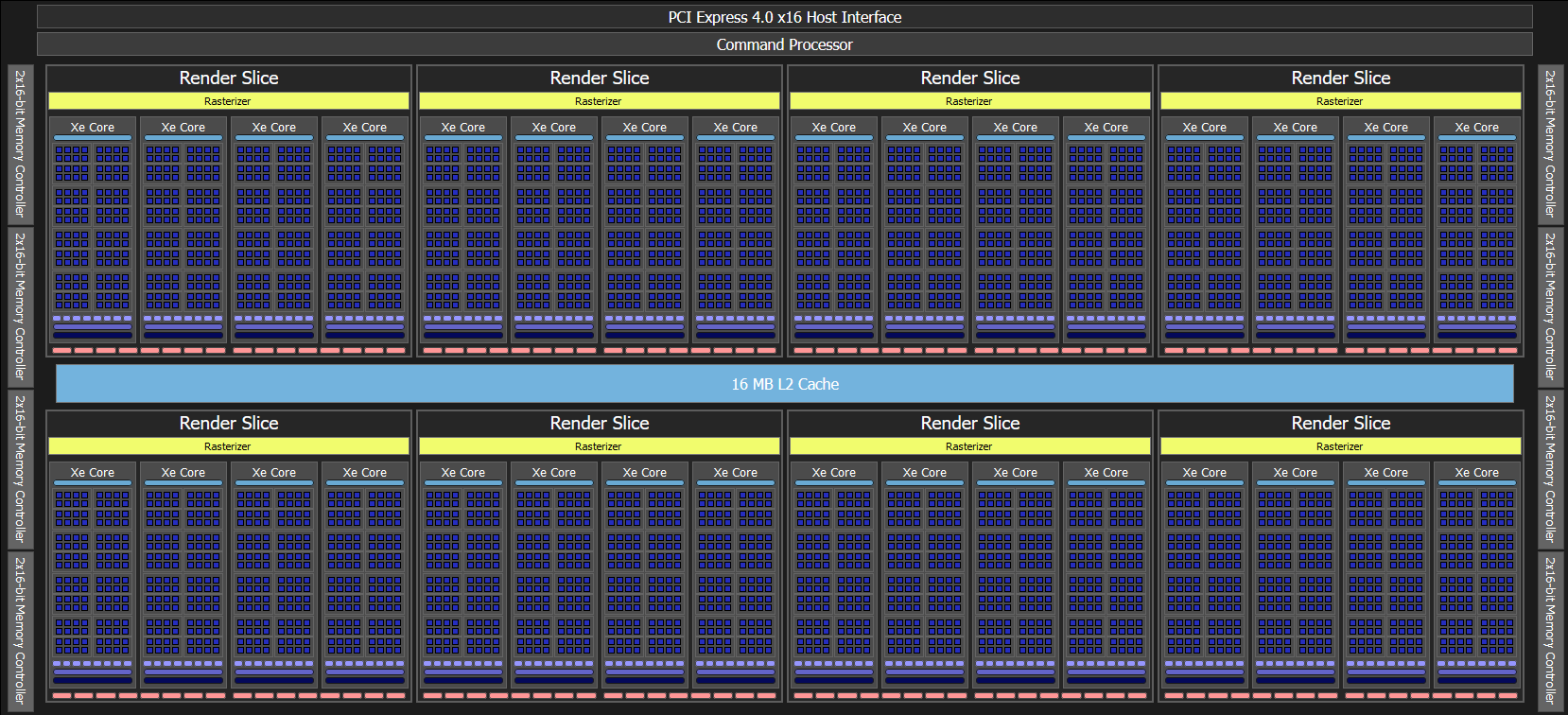
Battlemage is organized much like its predecessor. Xe Cores continue to act as a basic building block. Four Xe Cores are grouped into a Render Slice, which also contains render backends, a rasterizer, and associated caches for those fixed function units. The entire GPU shares an 18 MB L2 cache.

The Arc B580 overall is a smaller GPU than its outgoing Alchemist predecessors. B580 has five Render Slices to A770’s eight. In total, B580 has 2560 FP32 lanes to A770’s 4096.
Battlemage launches with a smaller memory subsystem too. The B580 has a 192-bit GDDR6 bus running at 19 GT/s, giving it 456 GB/s of theoretical bandwidth. A770 has 560 GB/s of GDDR6 bandwidth, thanks to a 256-bit bus running at 17.5 GT/s.
Even the host interface has been cut down. B580 only has a PCIe 4.0 x8 link, while A770 gets a full size x16 one. Intel’s new architecture has a lot of heavy lifting to do if it wants to beat a much larger implementation of its predecessor.
Battlemage’s Xe Cores
Battlemage’s architectural changes start at its Xe Cores. The most substantial changes between the two generations actually debuted on Lunar Lake. Xe Cores are further split into XVEs, or Xe Vector engines. Intel merged pairs of Alchemist XVEs into ones that are twice as wide, completing a transition towards larger execution unit partitions. Xe Core throughput stays the same at 128 FP32 operations per cycle.
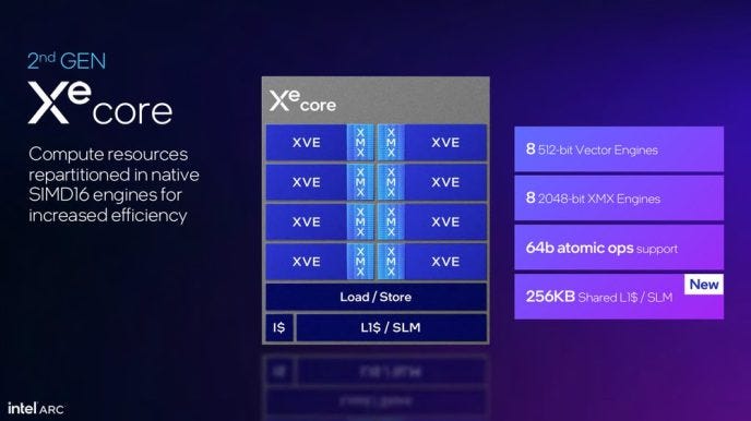
A shared instruction cache feeds all eight XVEs in a Xe Core. Alchemist had a 96 KB instruction cache, and Battlemage almost certainly has an instruction cache at least as large. Instructions on Intel GPUs are generally 16 bytes long, with a 8 byte compacted form in some cases. A 96 KB instruction cache therefore has a nominal capacity of 6-12K instructions.
Xe Vector Engines (XVEs)
XVEs form the smallest partition in Intel GPUs. Each XVE tracks up to eight threads, switching between them to hide latency and keep its execution units fed. A 64 KB register file stores thread state, giving each thread up to 8 KB of registers while maintaining maximum occupancy. Giving a register count for Intel GPUs doesn’t really work, because Intel GPU instructions can address the register file with far more flexibility than Nvidia or AMD architectures. Each instruction can specify a vector width, and access a register as small as a single scalar element.
For most math instructions, Battlemage sticks with 16-wide or 32-wide vectors, dropping the SIMD8 mode that could show up with Alchemist. Vector execution reduces instruction control overhead because a single operation gets applied across all lanes in the vector. However, that results in lost throughput if some lanes take a different branch direction. On paper, Battlemage’s longer native vector lengths would make it more prone to suffering such divergence penalties. But Alchemist awkwardly shared control logic between XVE pairs, making SIMD8 act like SIMD16, and SIMD16 act a lot like SIMD64 aside from a funny corner case (see the Meteor Lake article for more on that).
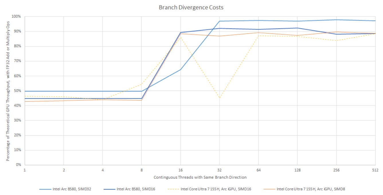
Battlemage’s divergence behavior by comparison is intuitive and straightforward. SIMD16 achieves full utilization if groups of 16 threads go the same way. The same applies for SIMD32 and groups of 32 coherent threads. Thus Battlemage is actually more agile than its predecessor when dealing with divergent branches, while enjoying the efficiency advantage of using larger vectors.

Like Alchemist, Battlemage executes most math operations down two ports (ALU0, ALU1). ALU0 handles basic FP32 and FP16 operations, while ALU1 handles integer math and less common instructions. Intel’s port layout has parallels to Nvidia’s Turing, which also splits dispatch bandwidth between 16-wide FP32 and INT32 units. A key difference is that Turing uses fixed 32-wide vectors, and keeps both units occupied by feeding them on alternate cycles. Intel can issue instructions of the same type back-to-back, and can select multiple instructions to issue per cycle to different ports.
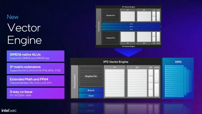
In another similarity to Turing, Battlemage carries forward Alchemist’s “XMX” matrix multiplication units. Intel claims 3-way co-issue, implying XMX is on a separate port. However, VTune only shows multiple pipe active metrics for ALU0+ALU1 and ALU0+XMX. I’ve drawn XMX as a separate port above, but the XMX units could be on ALU1.

Gaming workloads tend to use more floating point operations. During compute heavy sections, ALU1 offloads other operations and keeps ALU0 free to deal with floating point math. XeSS exercises the XMX unit, with minimal co-issue alongside vector operations. A generative AI workload shows even less XMX+vector co-issue.

As expected for any specialized execution unit, XMX software support is far from guaranteed. Running AI image generation or language models using other frameworks heavily exercises B580’s regular vector units, while leaving the XMX units idle.
In microbenchmarks, Intel’s older A770 and A750 can often use their larger shader arrays to achieve higher compute throughput than B580. However, B580 behaves more consistently. Alchemist had trouble with FP32 FMA operations. Battlemage in contrast has no problem getting right up to its theoretical throughput. FP32+INT32 dual issue doesn’t happen perfectly on Battlemage, but it barely happened at all on A750.

On the integer side, Battlemage is better at dealing with lower precision INT8 operations. Using Meteor Lake’s iGPU as a proxy, Intel’s last generation architecture used mov and add instruction pairs to handle char16 adds, while Battlemage gets it done with just an add.

Each XVE also has a branch port for control flow instructions, and a “send” port that lets the XVE talk with the outside world. Load on these ports is typically low, because GPU programs don’t branch as often as CPU ones, and shared functions accessed through the “send” port won’t have enough throughput to handle all XVEs hitting it at the same time.
Memory Access
Battlemage’s memory subsystem has a lot in common with Alchemist’s, and traces its origins to Intel’s integrated graphics architectures over the past decade. XVEs access the memory hierarchy by sending a message to the appropriate shared functional unit. At one point, the entire iGPU was basically the equivalent of a Xe Core, with XVE equivalents acting as basic building blocks. XVEs would access the iGPU’s texture units, caches, and work distribution hardware over a messaging fabric. Intel has since built larger subdivisions, but the terminology remains.
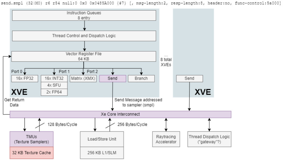
Texture Path
Each Xe Core has eight TMUs, or texture samplers in Intel terminology. The samplers have a 32 KB texture cache, and can return 128 bytes/cycle to the XVEs. Battlemage is no different from Alchemist in this respect. But the B580 has less texture bandwidth on tap than its predecessor. Its higher clock speed isn’t enough to compensate for having far fewer Xe Cores.

B580 runs at higher clock speeds, which brings down texture cache hit latency too. In clock cycle terms though, Battlemage has nearly identical texture cache hit latency to its predecessor. L2 latency has improved significantly, so missing the texture cache isn’t as bad on Battlemage.

Data Access (Global Memory)
Global memory accesses are first cached in a 256 KB block, which serves double duty as Shared Local Memory (SLM). It’s larger than Alchemist and Lunar Lake’s 192 KB L1/SLM block, so Intel has found the transistor budget to keep more data closer to the execution units. Like Lunar Lake, B580 favors SLM over L1 capacity even when a compute kernel doesn’t allocate local memory.

Intel may be able to split the L1/SLM block in another way, but a latency test shows exactly the same result regardless of whether I allocate local memory. Testing with Nemes’s Vulkan test suite also shows 96 KB of L1.

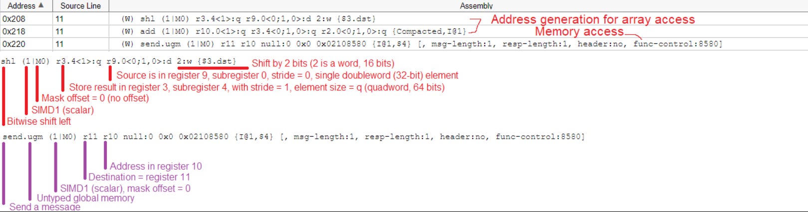
Global memory access on Battlemage offers lower latency than texture accesses, even though the XVEs have to handle array address generation. With texture accesses, the TMUs do all the address calculations. All the XVEs do is send them a message. L1 data cache latency is similar to Alchemist in clock cycle terms, though again higher clock speeds give B580 an actual latency advantage.
Scalar Optimizations?
Battlemage gets a clock cycle latency reduction too with scalar memory accesses. Intel does not have separate scalar instructions like AMD. But Intel’s GPU ISA lets each instruction specify its SIMD width, and SIMD1 instructions are possible. Intel’s compiler has been carrying out scalar optimizations and opportunistically generating SIMD1 instructions well before Battlemage, but there was no performance difference as far as I could tell. Now there is.

On B580, L1 latency for a SIMD1 (scalar) access is about 15 cycles faster than a SIMD16 access. SIMD32 accesses take one extra cycle when microbenchmarking, though that’s because the compiler generates two sets of SIMD16 instructions to calculate addresses across 32 lanes. I also got Intel’s compiler to emit scalar INT32 adds, but those didn’t see improved latency over vector ones. Therefore, the scalar latency improvements almost certainly come from an optimized memory pipeline.
SIMD1 instructions also help within the XVEs. Intel doesn’t use a separate scalar register file, but can more flexibly address their vector register file than AMD or Nvidia. Instructions can access individual elements (sub-registers) and read out whatever vector width they want. Intel’s compiler could pack many “scalar registers” into the equivalent of a vector register, economizing register file capacity.
L1 Bandwidth
I was able to get better efficiency out of B580’s L1 than A750’s using float4 loads from a small array. Intel suggests Xe-HPG’s L1 can deliver 512 bytes per cycle, but I wasn’t able to get anywhere close on either Alchemist or Battlemage. Microbenchmarking puts per-Xe Core bandwidth at a bit under 256 bytes per cycle on both architectures.

Even if the L1 can only provide 256 bytes per cycle, that still gives Intel’s Xe Core as much L1 bandwidth as an AMD RDNA WGP, and twice as much L1 bandwidth as an Nvidia Ampere SM. 512 bytes per cycle would let each XVE complete a SIMD16 load every cycle, which is kind of overkill anyway.
Local Memory (SLM)
Battlemage uses the same 256 KB block for L1 cache and SLM. SLM provides an address space local to a group of threads, and acts as a fast software managed scratchpad. In OpenCL, that’s exposed via the local memory type. Everyone likes to call it something different, but for this article I’ll use OpenCL and Intel’s term.

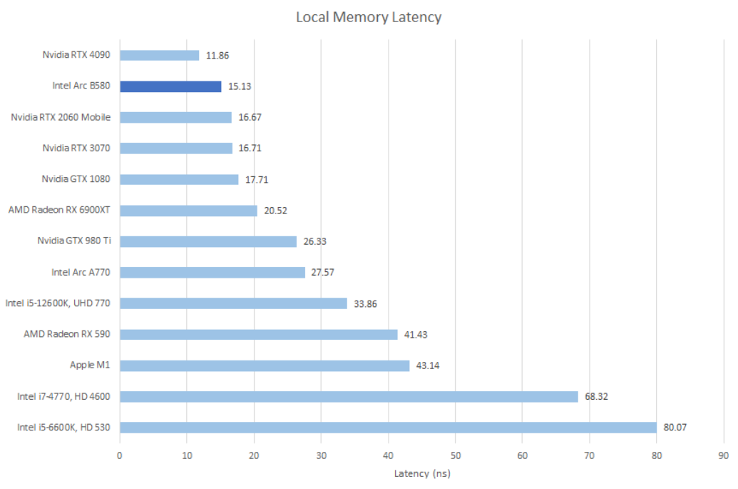
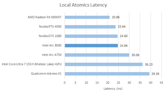
Even though both local memory and L1 cache hits are backed by the same physical storage, SLM accesses enjoy better latency. Unlike cache hits, SLM accesses don’t need tag checks or address translation. Accessing Battlemage’s 256 KB block of memory in SLM mode brings latency down to just over 15 ns. It’s faster than doing the same on Alchemist, and is very competitive against recent GPUs from AMD and Nvidia.
Local memory/SLM also lets threads within a workgroup synchronize and exchange data. From testing with atomic_cmpxchg on local memory, B580 can bounce values between threads a bit faster than its predecessor. Nearly all of that improvement is down to higher clock speed, but it’s enough to bring B580 in line with AMD and Nvidia’s newer GPUs.
Backing structures for local memory often contain dedicated ALUs for handling atomic operations. For example, the LDS on AMD’s RDNA architecture is split into 32 banks, with one atomic ALU per bank. Intel almost certainly has something similar, and I’m testing that with atomic_add operations on local memory. Each thread targets a different address across an array, aiming to avoid contention.

Alchemist and Battlemage both appear to have 32 atomic ALUs attached to each Xe Core’s SLM unit, much like AMD’s RDNA and Nvidia’s Pascal. Meteor Lake’s Xe-LPG architecture may have half as many atomic ALUs per Xe Core.
L2 Cache
Battlemage has a two level cache hierarchy like its predecessor and Nvidia’s current GPUs. B580’s 18 MB L2 is slightly larger than A770’s 16 MB L2. A770 divided its L2 into 32 banks, each capable of handling a 64 byte access every cycle. At 2.4 GHz, that’s good for nearly 5 TB/s of bandwidth.
Intel didn’t disclose B580’s L2 topology, but a reasonable assumption is that Intel increased bank size from 512 to 768 KB, keeping 4 L2 banks tied to each memory controller. If so, B580’s L2 would have 24 banks and 4.3 TB/s of theoretical bandwidth at 2.85 GHz. Microbenchmarking using Nemes’s Vulkan test gets a decent proportion of that bandwidth. Efficiency is much lower on the older A750, which gets approximately as much bandwidth as B580 despite probably having more theoretical L2 bandwidth on tap.

Besides insulating the execution units from slow VRAM, the L2 can act as a point of coherency across the GPU. B580 is pretty fast when bouncing data between threads using global memory, and is faster than its predecessor.
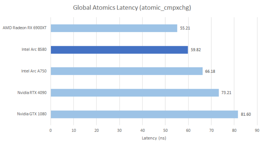
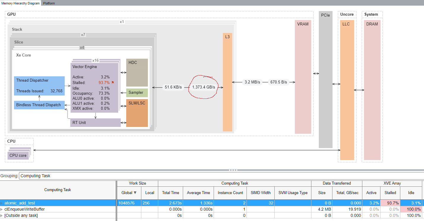
With atomic add operations on global memory, Battlemage does fine for a GPU of its size and massively outperforms its predecessor.

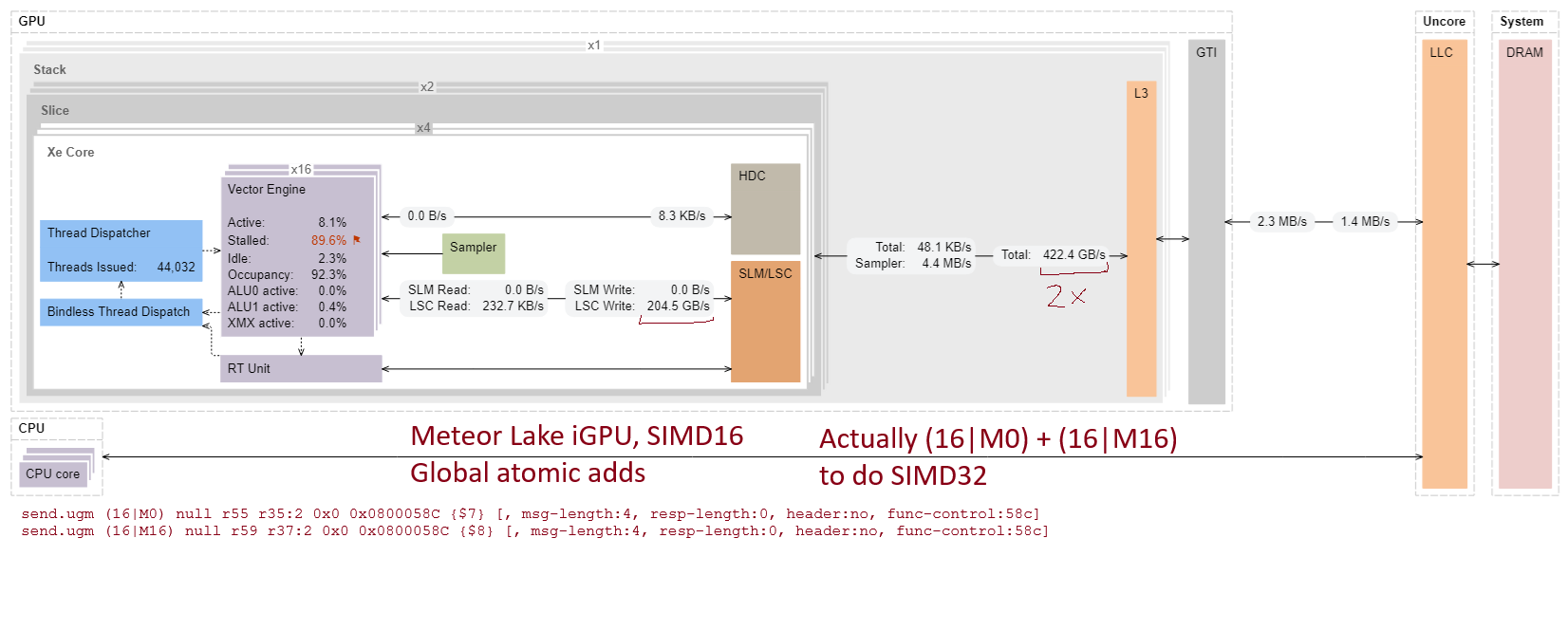
I’m using INT32 operations, so 86.74 GOPS on the A750 would correspond to 351 GB/s of L2 bandwidth. On the B580, 220.97 GOPS would require 883.9 GB/s. VTune however reports far higher L2 bandwidth on A750. Somehow, A750 sees 1.37 TB/s of L2 bandwidth during the test, or nearly 4x more than it should need.
Meteor Lake’s iGPU is a close relative of Alchemist, but its ratio of global atomic add throughput to Xe Core count is similar to Battlemage’s. VTune reports Meteor Lake’s iGPU using more L2 bandwidth than required, but only by a factor of 2x. Curiously, it also shows the expected bandwidth coming off the XVEs. I wonder if something in Intel’s cross-GPU interconnect didn’t scale well with bigger GPUs.
With Battlemage, atomics are broken out into a separate category and aren’t reported as regular L2 bandwidth. VTune indicates atomics are passed through the load/store unit to L2 without any inflation. Furthermore, the L2 was only 79.6% busy, suggesting there’s a bit of headroom at that layer.
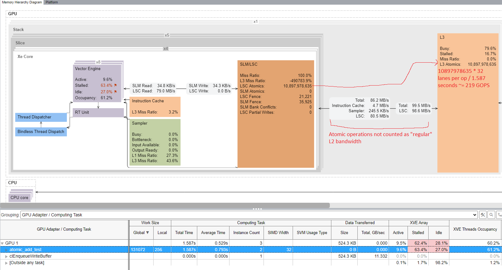
This could just be a performance monitoring improvement, but performance counters are typically closely tied to the underlying architecture. I suspect Intel made major changes to how they handle global memory atomics, letting performance scale better on larger GPUs. I’ve noticed that newer games sometimes use global atomic operations. Perhaps Intel noticed that too, and decided it was time to optimize them.
VRAM Access
B580 has a 192-bit GDDR6 VRAM subsystem, likely configured as six 2×16-bit memory controllers. Latency from OpenCL is higher than it was in the previous generation.

I suspect this only applies to OpenCL, because latency from Vulkan (with Nemes’s test) shows just over 300 ns of latency. Latency at large test sizes will likely run into TLB misses, and I suspect Intel is using different page sizes for different APIs.
Compared to its peers, the Arc B580 has more theoretical VRAM bandwidth at 456 GB/s, but also less L2 capacity. For example, Nvidia’s RTX 4060 has 272 GB/s VRAM bandwidth using a 128-bit GDDR6 bus running at 17 GT/s, with 24 MB of L2 in front of it. I profiled a few things with VTune and picked out spikes in VRAM bandwidth usage. I also checked reported L2 bandwidth over the same sampling interval.

Intel’s balance of cache capacity and memory bandwidth seems to work well, at least in the few examples I checked. Even when VRAM bandwidth demands are high, the 18 MB L2 is able to catch enough traffic to avoid pushing GDDR6 bandwidth limits. If Intel hypothetically used a smaller GDDR6 memory subsystem like Nvidia’s RTX 4060, B580 would need a larger cache to avoid reaching VRAM bandwidth limits.
PCIe Link
Probably as a cost cutting measure, B580 has a narrower PCIe link than its predecessor. Still, a x8 Gen 4 link provides as much theoretical bandwidth as a x16 Gen 3 one. Testing with OpenCL doesn’t get close to theoretical bandwidth, but B580 is at a disadvantage compared to A750.

PCIe link bandwidth often has minimal impact on gaming performance, as long as you have enough VRAM. B580 has a comparatively large 12 GB VRAM pool compared to its immediate competitors, which also have PCIe 4.0 x8 links. That could give B580 an advantage within the midrange market, but that doesn’t mean it’s immune to problems.

DCS for example will uses over 12 GB of VRAM with mods. Observing different aircraft in different areas often causes stutters on the B580. VTune shows high PCIe traffic as the GPU must frequently read from host memory.
Final Words
Battlemage retains Alchemist’s high level goals and foundation, but makes a laundry list of improvements. Compute is easier to utilize, cache latency improves, and weird scaling issues with global memory atomics have been resolved. Intel has made some surprising optimizations too, like reducing scalar memory access latency. The result is impressive, with Arc B580 easily outperforming the outgoing A770 despite lagging in nearly every on-paper specification.
Some of Intel’s GPU architecture changes nudge it a bit closer to AMD and Nvidia’s designs. Intel’s compiler often prefers SIMD32, a mode that AMD often chooses for compute code or vertex shaders, and one that Nvidia exclusively uses. SIMD1 optimizations create parallels to AMD’s scalar unit or Nvidia’s uniform datapath. Battlemage’s memory subsystem emphasizes caching more than its predecessor, while relying less on high VRAM bandwidth. AMD’s RDNA 2 and Nvidia’s Ada Lovelace made similar moves with their memory subsystems.
Of course Battlemage is still a very different animal from its discrete GPU competitors. Even with larger XVEs, Battlemage still uses smaller execution unit partitions than AMD or Nvidia. With SIMD16 support, Intel continues to support shorter vector widths than the competition. Generating SIMD1 instructions gives Intel some degree of scalar optimization, but stops short of having a full-out scalar/uniform datapath like AMD or post-Turing Nvidia. And 18 MB of cache is still less than the 24 or 32 MB in Nvidia and AMD’s midrange cards.
Differences from AMD and Nvidia aside, Battlemage is a worthy step on Intel’s journey to take on the midrange graphics market. A third competitor in the discrete GPU market is welcome news for any PC enthusiast. For sure, Intel still has some distance to go. Driver overhead and reliance on resizable BAR are examples of areas where Intel is still struggling to break from their iGPU-only background.
But I hope Intel goes after higher-end GPU segments once they’ve found firmer footing. A third player in the high end dGPU market would be very welcome as many folks are still on Pascal or GCN due to folks feeling as if there is not a reasonable upgrade yet. Intel’s Arc B580 addresses some of that pent-up demand, at least when it’s not out-of-stock. I look forward to seeing Intel’s future GPU efforts.
If you like the content then consider heading over to the Patreon or PayPal if you want to toss a few bucks to Chips and Cheese. Also consider joining the Discord.
I am missing some ray tracing analysis. Maybe later comparing Intel, AMD and Nvidia? Anyway thank you for the article.
Thank you for the broadcast, as well. It helped me to understand some of the use cases for XMx (XeSS upscaling in Cyberpunk) and INT64 and memory access. You guys rock.