Inside the Snapdragon 855’s iGPU
Qualcomm’s Adreno 6xx architecture has been superseded Adreno 7xx, but it’s still used in countless devices, including the current-gen Snapdragon 8cx Gen 3. Here, I’ll be looking at the Adreno 640 GPU in the Snapdragon 855. Zarif98 on Reddit kindly provided a OnePlus 7 Pro, and I’ll be using that to check out Adreno 640.
Compared to the older Snapdragon 821’s Adreno 530, Adreno 640 dramatically increases compute throughput while still working within a very constrained power and thermal envelope. Process node improvements help, and TSMC’s 7 nm process should be far better than the 14 nm Samsung node used in the Snapdragon 821. But cell phone SoC constraints meant Qualcomm couldn’t go around copy-pasting basic GPU building blocks and call it a day.
Overview
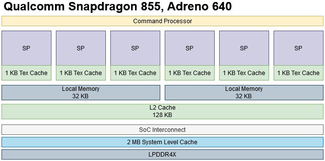
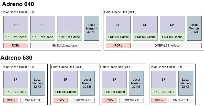
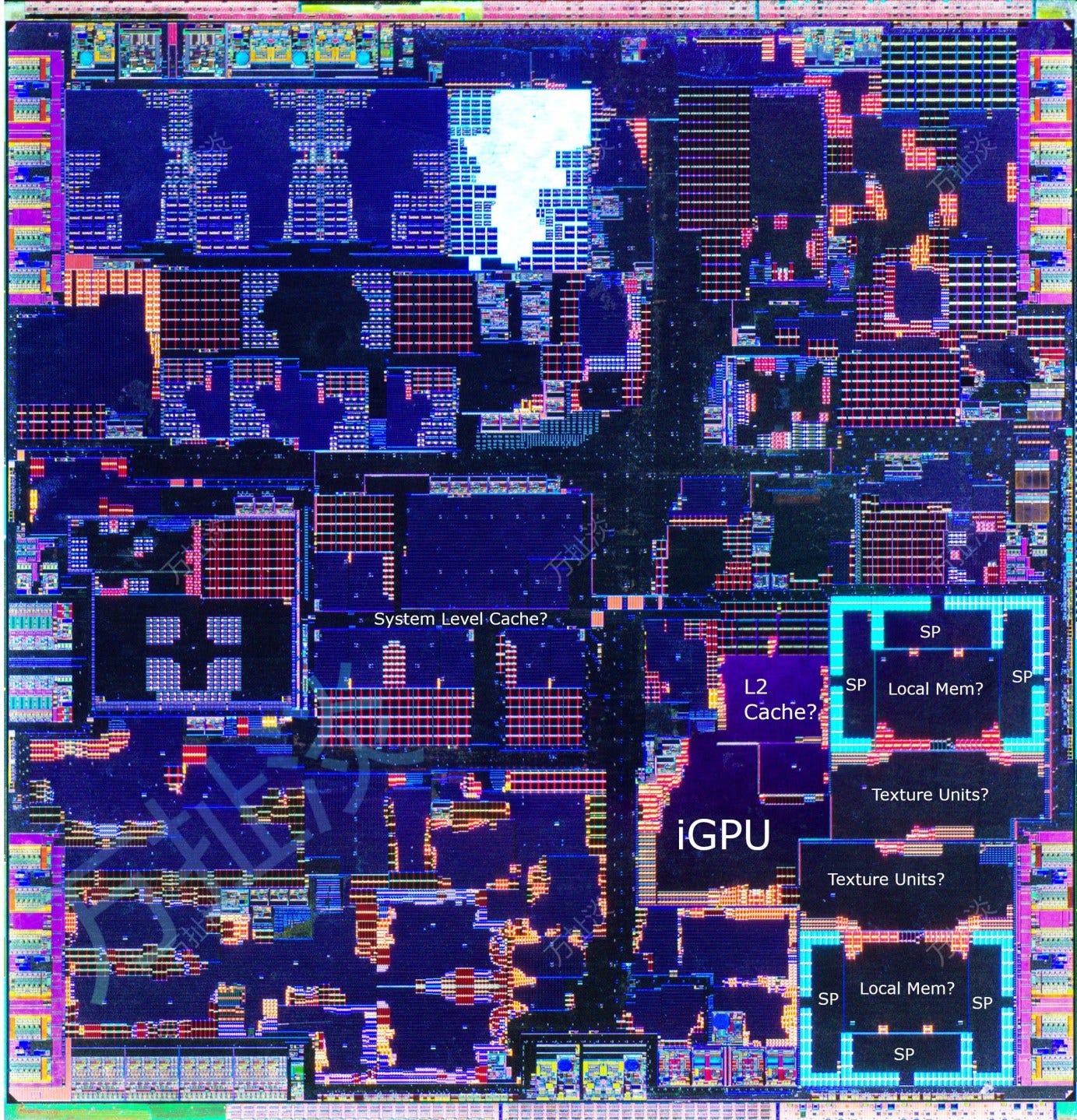
Shader Processors (SPs) are basic compute building blocks for Qualcomm’s iGPUs. Adreno 640 has six of these to Adreno 530’s four, but Qualcomm reorganized the GPU to avoid replicating other hardware resources in a similar manner. SPs are likely organized in groups of three, with local memory and memory interfaces shared across the entire group. Only execution units and texture caches remain private to a SP. Previously, each SP had its own local memory instance.
To further save power and area, Qualcomm reduced GPU clock speeds. That’s remarkable because Adreno 530 already ran at a low 653 MHz. Adreno 640 drops that to just 585 MHz, for a 10.4% clock speed reduction.
Outside the GPU, Adreno 640 benefits from Snapdragon 855’s more modern memory subsystem. A system level cache helps absorb memory requests from blocks across the chip, including the CPU and GPU. Snapdragon 855 further benefits from LPDDR4X, which offers higher bandwidth than the Snapdragon 821’s LPDDR4.
Adreno 640’s Wide Shader Processors
Adreno 640’s SPs also get modifications to cheaply boost compute throughput. GPUs use vector execution, where one instruction applies the same operation across many data elements. Instruction fetch, decode, and scheduling can be expensive, so vector execution saves power and area by making each instruction do more computation work. But those savings mean hardware can’t send a different instruction to a subset of vector lanes. If a branch takes different directions within a vector, GPUs cope by sequentially executing both sides of the branch and deactivating vector lanes to preserve correct behavior. That reduces throughput and can get particularly bad if you’re evil enough to nest diverging branches. GPU (and CPU) designers have to strike a balance between simplifying hardware with wider vectors, and using smaller vectors to reduce divergence losses.
Qualcomm’s engineers struck this balance by dropping a brick onto the “wide vector” side of the scale. Adreno 640 uses vectors that are 128x 32-bit elements wide, or wave128 for short. For comparison, AMD’s GCN architecture uses wave64, while AMD RDNA and Nvidia GPUs use wave32.
Besides using wide vectors, GPUs keep many threads in flight to hide cache and memory latency. Mesa code says Adreno 640 can can track 128 * 4 * 16 fibers per SP. A fiber is a single vector lane and 128 is the wave size, so Mesa code points to four 16 entry schedulers. SP in Mesa code likely maps to what I consider a set of three SPs, because the fibers_per_sp variable is used to manage “private memory”, which probably corresponds to local memory. As we’ll see later, local memory is shared between three SPs.
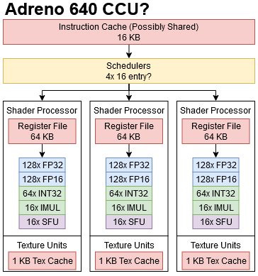
I have no clue how four scheduler partitions would map onto three SPs. I tried to create partition camping issues to infer the partition scheme, but wasn’t successful.
Wave128 also limits how threads can address the register file. Mesa indicates Adreno 640 has 64 KB register files. Assuming each SP can track up to 16 threads, that’s only enough register file capacity for eight wave128 registers per thread. For comparison, AMD’s RDNA2 architecture has 128 KB register files. That’s good for 64 wave32 register per thread, or 32 in wave64 mode. Even if Adreno can keep a lot of threads in flight, eight registers is even less than what CPU vector extensions offer. More complex shaders with lots of live registers might suffer from low occupancy on Adreno.
Execution Units
Once operands are read from the register file, Adreno can start doing real math. Adreno 640 more than doubles compute throughput compared to Adreno 530, and distances itself from Intel’s Skylake iGPU. Each Adreno 640 SP likely has a wide 128-lane FP32 execution unit. FP16 operations execute at approximately the same rate as FP32 ones, breaking from Adreno 530 and 730 where FP16 execute at double rate. Special functions like inverse square roots execute at 1/8 rate. FP64 is not supported.
Integer performance is generally worse compared to AMD, Intel, and Nvidia GPUs. Basic integer adds execute at half rate, and 64-bit precision cuts throughput in half again. On the bright side, Adreno 640 adds hardware INT8 support. Adreno 530 likely didn’t have native INT8 units, and emulated it by masking off higher precision results.
Cache and Memory Access
DRAM performance is completely inadequate for feeding any modern compute device, whether it’s a CPU or GPU. Hardware designers therefore try to service as many memory accesses as possible without going off-chip.
Local Memory
Unlike code running on CPUs, GPU threads typically don’t get bounced between cores. That lets GPUs offer a local memory space backed by core-private SRAM blocks. Local memory is only shared across a group of threads (a workgroup), in contrast to global memory that’s backed by DRAM and shared across the GPU. Software has to explicitly copy data into local memory, unlike caches that transparently handle fills and lookups. Thanks to those restrictions, local memory can be directly addressed. It doesn’t need a cache controller that does tag comparisons for every access. As a result, local memory usually offers guaranteed high bandwidth and low latency. Usually is the key word here.

Adreno 640 lets code allocate up to 32 KB of local memory per workgroup, but can only have 64 KB of local memory active at a time across the GPU. Therefore, it probably has one 32 KB local memory instance per 3 SPs.
Local memory bandwidth barely increases compared to Adreno 530, even though Adreno 640 more than doubles compute throughput.
At least local memory has good latency:
Qualcomm probably decided that sacrificing local memory capacity and bandwidth wouldn’t be a big deal. A lot of shader programs don’t even use local memory because having to explicitly manage data movement presents a huge burden to software. Global memory is much easier to deal with. That’s where caches come in.
Texture Caches
Unlike local memory, caches have extra logic and storage to map their smaller capacity to a subset of global memory. Adreno 640’s first level caches are read-only, non-coherent texture caches. Each SP has one, and each texture cache only has 1 KB of capacity like every other Adreno GPU I’ve seen.
Texture cache bandwidth across the GPU is pretty good because each SP has its own texture cache instance, unlike with local memory. Adreno 640 doesn’t quite keep the same bandwidth to texture cache compute ratio as Adreno 530, but offers a huge jump in absolute terms.
Adreno 640 has slightly higher texture cache latency than Adreno 530.
L2 Cache and Beyond
Adreno’s texture cache is very limited thanks to its small size and lack of write support. The GPU’s L2 cache is the first stop for compute accesses. Adreno 640 has a 128 KB L2 cache, just like Adreno 530. Latency is slightly higher, but that’s down to Adreno 640’s clock speed regression. Both GPUs take about 47 cycles to get data from L2.
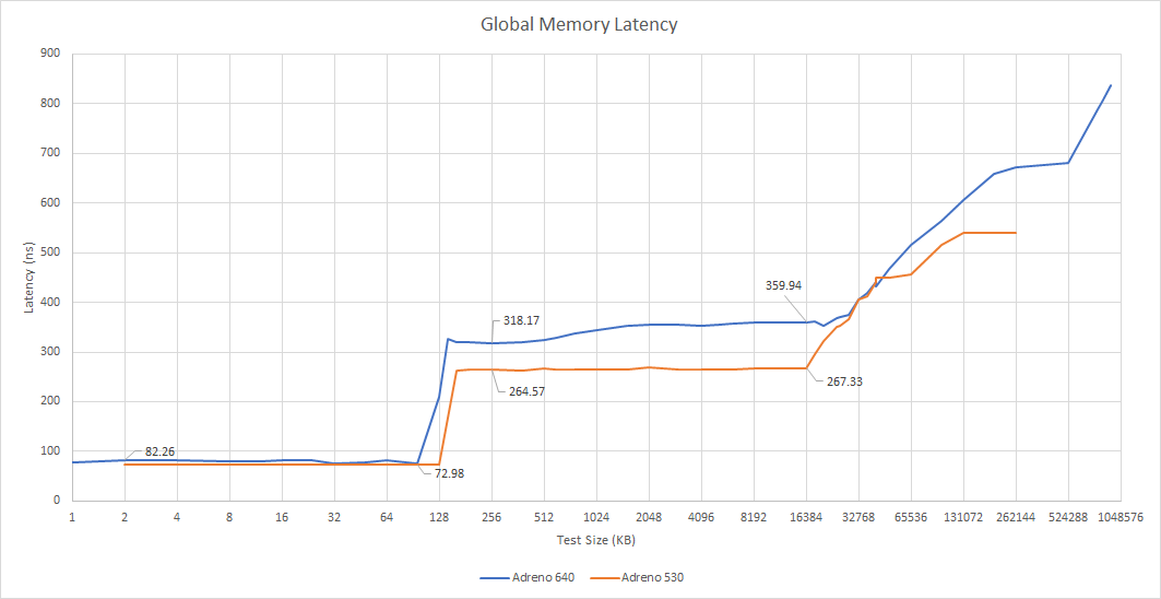
L2 misses go across the on-chip interconnect. On Snapdragon 821, that leads straight to the memory controllers. Snapdragon 855 has a system level cache and sees less latency for test sizes between 128 KB and 2 MB. However, Snapdragon 821 can access main memory with even less latency than that. Both Adreno GPUs see memory latency skyrocket at larger test sizes, likely from TLB misses.
L2 bandwidth is approximately doubled from Adreno 530, and is very close to local memory bandwidth. Usually a shared L2 cache has far less bandwidth than local memory, but not on Adreno 640.
Snapdragon 855’s system level cache offers about 40 GB/s, while main memory bandwidth is a touch below 30 GB/s.
Compute Performance: FluidX3D
FluidX3D simulates fluid behavior. Qualcomm GPUs do very poorly in this workload, and Snapdragon 855 somehow manages to regress compared to Snapdragon 821.
With FluidX3D, Adreno 640 does a very good job of turning the phone into a hand warmer without getting much done.
Rasterization: 3DMark
Adreno GPUs are built for tiled rendering, which optimizes the traditional rasterization pipeline. Geometry gets sorted into tiles, which are then rendered one at a time. Tiles are kept in specialized on-chip storage (GMEM) while they’re being rendered, saving memory bandwidth. Linux driver code indicates that Adreno 640 and 530 both have a 1 MB of GMEM, while Adreno 730 has a 2 MB of GMEM. I’ll be comparing to the Snapdragon 8+ Gen 1’s Adreno 730 here because Snapdragon Profiler couldn’t show GPU metrics for the Snapdragon 821.
3DMark is a popular GPU benchmark suite. Here I’m using Snapdragon Profiler to get data on 3DMark’s Slingshot Extreme and Wild Life Extreme tests. I ran both tests in unlimited mode to factor out screen resolution. In Slingshot Extreme, Adreno 640’s shaders are busy around 90% of the time, while ALU capacity sees 30-40% utilization. Adreno 730 is enjoys better ALU utilization at 50-60%. Texture pipes are quite busy on both GPUs, though Adreno 730 again has an easier time keeping itself fed.
3DMark’s Wild Life Extreme benchmark is more demanding. The Snapdragon 8+ Gen 1’s Adreno 730 can only average 16 FPS, while Adreno 640 in the Snapdragon 855 only runs at 5.2 FPS. Adreno 640 has a harder time keeping its ALUs fed, with utilization staying around 30%. Adreno 730 does better, but no longer enjoys the good 50% utilization it did in Slingshot Extreme.
Good caching is vital to maintaining high performance. Adreno 640’s 1 KB texture caches enjoy a surprisingly good 68.1% average hitrate, while the 128 KB L2 catches over 90% of L1 misses. Adreno 730 has a somewhat lower 65.5% L1 texture cache hitrate, but its larger 256 KB L2 brings hitrate at that level to 95.8%.
Wild Life Extreme shows a similar pattern, except Adreno 730’s 256 KB L2 barely sees any misses. Snapdragon 855’s Adreno 640’s smaller L2 still does fine. Tiled rendering probably helps reduce the texture footprint for each tile, letting Adreno’s relatively small caches do a good job.
Cache misses consume memory bandwidth, which can be a scarce commodity on mobile chips. Snapdragon Profiler provides GPU memory read and write bandwidth metrics. I’m not sure if that’s measured before or after the system level cache.
Adreno 640 consumes modest amounts of bandwidth on Slingshot Extreme, so caches (and GMEM) are doing their job. GPU memory read/write bandwidth rarely exceeds 10 GB/s. Adreno 730 sees around twice as much bandwidth usage. Even though its caches also do a good job, the newer GPU’s larger shader array demands more data. Curiously, Adreno 730 has a higher write percentage too.
Wild Life Extreme sees broadly similar read-to-write ratios. Again caches keep memory bandwidth demands under control. The Snapdragon 855 stayed below 10 GB/s most of the time, while the Snapdragon 8+ Gen 1 mostly stayed below 20 GB/s. Both chips have plenty of memory bandwidth to spare, even though they use narrow 64-bit DRAM buses.
Even though framerate was a tad low, Adreno 640 did a good job of maintaining low temperatures without dropping clocks. Clock speed remained at 585 MHz, while temperatures stayed below 70 C. The OnePlus 7 Pro doesn’t have active cooling, so Qualcomm did an excellent job of designing a low power GPU.
Final Words
Adreno 640 isn’t a straightforward evolution of the older Adreno 530. Instead, Qualcomm’s engineers went through a pile of tricks to maximize compute throughput without blowing power and area budgets. Extremely wide vector width and resource sharing between SPs let Qualcomm spend more transistors on execution units and less on supporting logic. That extends to the cache hierarchy, where Adreno 640 sticks to 1 KB texture caches and a 128 KB shared L2 cache. It’s a great demonstration of how to make GFLOPS go up on a shoestring silicon budget.
Qualcomm combines improved compute throughput with tiled based rendering, letting Adreno do well with rasterized graphics. Tiling keeps memory bandwidth demands under control, an impressive feat on cell phone SoCs with 64-bit LPDDR buses. Compute doesn’t receive the same attention. The L1 texture caches are tiny and can’t support writes, while the L2 cache’s 128 KB capacity is mediocre at best. Memory latency is staggeringly high past 64 MB. Even though the GPU can access up to 3.65 GB of memory, single allocations are limited to under 1 GB. That can be limiting for compute workloads that work on a large grid uploaded to the GPU as a single allocation.
Exiting the process GpuMemLatency_aarch64 from function cl_a6x_cmdbuf_mgr_submit_ibs and line 1068
What happens if a kernel runs too long
I also had difficulty microbenchmarking the GPU through OpenCL. Qualcomm’s OpenCL runtime would unpredictably crash if a kernel ran for too long. Crash probability goes down if kernel runtimes stay well below a second. That’s why some of the graphs above are noisy. I wonder if Qualcomm’s Adreno 6xx command processor changes had something to do with it. They added a low priority compute queue, but I’m guessing OpenCL stuff doesn’t run as “low priority” because the screen will freeze if a kernel does manage to run for a while.
Qualcomm’s newer Adreno 730 reverts some of Adreno 640’s changes. Divergence penalties went down, suggesting a move back to wave64 vectors. Local memory became SP-private again. Still, Adreno 640 is a showcase of how Qualcomm is willing to try different things.
Finally, special thanks goes to Zarif98 for providing the OnePlus 7 Pro for testing.
If you like our articles and journalism, and you want to support us in our endeavors, then consider heading over to our Patreon or our PayPal if you want to toss a few bucks our way. If you would like to talk with the Chips and Cheese staff and the people behind the scenes, then consider joining our Discord.


