
Inside SiFive’s P550 Microarchitecture

RISC-V is a relatively young and open source instruction set. So far, it has gained traction in microcontrollers and academic applications. For example, Nvidia replaced the Falcon microcontrollers found in their GPUs with RISC-V based ones. Numerous university projects have used RISC-V as well, like Berkeley’s BOOM. However, moving RISC-V into more consumer-visible, higher performance applications will be an arduous process. SiFive plays a key role in pushing RISC-V CPUs toward higher performance targets, and occupies a position analogous to that of Arm (the company). Arm and SiFive both design and license out IP blocks. The task of creating a complete chip is left to implementers.
By designing CPU blocks, both SiFive and Arm can lower the cost of entry to building higher performance designs in their respective ISA ecosystems. To make that happen within the RISC-V ecosystem though, SiFive needs to develop strong CPU cores. Here, I’ll take a look at SiFive’s P550. This core aims for “30% higher performance in less than half the area of a comparable Arm Cortex A75.”
Just as with Arm’s cores, P550’s performance will depend heavily on how it’s implemented. For this article, I’m testing the P550 as implemented in the Eswin EC7700X SoC. This SoC has a 1.4 GHz, quad core P550 cluster with 4 MB of shared cache. The EIC7700X is manufactured on TSMC’s 12nm FFC process. The SiFive Premier P550 Dev Board that hosts the SoC has 16 GB of LPDDR5-6400 memory. For context, I’ve gathered some comparison data from the Qualcomm Snapdragon 670 in a Pixel 3a. The Snapdragon 670 has a dual core Arm Cortex A75 cluster running at 2 GHz.
Overview
The P550 is a 3-wide out-of-order core with a 13 stage pipeline. Out-of-order execution lets the core move past a stalled instruction to extract instruction level parallelism. It’s critical for achieving high performance because cache and memory latency can be significant limiters for modern CPUs. The P550 is far from SiFive’s first out-of-order design. That distinction belongs to SiFive’s U87, which is also a 3-wide out-of-order design. P550 comes several years after, and should be more mature.

Arm’s Cortex A75 is also a 3-wide out-of-order core. It’s an improved version of Arm’s Cortex A73, and carries forward distinguishing features like out-of-order retirement. Anandtech says A75 has a 11-13 stage pipeline, though their diagram suggests the minimum mispredict penalty is likely closer to 11 cycles.
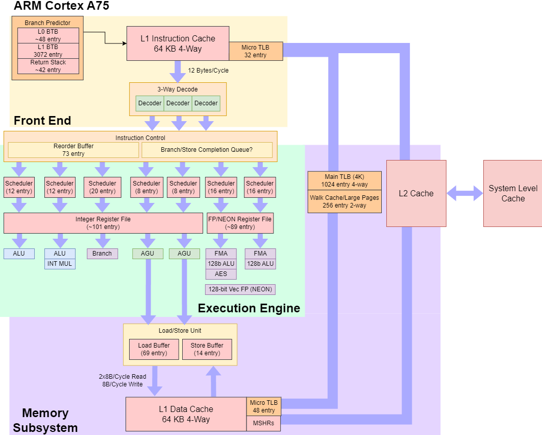
Like SiFive’s P550, the Arm Cortex A75 has a modestly sized out-of-order execution engine. Both are far off the high performance designs we see from Intel and AMD today, and are optimized for low power and area.
Branch Prediction
Fast and accurate branch prediction is critical to both performance and power efficiency. SiFive has given the P550 a 9.1 KiB branch history table, which helps the core correlate past branch behavior with branch outcomes. From an abstract test with various numbers of branches that are taken/not-taken in increasingly long random patterns, the P550’s branch predictor looks to have reasonably good pattern recognition capabilities. It falls well short of high performance cores, but that’s to be expected.
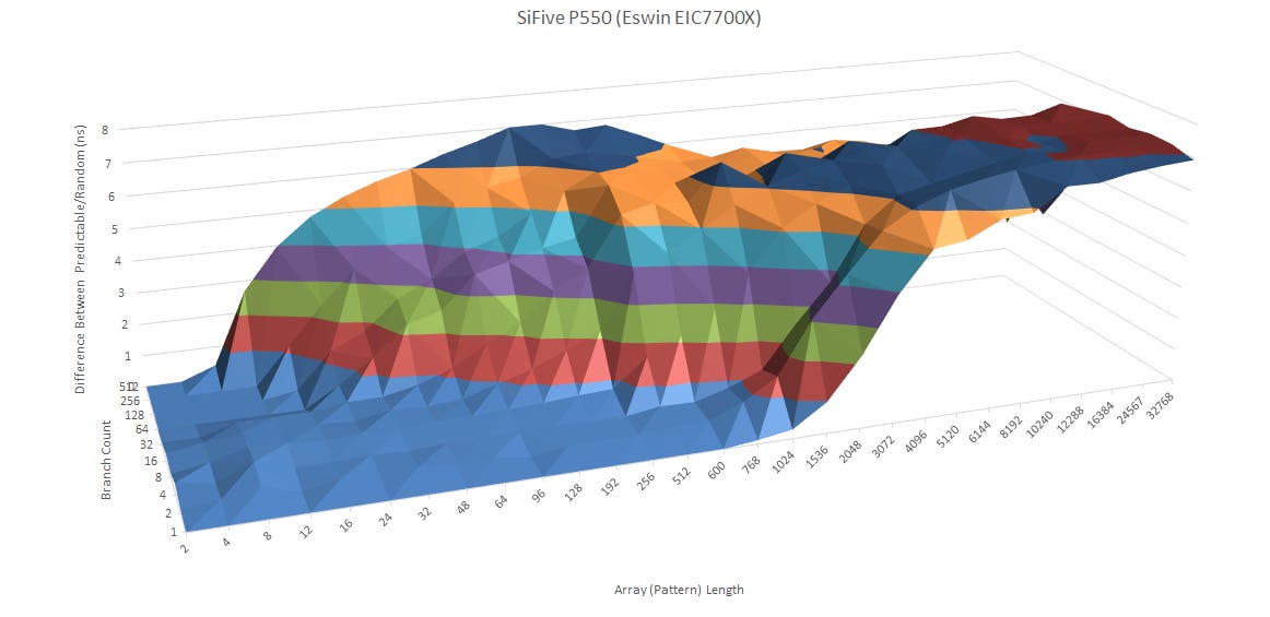
Compared to Arm’s Cortex A75, the P550 can handle longer patterns for a small number of branches. The gap however narrows as more branches come into play.

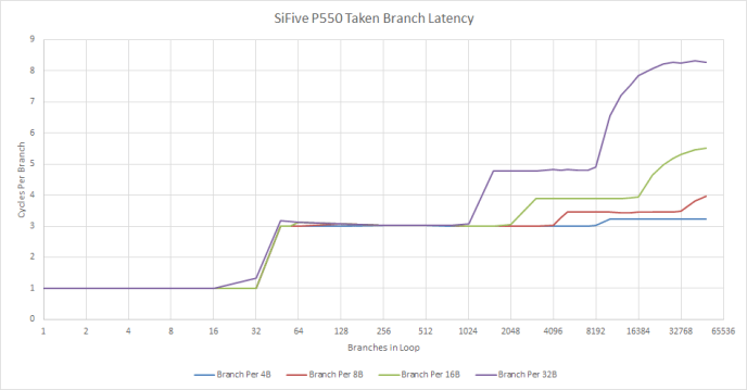
Branch predictor speed can matter too, especially in high IPC code with a lot of branches. The P550 appears to have a 32 entry BTB capable handling taken branches with no bubbles. Past that, the core can handle a taken branch every three cycles as long as the test fits within 32 KB. Likely, P550 doesn’t have another BTB level. If a branch misses the 32 entry BTB, the core simply calculates the branch’s destination address when it arrives at the frontend. If so, the P550’s 32 KB L1 instruction cache has 3 cycles of latency.
Arm’s Cortex A75 also uses what appears to be a single small BTB level. Both cores lack the large decoupled BTBs that high performance cores tend to have.

P550 uses a 16 entry return stack to predict returns from function calls. A75 seems to have a return stack with 42 entries, because latency per call+return pair doesn’t hit an inflection point until I get past that. Even with the larger return stack, A75’s higher 2 GHz clock speed lets it achieve similar performance for the common case of a return stack hit.
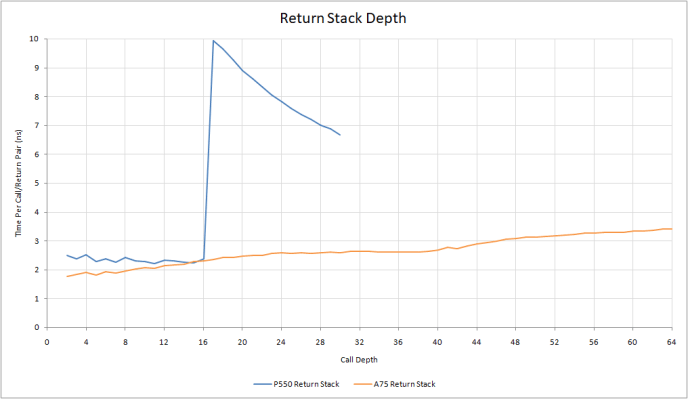
When return stack capacity is exceeded, P550 sees a sharp spike in latency. That contrasts with A75’s more gentle increase in latency. Perhaps A75 only mispredicts for the return address that got pushed out of the stack. P550 possibly has less graceful handling for return stack overflows, making it mispredict many of the returns even when the test only exceeds return stack capacity by a few entries.
Fetch and Decode
The P550’s frontend comes with a parity protected 32 KB 4-way set associative instruction cache, capable of delivering enough bandwidth (12 bytes/cycle) to feed the 3-wide decoder downstream. The frontend can sustain 3 IPC as long as code fits within L1i. Instruction bandwidth takes a gradual drop past that. From L2, the core can still maintain a reasonable 2 IPC. Instruction bandwidth from L3 is good for 1 IPC, though you’d really hope L2 code misses are rare on any core.

Arm chose to give A75 a larger 64 KB instruction cache, giving it a better chance of satisfying instruction-side memory accesses from L1i. On a L1i miss, instruction bandwidth takes a sharp decline. Much of that is down to implementation decisions. Qualcomm gave the Snapdragon 670 a 1 MB system level cache. System level caches are placed closer to the memory controller than compute blocks. Therefore, they usually aren’t optimized to provide high performance for any one block. In contrast, the 4 MB L3 on the EIC7700X is tightly tied to the CPU cluster.
Fetched instructions are decoded into micro-ops, which pass through the renamer and head to the out-of-order backend.
Out-of-Order Execution
SiFive’s P550 has somewhat higher reordering capacity than Arm’s Cortex A75. However, Arm can make its out-of-order execution buffers go a bit further thanks to the out-of-order retirement trick carried forward from A73. On A75, I’m using an incomplete branch along with an incomplete load to block retirement.

Both cores have plenty of register file capacity compared their ROB size, though other structures like memory ordering queues can be a bit thin. P550 and A75 have nowhere near as much reordering capacity as current Intel and AMD cores, or even more recent Arm cores like the Cortex A710. They’re more comparable to Intel’s Core 2 or Goldmont Plus. Still, a modest out-of-order execution window is far better than in-order execution.
Execution resources on both cores are both allocated with low power and low area goals in mind. Between the two, P550 has a more flexible integer port setup and more scheduling capacity to feed those ports. Cortex A75 isn’t far behind though, with two ALU ports and a separate branch port. Scalar integer workloads often have a lot of branches, and a branch port doesn’t need a writeback path to the register file. Arm’s setup is likely a cheaper, while providing almost as much performance.
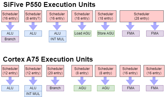
On the floating point side, both cores have two FP ports capable of handling the most common operations. P550 handles FP adds, multiplies, and fused multiply-adds (FMAs) with 4 cycle latency, suggesting the core uses FMA units to handle all of those operations. After all, an add is simply a FMA with a multiplier of 1, and a multiply is a FMA with the addend equal to 0. A75 has 3 cycle latency for FP adds and multiplies, while FMAs execute over 5 cycles. Arm may use separate execution units for FMAs and adds/multiplies. Or, Arm might have a FMA unit with optimized paths for doing just multiplies or just adds. Cortex A75’s FPU also supports vector execution, giving it a leg up over P550.
Microbenchmarking suggests A75 has 31 scheduler entries available for floating point operations. Anandtech says A75 has two 8-entry floating point schedulers, but my measurements disagree. P550 has 28 total scheduler entries for FP operations. This could be a dual ported unified scheduler, or two 14 entry schedulers. I haven’t found an operation that only goes to one port.
Memory Subsystem
P550 is a small, low power design and doesn’t need the high throughput memory subsystems found on Intel, AMD, or Arm’s big cores. Memory operations first have their addresses generated by two address generation units (AGUs). One handles loads, and the other handles stores. Both appear to be backed by relatively large schedulers, letting the core handle workloads with an uneven balance of loads and stores. Cortex A75 also has two AGUs, but each of A75’s AGU pipes can handle both loads and stores. Two load/store ports make a lot of sense because loads usually greatly outnumber stores, so P550’s load AGU may be very busy while the store AGU is mostly idle.
…we observed that each of the two load/store ports were used about 20 percent of the time. We surmised that changing to one dedicated load port and one dedicated store port should not have a large effect on performance…This proved to be the case, with less than a 1 percent performance loss for this change.
David B. Papworth, Tuning the Pentium Pro Microarchitecture
Curiously, Intel evaluated the same tradeoff when they designed their Pentium Pro back in 1996. They found using a less flexible load/store setup only came with a minor performance impact. SiFive may have come to the same conclusion. P550 does have more reordering capacity than the Pentium Pro though, and thus would be better able to feed its execution pipes (including the AGUs) in the face of cache misses.

AGUs generate program-visible virtual addresses, which have to be translated to physical addresses. P550 uses a two-level TLB setup to speed up address translation. The first level TLBs are fully associative, meaning that any entry can cache a translation for any address. However, both the data and instruction side TLBs are relatively small with only 32 entries. A larger 512 entry L2 TLB serves both instruction and data L1 TLB misses. On the data side, getting a translation from the L2 TLB adds 9 cycles of latency. Arm’s A75 has larger TLBs, and a lower 5-6 cycle penalty for hitting the L2 TLB.
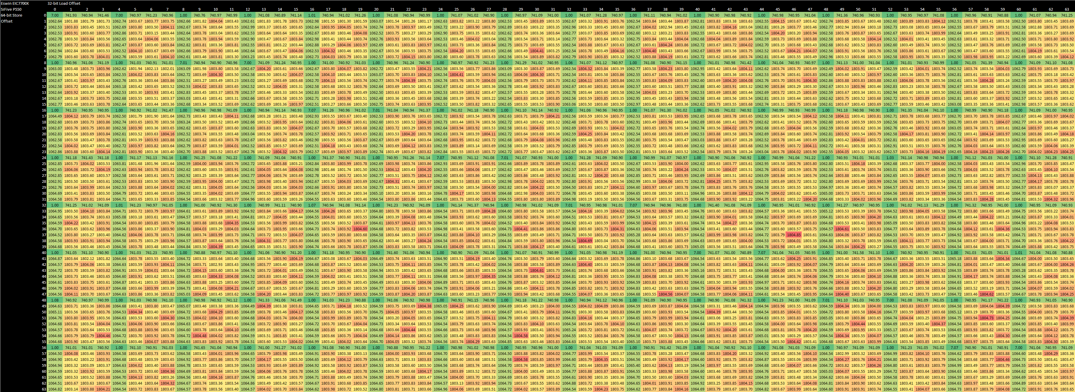
Before accessing cache, load addresses have to be checked against older stores (and vice versa) to ensure proper ordering. If there is a dependency, P550 can only do fast store forwarding if the load and store addresses match exactly and both accesses are naturally aligned. Any unaligned access, dependent or not, confuses P550 for hundreds of cycles. Worse, the unaligned loads and stores don’t proceed in parallel. An unaligned load takes 1062 cycles, an unaligned store takes 741 cycles, and the two together take over 1800 cycles.
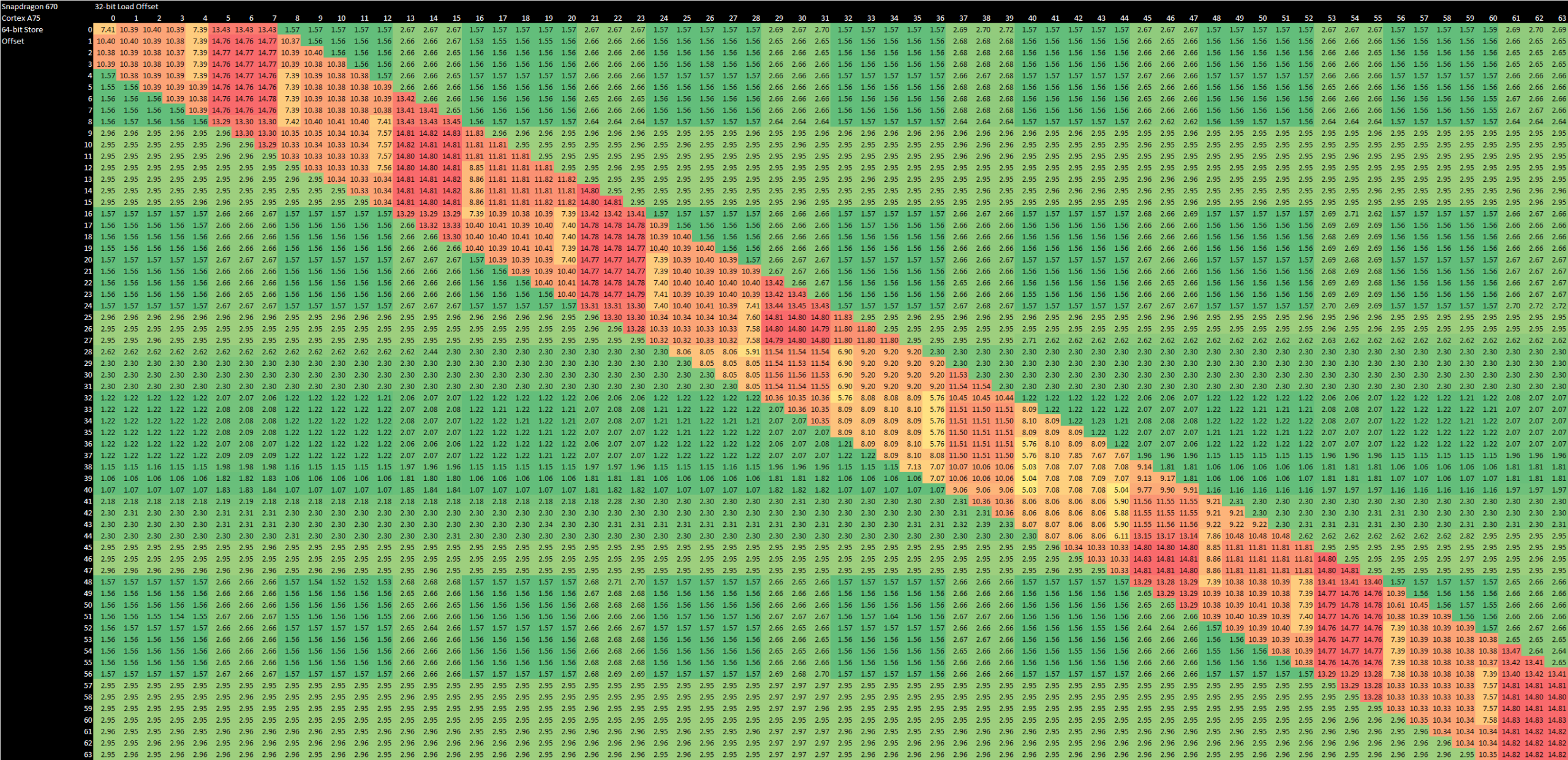
This terrible unaligned access behavior is atypical even for low power cores. Arm’s Cortex A75 only takes 15 cycles in the worst case of dependent accesses that are both misaligned.
Digging deeper with performance counters reveals executing each unaligned load instruction results in ~505 executed instructions. P550 almost certainly doesn’t have hardware support for unaligned accesses. Rather, it’s likely raising a fault and letting an operating system handler emulate it in software.
Core-Private Caches
With a modest out-of-order execution engine and no vector capability, P550 doesn’t demand a lot of bandwidth from it’s memory subsystem. Latency however is very important, because P550 doesn’t have the massive reordering capacity that higher performance cores use to tolerate memory latency. Like many AMD, Intel, and Arm designs, each P550 core has its own L1 and L2 caches while L3 is shared. All levels of the data-side cache hierarchy are ECC protected.
P550’s 32 KB L1 data cache is 4-way set associative, and can service a load and a store every cycle, assuming no alignment issues. Maximum bandwidth is thus 16 bytes per cycle, achieved with an even mix of reads and writes. Latency is 3 cycles, matching many low-clocked cores.
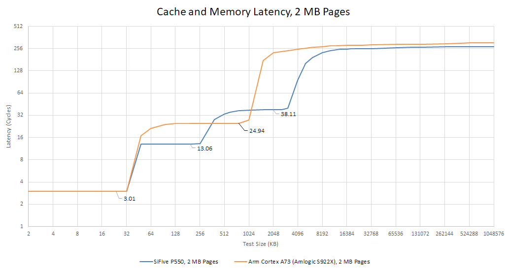
The L2 cache is 256 KB and 8-way set associative. It’s built from two banks, and has 13 cycle latency. This combination of size and latency is a bit dated, as Arm and AMD have both implemented larger L2 caches with lower latency. However, P550’s L2 is still well positioned to catch L1 misses and insulate the core from L3 latency. L2 bandwidth is mediocre at 8 bytes per cycle, a limitation that applies to both reads and writes. While it’s not an impressive figure, 8 bytes per cycle should be adequate considering the core’s lack of vector capability and single load AGU.

Arm’s Cortex A75 enjoys higher cache bandwidth, thanks both to higher clock speeds and more per-cycle bandwidth at each level.
L3 Cache and Interconnect
P550’s interconnect has to be modular and scalable to address the largest possible market. A consumer router or set-top box may be fine with 2-4 cores, while a small edge server might benefit from higher core counts. P550 can be instantiated in clusters of up to four cores. Presumably, cores within a cluster share a single external interface. Multiple clusters sit on a “Coherent System Fabric”, which sends traffic coming off P550 clusters to the appropriate destination. From the EIC7700X datasheet, this “Coherent System Fabric” is likely a crossbar.
Cacheable memory accesses head to a L3 cache, which can be shared across multiple P550 clusters and is banked to meet the bandwidth demands of multiple cores. SiFive provides 1 MB, 2 MB, 4 MB, and 8 MB L3 capacity options. The largest 8 MB option has eight banks and is reserved for multi-cluster configurations. The EIC7700X we’re looking at has a 4 MB L3 with four banks. Bank count thus matches core count.

Microbenchmarking indicates the L3 can give 8 bytes per cycle of bandwidth to each core. In total, the EIC7700X’s quad core P550 cluster has about 43.88 GB/s of L3 bandwidth. L3 latency is respectable at about 38 cycles, which isn’t bad considering the cache’s flexibility. For comparison, Arm’s Cortex A73 uses a simpler two-level cache setup. A73’s L2 serves double duty as the first stop for L1D misses and as a large last level cache. That means compromise, so the 1 MB L2 has less capacity than EIC7700X’s L3 while having better latency at 25 cycles.

L3 misses head out to a Memory Port. Depending on implementation goals, a P550 multi-cluster complex can have one or two memory ports, each of which can be 128 or 256 bits wide. Each Memory Port can track up to 128 pending requests to enable memory level parallelism. Less common requests to IO or non-cacheable addresses get routed to one of two 64-bit System Ports or a 64-bit Peripheral Port. Implementers can also use one or two Front Ports, which gives other agents coherent memory access through the multi-cluster complex.

Eswin has chosen to use a single Memory Port, likely 128 bits wide, and two System Ports. The first System Port’s address space includes a 256 MB PCIe BAR space, PCIe configuration space, and 4 MB of ROM. The second System Port accesses the DSP’s SRAM, among other things.
Those ports connect to the on-chip network, which uses the AXI protocol. At this point, everything is up to the implementer and is out of SiFive’s hands. For the EIC7700X, Eswin used two DDR controllers, each with two 16-bit sub-channels. On the SiFive Premier P550 Dev Board, they’re connected to 16 GB of LPDDR5-6400. The memory controller runs at 1/4 of the SDRAM clock, which would be 800 MHz. DRAM load-to-use latency isn’t great at 194 ns, which is about 165 ns beyond L3 latency. It’s impossible to tell how much of this latency comes from traversing the on-chip network versus the memory controller. But either way, memory latency on the EIC7700X is substantially worse than other LPDDR5 setups like Intel’s Meteor Lake or AMD’s Van Gogh (Steam Deck SoC).

I measured 16.74 GB/s of DRAM bandwidth, which is well short of what LPDDR5-6400 should be capable of even with a 64-bit bus. The EIC7700X uses some bus width for inline ECC, but achieved bandwidth is well short of theoretical even with that in mind. Still, that sort of bandwidth should be adequate for a very low clocked quad core setup with no vector capability.
Core to Core Latency
Rarely, the interconnect may need to carry out cross-core transfers to maintain cache coherency. Eswin’s EIC7700X datasheet says the memory subsystem has a “directory based coherency manager”, meaning memory accesses check the directory to see whether they need to send a probe or can proceed as normal down the memory hierarchy. Compared to a broadcast strategy, using a directory keeps probe traffic under control as core counts go up.
Anandtech and other sites have used “core to core” latency tests to check how long it takes for a core to observe a write from another, and I’ve written my own version of the test. Although the exact methodology differs, results should be broadly comparable to those from Anandtech. Core to core latency on the EIC7700X is quite high.

Qualcomm’s Snapdragon 670 does much better, even when transfers happen between A75 and A55 cores.
While high core to core latency is unlikely to impact application performance, it does contribute to the feeling that SiFive’s P550 isn’t quite so polished.
Final Words
RISC-V is a young instruction set and SiFive is a new player in the CPU design business. High performance CPU design is incredibly challenging, as shown by the small number of players in that space. P550 aims for “the highest performance within a tightly constrained power and area footprint” according to the company’s datasheet. It doesn’t go head-on against the likes of AMD’s Zen 5, Intel’s Lion Cove, or Qualcomm’s Oryon. P550’s out-of-order engine is closer in size to something like Intel’s Core 2 from over 15 years ago. Combine that with much lower clock speeds than even what Core 2 ran at, and P550 is really a low power core with modest performance. It’s best for light management tasks where an in-order core may be a tad sluggish.

More importantly, P550 represents a stepping stone in SiFive’s journey to push RISC-V to higher performance targets. Not long ago, SiFive primarily focused tiny in-order cores not suitable for much more than microcontrollers. With the P550, SiFive has built a reasonably well balanced out-of-order engine supported by a competent cache hierarchy. They got the basics down, and I can’t emphasize how important that is. Out-of-order execution has proven essential for building high performance, general purpose CPUs, but is also difficult to pull off. In fact, both Intel and IBM tried to step away from out-of-order execution because it added so much complexity, only to find out Itanium and POWER6’s strategies weren’t great. With that in mind, SiFive’s progress is promising.
Still, the P550 is just one step in SiFive’s journey to create higher performance RISC-V cores. As a step along that journey, P550 feels more comparable to one of Arm’s early out-of-order designs like Cortex A57. By the time A75 came out, Arm already accumulated substantial experience in designing out-of-order CPUs. Therefore, A75 is a well polished and well rounded core, aside from obvious sacrifices required for its low power and thermal budgets. P550 by comparison is rough around the edges. Its clock speed is low. Misaligned access penalties are ridiculous. Vector support is absent. Many programs won’t hit the worst of P550’s deficiencies, but SiFive has a long way to go.
In that respect, I can also see parallels between P550 and Intel’s first out-of-order CPU. The Pentium Pro back in the mid 1990s performed poorly when running 16-bit code. But despite its lack of polish in certain important areas, the core as a whole was well designed and gave Intel confidence in tackling more complex CPU designs. SiFive has since announced more sophisticated out-of-order designs like the P870. I’ll be excited to see those cores implemented in upcoming chips, because they look quite promising.
If you like the content then consider heading over to the Patreon or PayPal if you want to toss a few bucks to Chips and Cheese. Also consider joining the Discord.
It would be interesting to run tests on Tenstorrent's silicon
Expensive, slow and incompatible. A long way to go before it becomes something meaningful for consumers.
I assume there's no way to run SPEC on this?