
Huawei's Kunpeng 920 and TaiShan v110 CPU Architecture
Investigating Huawei's unique L3 design and their first in-house core

Huawei is one of China’s largest technology companies, with enterprise products spanning everything from servers to networking equipment. All of those products require advanced chips to remain relevant. Huawei has invested in developing its own chips with its HiSilicon subsidiary, which lets Huawei both tailor chip designs to its requirements and safeguard its business against supply chain disruptions. Kunpeng 920 is a chiplet-based CPU design that targets a variety of enterprise applications including cloud servers, AI accelerators, and wireless base stations.
Here, we’re looking at a 24 core Kunpeng 920 CPU subsystem found in a Huawei network card.
Special thanks goes out to Brutus for setting this one up!
System Architecture
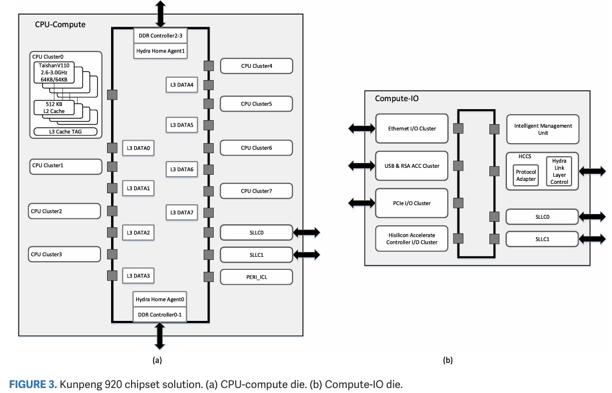
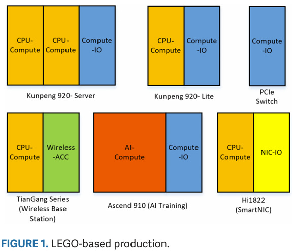
Kunpeng 920 uses multiple dies with TSMC’s CoWoS packaging to implement what HiSilicon calls “LEGO-based production”. HiSilicon’s chiplet strategy uses dies of equal height placed side-by-side, with compute dies in the center and IO dies on the side. Compute dies are called Super CPU Clusters (SCCLs) and include DDR4 controllers on the top and bottom edges of the die, which uses all of the chip’s edge area for off-chip interfaces. The SCCLs are fabricated on TSMC’s 7nm process and contain up to 32 TaiShan v110 CPU cores with L3 cache. A separate IO die uses TSMC’s 16nm node, and connects to PCIe, SATA, and other lower speed IO. All dies sit on top of a 65nm interposer.
Inter die bandwidth is able to achieve up to 400 GB/s with coherency
Kunpeng 920: The First 7-nm Chiplet-Based 64-Core ARM SoC for Cloud Services
HiSilicon’s LEGO-based production has parallels to Intel’s chiplet strategy, which similarly emphasizes high cross-die bandwidth at the cost of more expensive packaging technologies and tighter distance limits between dies. Like Intel’s Sapphire Rapids, placing memory controllers at the CPU dies lets smaller SKUs access DRAM without needing to route memory requests through another chiplet. Sapphire Rapids uses its high cross-die bandwidth to make its multi-die setup appear monolithic to software. L3 and DRAM resources can be seamlessly shared across dies, in contrast to a NUMA setup where software has to work with different memory pools.Strangely, I wasn’t able to find any evidence that Kunpeng 920 could combine L3 and DRAM resources across multiple SCCLs.
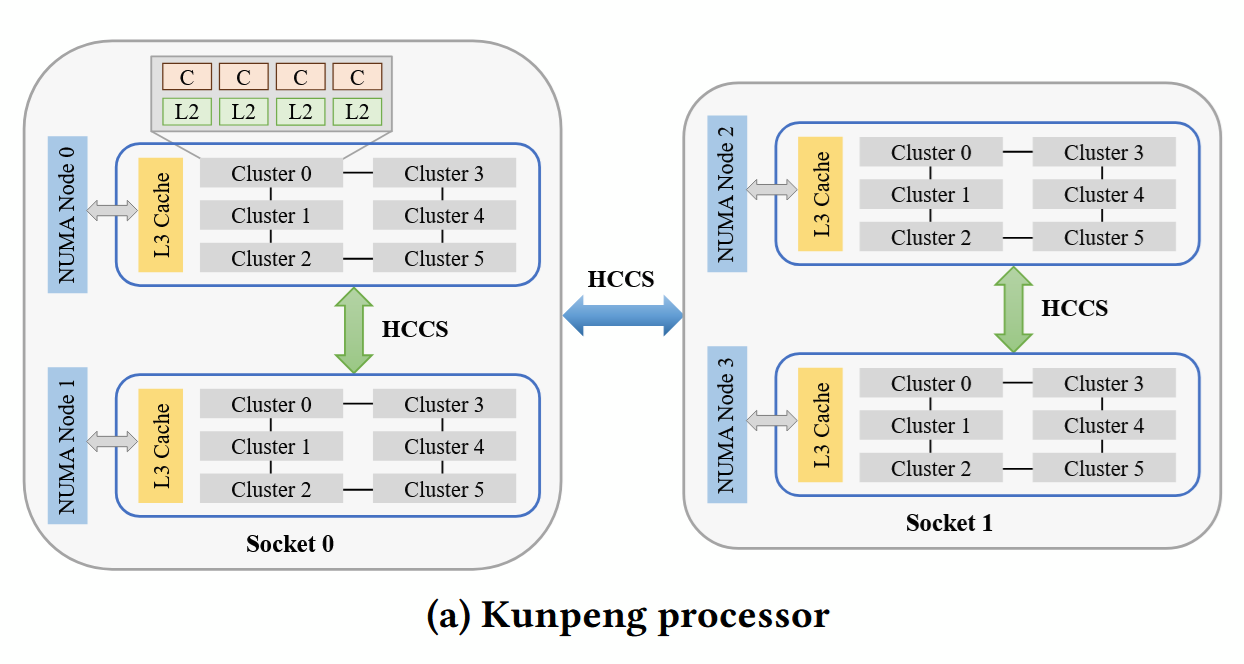
Kunpeng 920 supports dual and quad socket configurations using Huawei’s “Hydra” links, which helps scale core counts further. Contemporary server processors with similar per-socket core counts, like Ampere Altra and AMD’s Zen 2, only scale up to dual socket configurations.
Compute Die Topology and L3 Cache
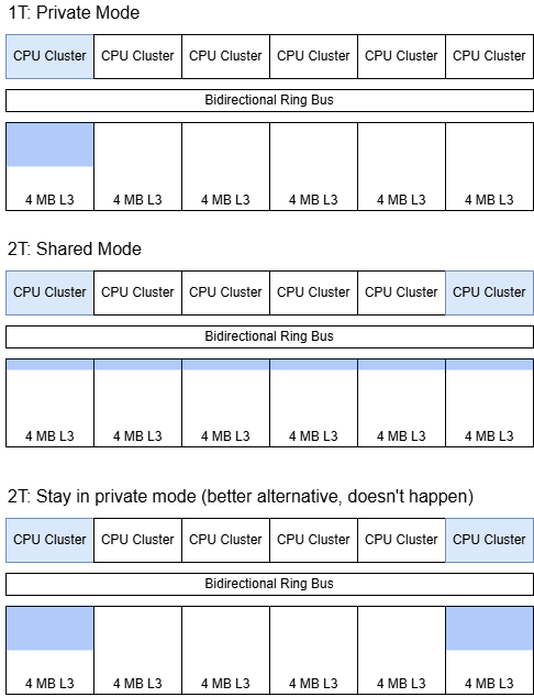
TaiShan v110 cores within a SCCL compute die are grouped into quad core CPU clusters (CCLs). A bidirectional ring bus links blocks on the compute die, including CPU clusters, L3 data banks, memory controllers, and links to other dies. L3 data banks are paired with CPU clusters, but appear to sit on separate ring stops instead of sharing one with a CPU cluster as they do on Intel and AMD designs. A fully enabled SCCL with eight CPU clusters has 21 ring stops. Our 24 core SKU likely has two CPU clusters and L3 banks disabled, though it’s not clear whether the ring stops remain active
Unusually, Huawei places L3 tags at the CPU clusters rather than at the L3 data banks. The L3 can also operate in different modes. “Shared” mode behaves like the L3 on AMD, Arm, and Intel chips, using all L3 banks together to form a large shared cache. Presumably the physical address space is hashed across L3 banks, evenly distributing accesses across the data banks to scale bandwidth while preventing data duplication. “Private” mode makes a L3 bank private to the closest CPU cluster, improving L3 performance by taking much of the interconnect out of the picture. A third “partition” mode can adjust each core cluster’s private L3 capacity on the fly. Huawei’s paper implies partition mode can also dynamically adjust L3 policy between shared and private mode, handling situations where different tasks or even phases of the same task prefer private or shared L3 behavior.
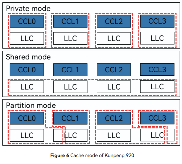
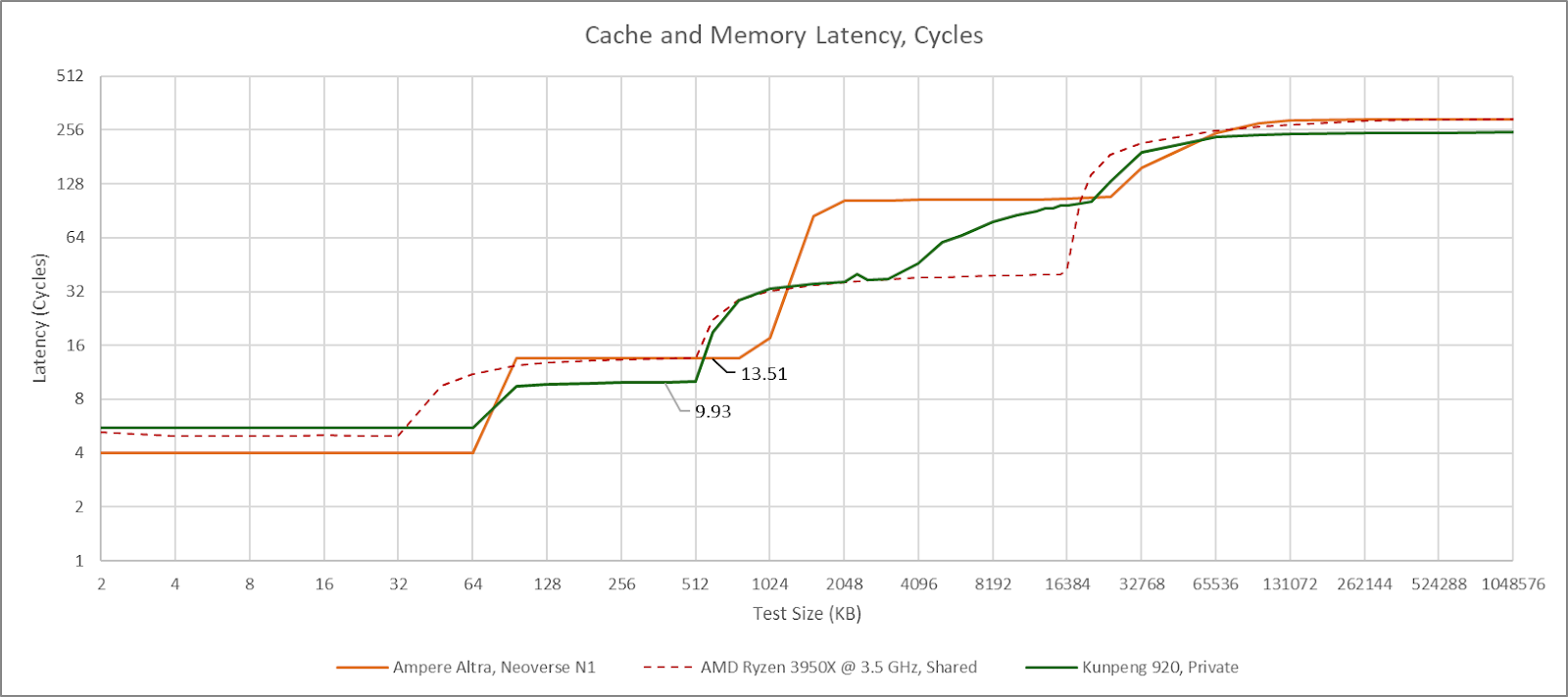
Partition mode is the default, and the only mode on the test system. Some Kunpeng 920 systems allow setting L3 cache policies in the BIOS, but the test system does not have a BIOS interface and cache control settings are not exposed through UEFI variables. With partition mode, a core sees reasonable 36 cycle L3 latency out to just under 4 MB. Latency gradually increases at larger test sizes as the private L3 portion expands to include nearby L3 slices. Finally, latency exceeds 90 cycles as test sizes approach L3 capacity.
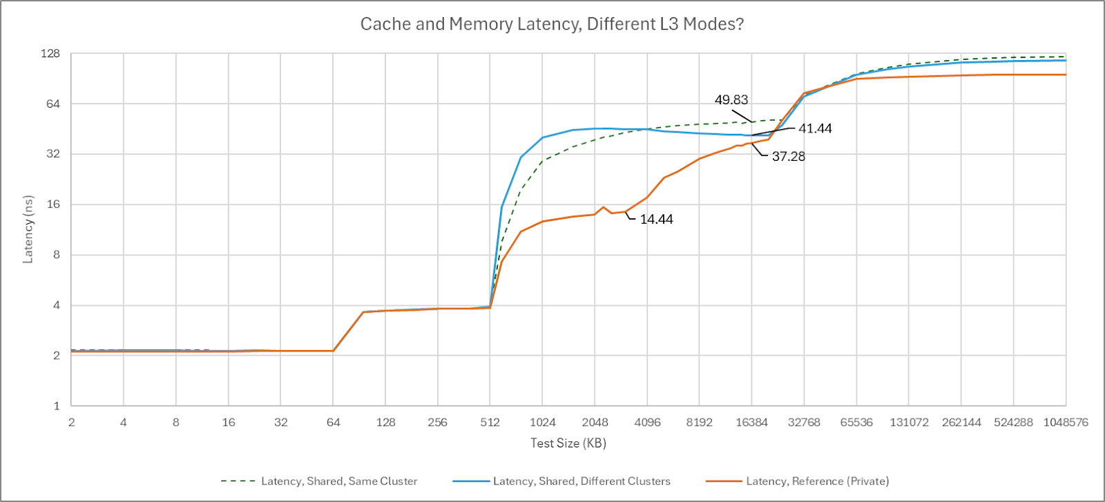
If another core traverses the same test array, L3 latency becomes uniformly high throughout its capacity range. Latency reaches the >90 cycle range even when the test array only slightly spills out of L2, suggesting the L3 is operating in shared mode. Surprisingly, data sharing between two cores in the same cluster triggers similar behavior. Perhaps the L3 enters shared mode when cachelines are in shared state, or can’t cache lines in shared state within a cluster’s private L3 partition.
This isn’t always an optimal strategy. For example, two cores sharing a 2 MB array would be better served with that array kept within private L3 partitions. Data duplication isn’t a problem if the L3 isn’t under capacity pressure in the first place. Lack of a special case for data sharing within a cluster is also baffling.
From one angle, Kunpeng 920’s partition mode is an advantage because it exploits how L3 banks are placed closer to certain cores. AMD, Intel, and most Arm chips have the same non-uniform L3 latency characteristics under the hood, but don’t try to place L3 data closer to the core using it. From another angle though, partition mode tries to cover for poor interconnect performance. Kunpeng 920 has worse L3 latency than Intel’s Sapphire Rapids when the L3 is operating in shared mode, or when a single core uses the entire L3. That’s brutal with just 512 KB of L2 per core. I lean towards the latter view because even core-private accesses to the closest L3 slice have the same cycle count latency as Zen 2’s L3, which distributes accesses across L3 banks. Zen 2 maintains uniformly low latency throughout the L3 capacity range with either a shared or private read pattern. Thus Kunpeng 920’s partition mode is best seen as a mechanism that can sometimes cover for a high latency interconnect.
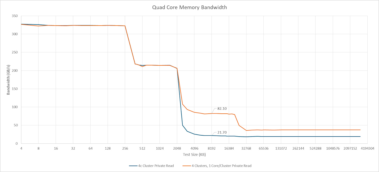
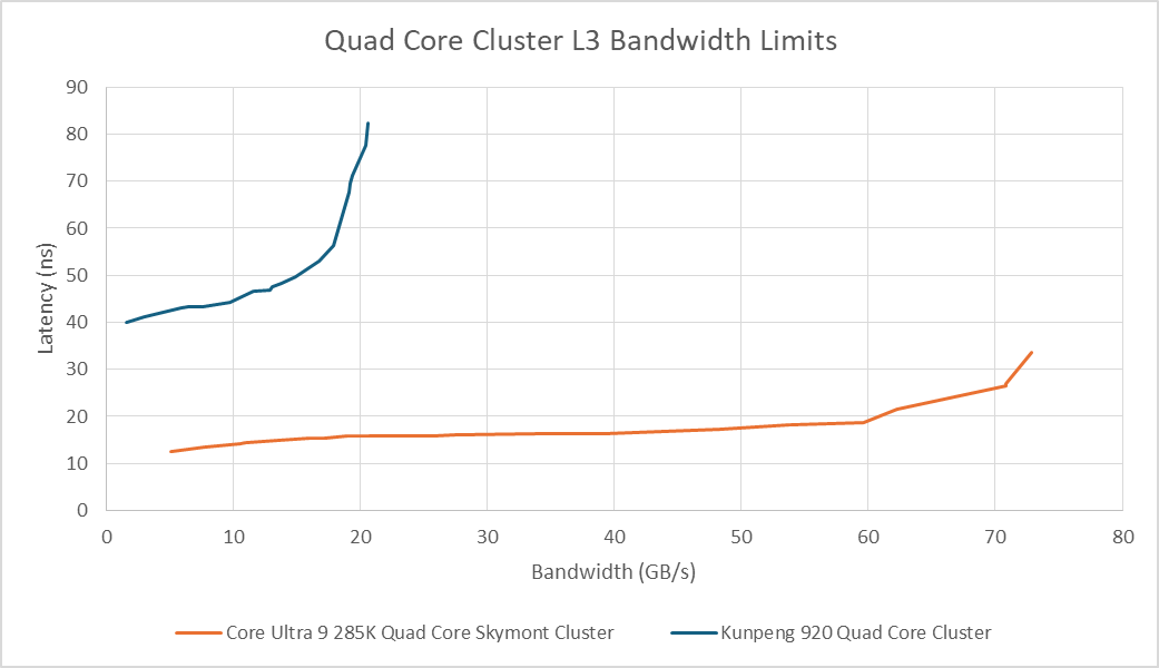
A quad core TaiShan v110 cluster can achieve 21.7 GB/s of L3 read bandwidth, so Kunpeng 920 has cluster-level bandwidth pinch points much like with Intel’s E-Core clusters. However, those bandwidth pinch points are more severe on Kunpeng 920. Bandwidth contention from sibling cores within a cluster can bring L3 latency to over 80 ns. Intel’s design also sees a latency increase, as tested on Skymont, but has overall lower latency and higher bandwidth.
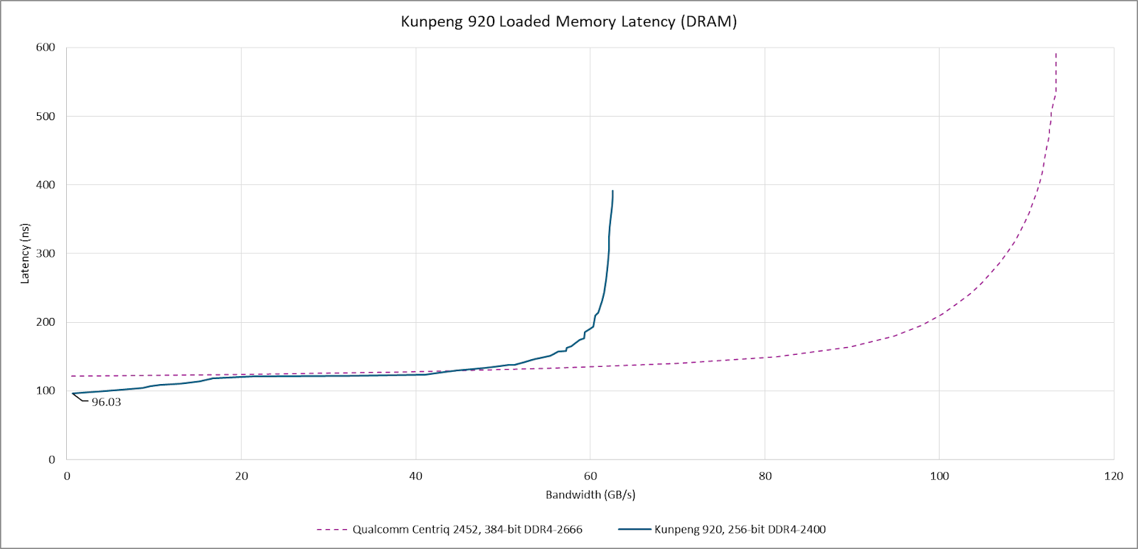
DRAM access is provided by a pair of dual channel DDR4 controllers positioned at the top and bottom edges of the compute die, which are connected to 32 GB of DDR4-2400 in the test setup. Read bandwidth was measured at 63 GB/s using a read-only pattern. Unloaded latency is good for a server chip at 96 ns, though latency quickly steps up to over 100 ns under moderate bandwidth load. Pushing bandwidth limits can send latency beyond 300 ns. While not great, it’s better controlled than the near 600 ns latency that Qualcomm Centriq can reach.
Core to Core Latency Test
Kunpeng 920 delivers reasonable latency when bouncing cachelines within a quad core cluster. Cross-cluster accesses incur significantly higher latency, and likely vary depending on where the shared cacheline is homed.
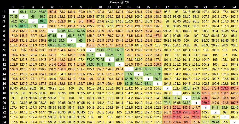
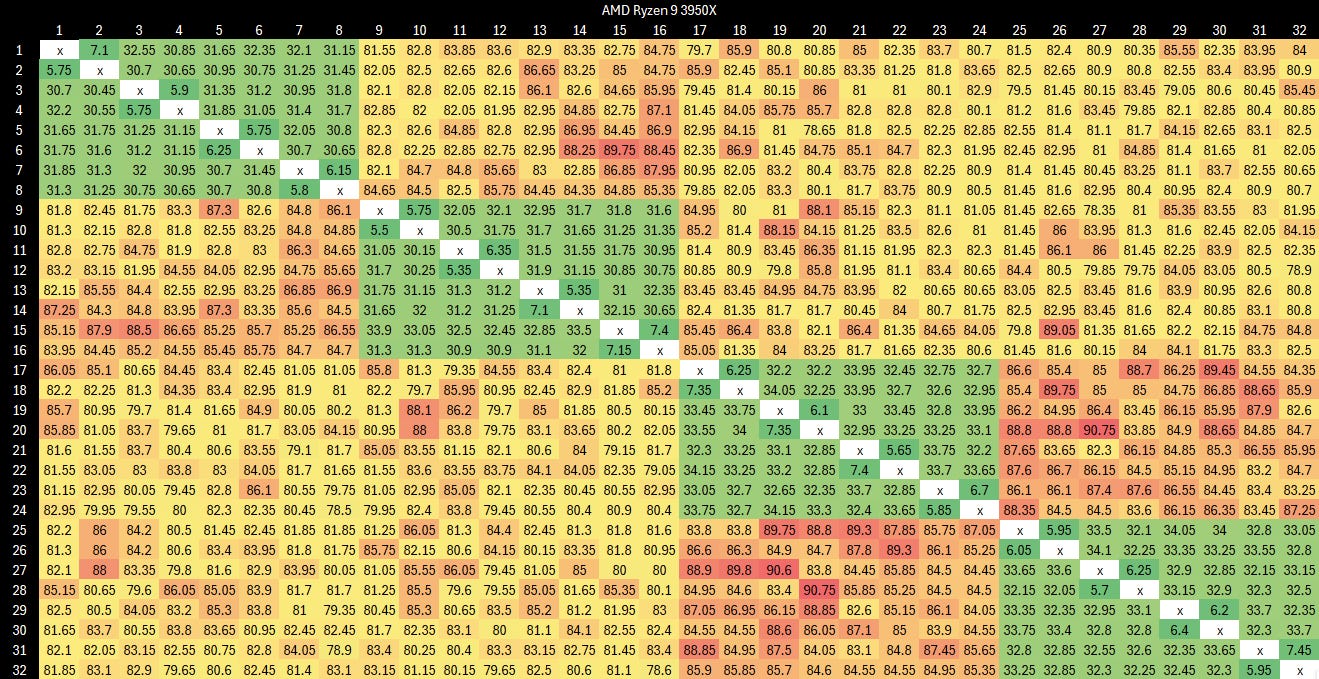
Latency is higher for both the intra-cluster and cross-cluster cases compared to AMD’s Zen 2, at least on a desktop platform.
Cache-to-cache transfers are rare in practice, and I only run this test to show system topology and to provide clues on how cache coherency might be handled. Core to core latency is unlikely to have significant impact on application performance.
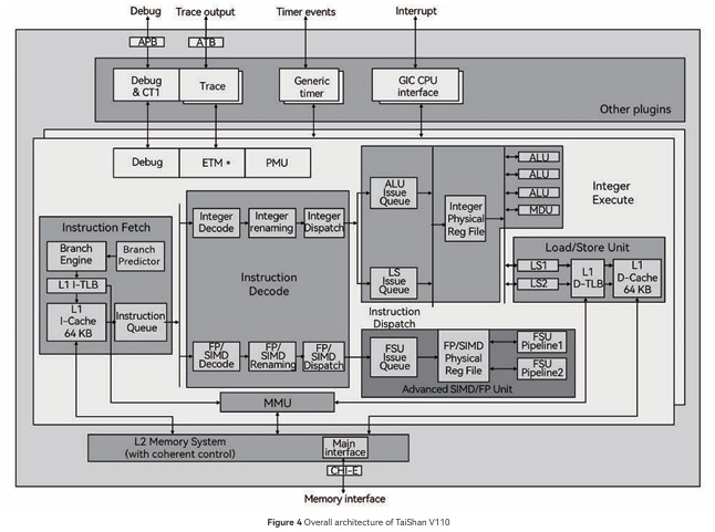
TaiShan v110 Core Overview
HiSilicon’s TaiShan v110 is a 64-bit ARM (aarch64) core with 4-wide out-of-order execution. It’s Huawei’s first custom core design. While Huawei previously used Arm’s Cortex A57 and A72 in server SoCs, TaiShan v110 does not appear to have much in common with those older Arm designs.
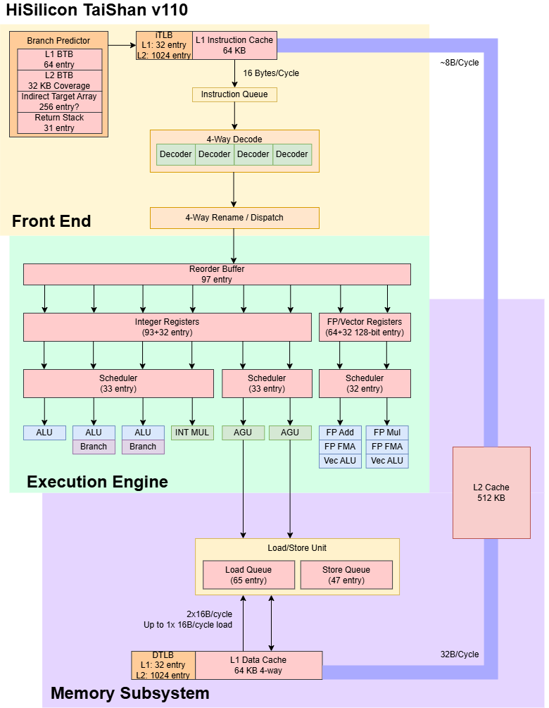
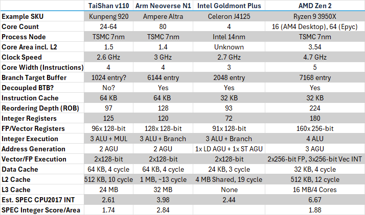
The core has modest reordering capacity, three integer ALUs, a dual-pipe FPU, and can service two memory operations per cycle. It’s broadly comparable to Intel’s Goldmont Plus from a few years before, but is slightly larger than Goldmont Plus and enjoys a much stronger server-class memory subsystem. Arm’s Neoverse N1 is another point of comparison, because it’s another density-optimized aarch64 core implemented on TSMC’s 7nm node. Neoverse N1 is also 4-wide, but has a somewhat larger out-of-order engine.
Branch Prediction
Huawei’s publications say TaiShan v110 uses a “two-level dynamic branch predictor”. A two-level prediction uses the branch address and prior branch outcomes to index into a table of predicted branch outcomes. It’s a relatively simple prediction algorithm that fell out of favor in high performance designs as the 2010s rolled around. Huawei could also be referring to a “two-level” BTB setup, or a sub-predictor that creates two overriding levels. From a simple test with conditional branches that are either taken or not-taken in random patterns of varying length, TaiShan v110 behaves a bit like Arm’s Cortex A73.
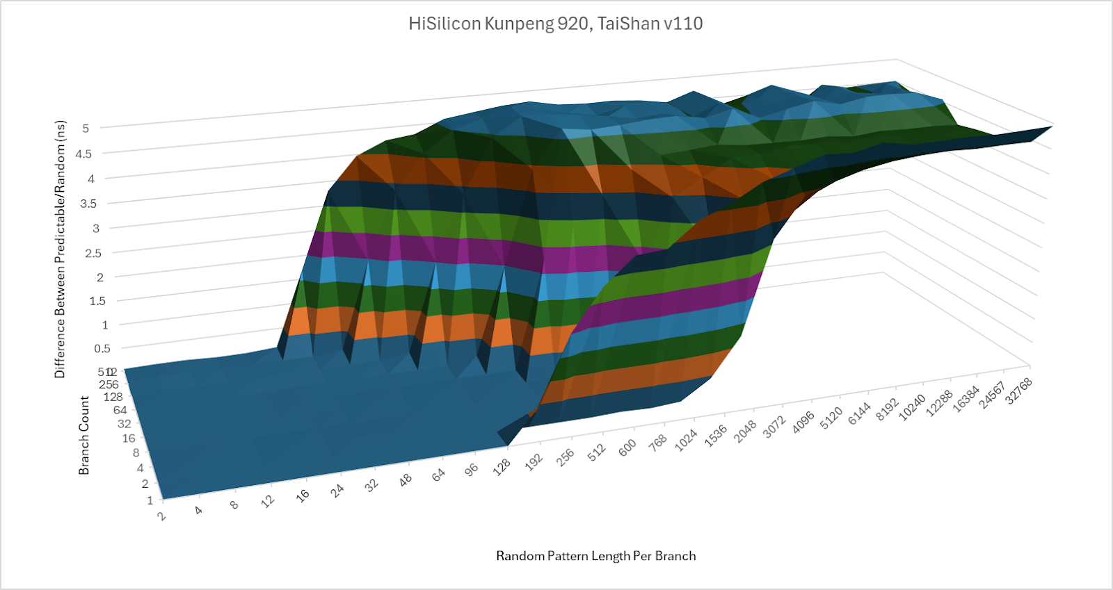
A 64 entry BTB provides taken branch targets with single cycle latency, allowing for zero-bubble taken branches. Past that, the branch predictor handles branches with 3 cycle latency as long as code fits within 32 KB and branches are not spaced too close together. Branches spaced by 16B or less incur an extra penalty cycle, and anything denser performs poorly. Spilling out of L1i dramatically increases taken branch latency. With one branch per 64B cacheline, latency reaches 11-12 cycles from L2, or beyond 38 cycles when code has to be fetched from L2. That roughly lines up with data-side L2 and private L3 latencies, suggesting the branch predictor is unable to run ahead of the rest of instruction fetch to drive prefetching.
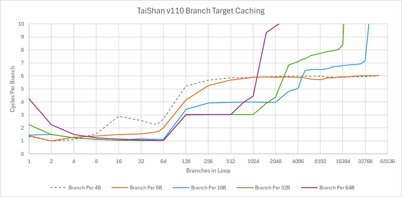
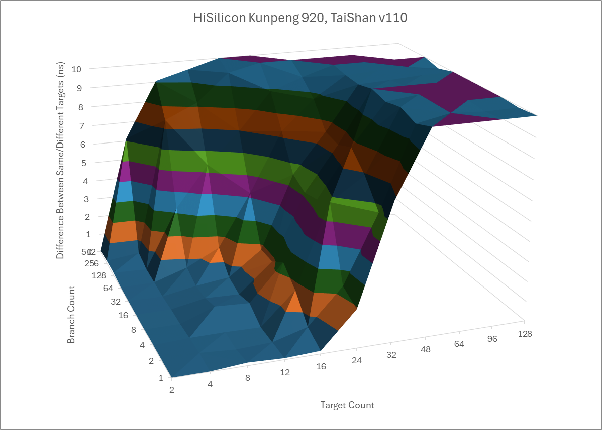
A 31 entry return stack handles returns. For the more generalized case of indirect branches, an indirect predictor can track up to 16 cycles per branch, or approximately 256 total indirect targets before taking significant penalties.
Branch prediction accuracy in SPEC CPU2017 roughly matches that of Intel’s Goldmont Plus, though Goldmont Plus takes a win by the slimmest of margins. AMD’s Zen 2 from around the same time turns in a stronger performance, and shows what can be expected from a high performance core on TSMC’s 7nm node.
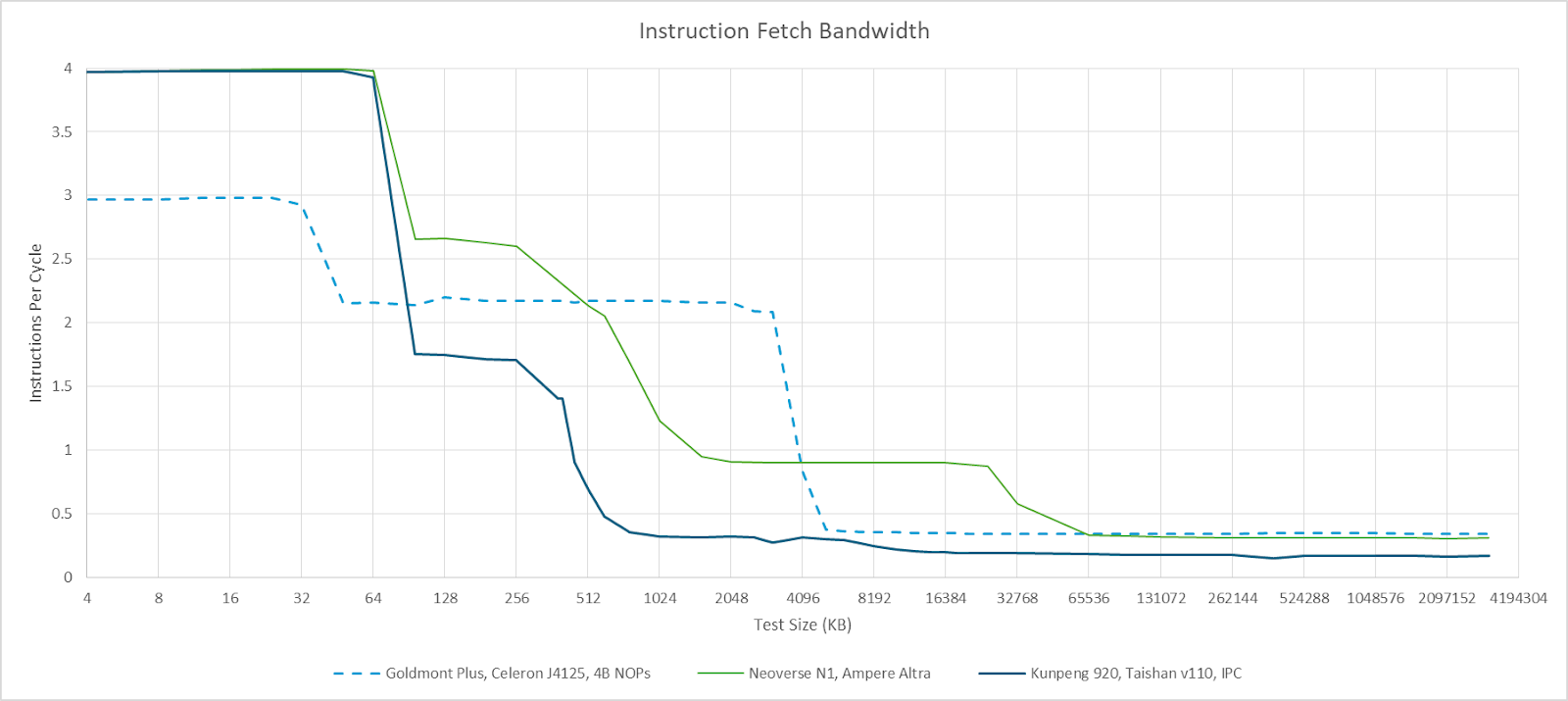
Instruction Fetch
TaiShan v110 has a 64 KB instruction cache, which can supply the core with four instructions per cycle. Instruction-side address translations use a 32 entry iTLB, which is backed by a 1024 entry L2 TLB. The L2 TLB may be shared with data access, but I currently don’t have a test written to check that. Instruction fetch bandwidth drops sharply as code spills out of L1i, to 6-7 bytes per cycle on average. That makes L2 code read bandwidth somewhat worse than on Intel’s Goldmont Plus or Arm’s Neoverse N1. Code bandwidth from L3 is very poor and is about as bad as fetching instructions from DRAM on Goldmont Plus or Neoverse N1.
Instructions are decoded by a 4-wide decoder that translates them to micro-ops. Then, the core carries out register renaming and allocates other backend resources to track them and enable out-of-order execution. The renamer can carry out move elimination.
Execution Engine
TaiShan v110 uses a PRF-based execution scheme, where register values are stored in physical register files and other structures store pointers to those register file entries. Reorder buffer capacity is similar to Intel’s Goldmont Plus, but TaiShan v110’s larger integer register file and memory ordering queues should put it ahead. The scheduler layout splits micro-ops into ALU, memory access, and FP/vector categories, and uses a separate unified scheduler for each. Each scheduler has approximately 33 entries. Goldmont Plus uses a distributed scheduler layout on the integer side, while Arm’s Neoverse N1 uses a purely distributed scheduler layout.
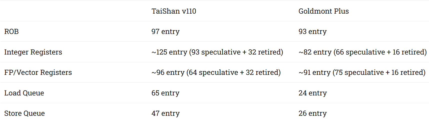
SPEC CPU2017’s workloads heavily pressure TaiShan v110’s schedulers. Scheduler entries are often a “hot” resource on any core, so that’s not unusual to see. Integer register file capacity is rarely an issue because the core has nearly enough integer registers to cover ROB capacity. TaiShan v110 renames flags (condition codes) in a separate register file with approximately 31 renames available. Flag renames are rarely an issue either, except in very branch heavy workloads like file compression and 505.mcf.
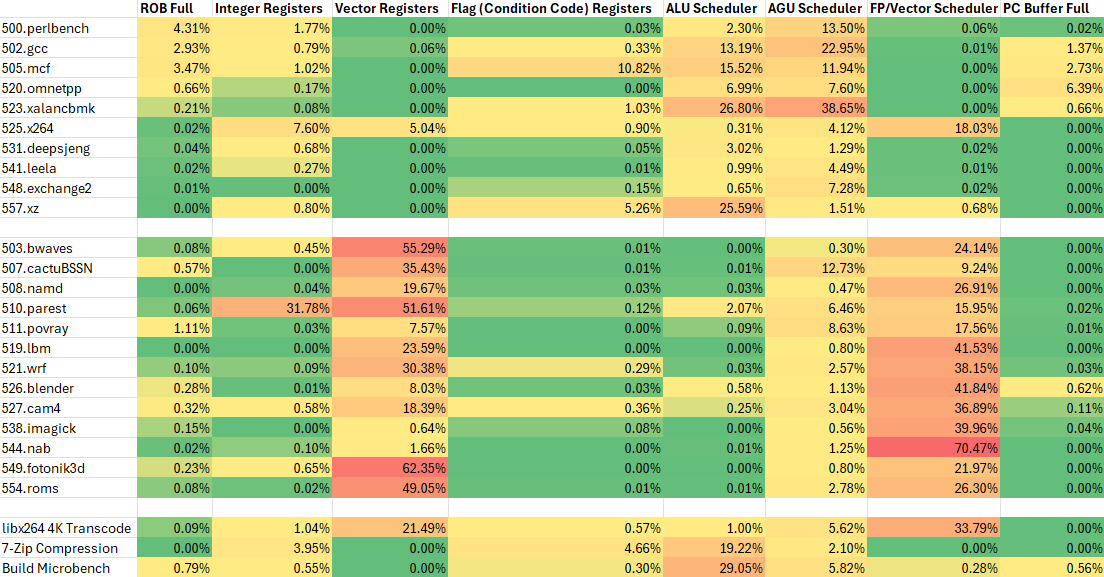
Floating point workloads put pressure on the FP/vector register file in addition to the FPU’s scheduler. TaiShan v110 likely has similar FP/vector register file capacity to Goldmont Plus, but has fewer available for renaming because aarch64 defines 32 FP/vector registers instead of 16 on x86-64. A larger register file would help better balance the core for FP and vector workloads.
Execution Ports
TaiShan v110’s integer execution side has four ports. Three are general purpose ALUs that handle simple and common operations like integer adds and bitwise operations. Branches can go down two of those ports, though the core can only sustain one taken branch per cycle much like other cores of the era. The fourth port is specialized for multi-cycle integer operations like multiplies and divides. Integer multiples execute with four cycle latency. Goldmont Plus and Neoverse N1 similarly have a 3+1 integer port setup, but both place branches on the fourth port instead of using it for multi-cycle operations. Putting branches on the fourth port may be slightly better for throughput, because branches tend to be more common than multi-cycle operations. Placing branches on a dedicated port also naturally prioritizes them because no other instruction category contends for the same port. That can help discover mispredicts faster, reducing wasted work. On the other hand, TaiShan v110’s layout likely simplifies scheduling by grouping ports by latency characteristics.
The FPU on TaiShan v110 has two ports, which is common for low power and density optimized designs of the period. Both ports can handle floating point fused multiply-add operations with 128-bit vector length with FP32 operations. FP64 operations execute at quarter rate. FP32 FMA operations have 5 cycle latency. Strangely, FP32 adds and multiplies can only be serviced by a single port each, even though both have the same 5 cycle latency as FMA operations. Vector integer adds can use both ports and have 2 cycle latency. Only one port has a vector integer multiplier.
Load/Store
Two AGU ports generate memory addresses, and provide 4 cycle load-to-use latency for L1D hits. Latency increases by 1-2 cycles with indexed addressing. Virtual addresses from the AGUs are translated to physical addresses by a 32 entry fully associative data TLB. A 1024 L2 TLB handles larger memory footprints. Hitting the L2 TLB adds 11 cycles of latency, which is slow for a low-clocked core. AMD’s Zen 2 and Intel’s Goldmont Plus have 7 and 8 cycle L2 TLB latencies, respectively. Zen 2 notably has twice as much TLB capacity at 2048 entries, and can reach much higher clock speeds.
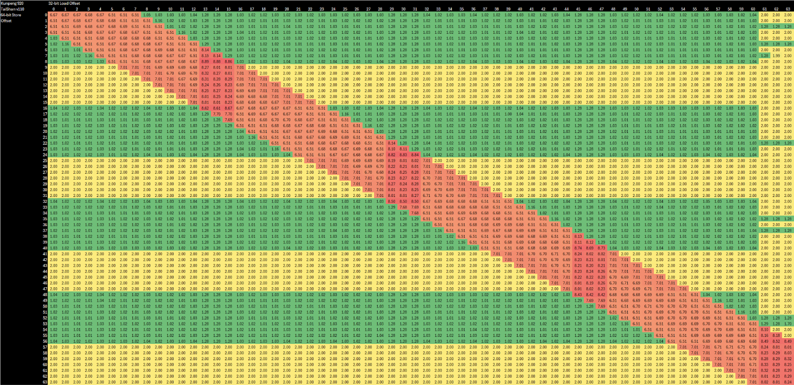
Load addresses have to be checked against prior store addresses to detect memory dependencies. Store forwarding has 6-7 cycle latency, which is remarkably maintained even when a store only partially overlaps a subsequent load. The core’s L1D appears to operate on 16B aligned blocks. Forwarding latency increases by 1-2 cycles when crossing a 16B boundary. Independent loads and stores can proceed in parallel as long as neither cross a 16B boundary.
TaiShan v110’s 64 KB data cache is 4-way set associative, and can service two 128-bit accesses per cycle. Both can be loads, and one can be a store. Data cache bandwidth is superior to Intel’s Goldmont Plus, which can also do two 128-bit accesses per cycle but is limited to one load and one store. Loads typically outnumber stores by a large margin, so TaiShan v110 should have a bandwidth advantage in practice. Neoverse N1, a newer density optimized design, has similar L1D bandwidth to TaiShan v110.
L2 Cache
The L2 Cache on TaiShan v110 has 512 KB of capacity, and is private to each core. Even though cores are arranged in clusters of four, there is no cluster-level shared cache as on Intel’s E-Cores. The L2 has 10 cycle latency, making it faster in cycle count terms than Neoverse N1 or Zen 2.
The L2 can average about 20 bytes per cycle, indicating the core likely has a 32 byte per cycle interface between the L2 and L1D. Using a read-modify-write pattern did not increase bandwidth, so the L2 to L1D interface is likely not bidirectional. Still, there’s plenty of L2 bandwidth considering the core’s large L1D and modest vector capabilities.
TaiShan v110’s L2 seems designed for high performance at the expense of capacity. Goldmont Plus takes the opposite design, using a large 4 MB shared L2 because the L2 also serves as the last level cache. Huawei may have hoped to rely on dynamic L3 partitioning to reduce average L2 miss latency, which lets the L2 design focus on speed.
Performance: SPEC CPU2017
Huawei selected SPEC CPU2017’s integer suite as a metric to evaluate TaiShan v110, because its target market includes workloads that “involve extensive integer operations.” In single core testing, TaiShan v110 pulls ahead of Arm’s Cortex A72 and Intel’s Goldmont Plus by 22.5% and 7% respectively. It’s no doubt better than cores from prior generations. But its lead over Goldmont Plus is narrow considering TaiShan v110’s process node advantage, larger last level cache, and better DRAM controllers.
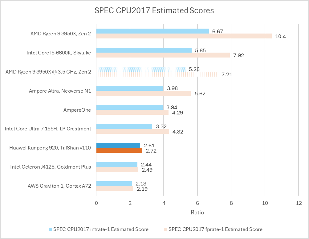
Comparing with TSMC 7nm peers puts TaiShan v110 in a tougher spot. Arm’s Neoverse N1 is 52.2% faster than TaiShan v110. AMD’s Zen 2 takes a massive lead, which is expected for a high performance design.
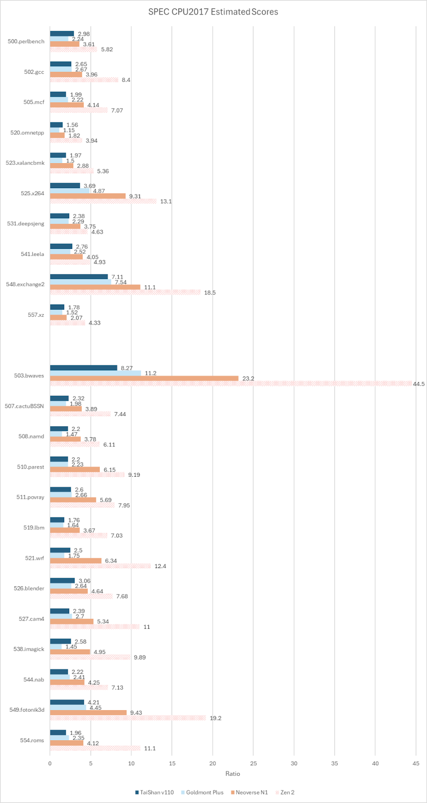
While TaiShan v110 is overall better than Goldmont Plus, it falls behind on 505.mcf, 525.x264, and 503.bwaves. In all three cases, TaiShan v110 suffered more mispredicts per instruction and worse branch prediction accuracy. Somehow, those tests challenged TaiShan v110’s predictor, even though its branch predictor achieved similar accuracy to Goldmont Plus in other subtests that stress the branch predictor, like 541.leela.
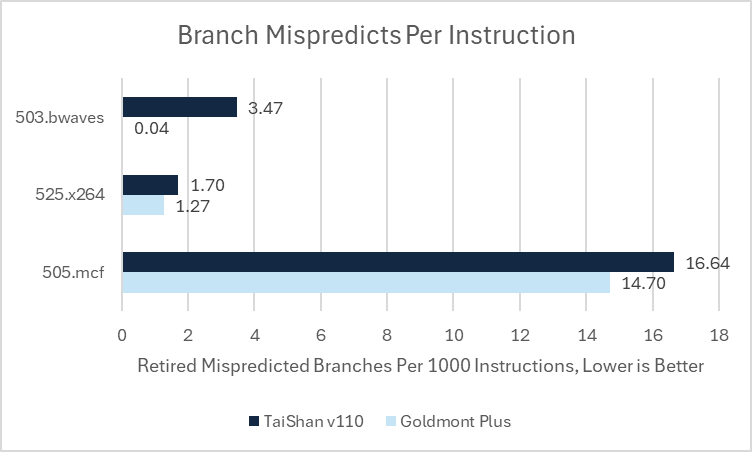
Neoverse N1 wins against TaiShan v110 in every subtest. Neoverse N1’s largest wins come from 505.mcf and 525.x264. The former sees Neoverse N1 get 15.03 branch MPKI compared to 16.64 on TaiShan v110. 505.mcf is very bound by backend memory accesses in addition to branch mispredicts, making it an overall nightmare for any CPU core. Ampere Altra’s cache setup and better branch predictor likely combine to let it outperform Kunpeng 920 by over 100%. The situation with 525.x264 is harder to understand. I suspect I got a bad run on Kunpeng 920 when getting a score report, because a subsequent run with performance counters suggests the score gap shouldn’t be so large based on achieved IPC, actual instruction counts, and clock speeds. However with time limits and a remote testing setup, there is no opportunity to follow up on that.
Regardless of what’s going on with 525.x264, Neoverse N1’s advantage is clear. N1 has an excellent branch predictor that’s nearly on par with the one in Zen 2 when taking the geomean of branch prediction accuracy across all subtests. Its out-of-order execution engine is only slightly larger than the one in TaiShan v110. But N1’s backend resources are better balanced. It has more integer-side scheduler entries and a larger FP/vector register file. TaiShan v110 often felt pressure in both areas. At the memory subsystem, any advantage from Kunpeng 920’s partition mode seems to be offset by Neoverse N1’s larger L2.
Final Words
Kunpeng 920 hosts a collection of fascinating features. It’s an early adopter of TSMC’s 7nm node in the server world, beating Ampere Altra and Zen 2 server variants to market. It uses TSMC’s CoWoS packaging, at a time when AMD opted for simpler on-package traces and Ampere stuck with a monolithic design. Dynamic L3 behavior is a standout feature when others (besides IBM) only operated their L3 caches in the equivalent of “shared” mode. I’m sure many tech enthusiasts have looked at multi-bank L3 designs on Intel and AMD CPUs, and wondered whether they’d try to keep L3 data closer to the cores using it most. Well, Huawei tries to do exactly that.
Yet Kunpeng 920 struggles to convert these features into advantages. CoWoS’s high cross-die bandwidth seems wasted if the chip isn’t set up to behave like a monolithic design to software. The L3’s partition mode provides inconsistent performance depending on data sharing behavior. L3 performance is poor when a single core needs to use most of L3 capacity or if cores share data. Zen 2’s uniformly fast L3 is more consistent and higher performance even if it doesn’t take advantage of bank/core locality. Neoverse N1’s use of a larger L2 to insulate the core from L3 latency also looks like a better option in practice. Perhaps the only advantage that came through was the flexibility of its chiplet design, which lets Huawei cover a wider variety of product categories while reusing dies.
At the core level, it’s hard to escape the conclusion that TSMC’s 7nm advantages were wasted too. Neoverse N1 targeted similar goals on the same node, and did a better job. Arm’s talent in density optimized designs really shows through. They were able to cram larger structures into the same area, including a branch predictor with a 6K entry BTB and a bigger vector register file. They were able to better tune core structures to reduce backend resource stalls in latency bound workloads. And finally, they were able to give Neoverse N1 twice as much L2 capacity while keeping it all within the same area footprint as TaiShan v110. A comparison with AMD is much harder because of different design goals. But it’s interesting that Zen 2 achieves similar area efficiency when running at desktop cores, even though increasing core width and reordering capacity runs into diminishing returns.
A comparison between those cores gives the impression that AMD and Arm took TSMC’s 7nm node and really made the most of it, while HiSilicon merely did an adequate job. But an adequate job may be enough. Huawei doesn't need TaiShan v110 to go head-to-head with Neoverse N1 and Zen 2. It needs a decent core that can keep its business going. TaiShan v110 is perfectly capable of fulfilling that role. Perhaps more importantly, HiSilicon’s early uptake of advanced TSMC tech and willingness to experiment with dynamic L3 behavior shows that HiSilicon’s engineers are not afraid to play aggressively. That means TaiShan v110 can serve a springboard for future designs, providing a path to secure Huawei’s future.
References
TaiShan v110 port assignments for micro-ops from various instructions: https://github.com/qcjiang/OSACA/blob/feature/tsv110/osaca/data/tsv110.yml
BIOS settings for a Kunpeng 920 server indicating the L3 can be statically set to use shared or private mode: https://support.huawei.com/enterprise/zh/doc/EDOC1100088653/98b06651
Huawei Research’s publication on Kunpeng 920 (starts on page 126): https://www-file.huawei.com/-/media/corp2020/pdf/publications/huawei-research/2022/huawei-research-issue1-en.pdf
Shanghao Liu et al, Efficient Locality-aware Instruction Stream Scheduling for Stencil Computation on ARM Processors
Description of Kunpeng 920’s NUMA behavior on larger SKUs, indicating each compute die acts as a NUMA node: https://www.hikunpeng.com/document/detail/en/perftuning/progtuneg/kunpengprogramming_05_0004.html
That bwaves discrepancy has got to be due to codegen differences with the x86-64 binary somehow avoiding unpredictable branches present in the AArch64 binary.
Waste of sand.