GCN, AMD’s GPU Architecture Modernization
AMD’s Terascale architecture became very competitive as it matured with the HD 5000 and 6000 series. But using GPUs for general purpose compute was trending around the 2010s and AMD didn’t want to miss out. Terascale’s SIMD engines were distant relatives of the execution units in ATI’s DirectX 9 era GPUs. They could do compute, but leveraging their power was hit or miss. Nvidia’s Fermi architecture had strong compute credentials and AMD wasn’t about to concede a potential market without a fight.
Graphics Core Next (GCN) throws out the Terascale playbook with a focus on predictable performance for general purpose compute. Terascale’s 64-wide wavefront stays around, but GCN is otherwise so different that it isn’t even a distant relative. GCN’s instruction set looks like that of a typical CPU, or Nvidia’s Fermi. Explicit scheduling information is gone in favor of shifting those responsibilities to hardware. Execution within a thread is strictly scalar, doing away with Terascale’s ability to issue multiple operations per cycle from a single thread.
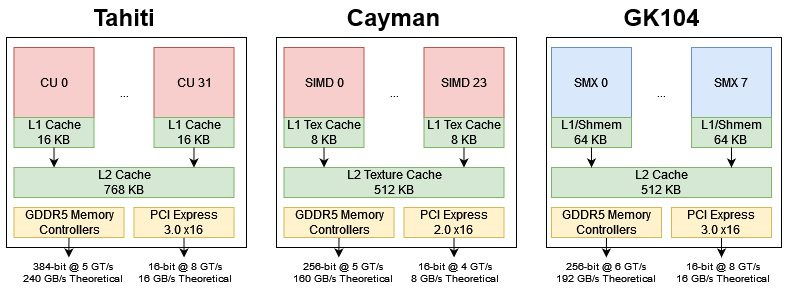
GCN first hit the market with Tahiti, a 352 mm2 chip fabricated on TSMC’s 28 nm process. Tahiti features a 384-bit GDDR5 interface to VRAM and an upgraded PCIe 3.0 link to the host, giving it more off chip bandwidth than AMD’s prior Cayman. After its introduction in 2011, GCN derived architectures served in AMD’s products for a decade. From Tahiti to Cezanne in 2021, GCN saw plenty of evolution but retained its recognizable Compute Unit structure. GCN is therefore one of the longest serving graphics architectures. Even today, GCN’s DNA lives on in AMD’s compute oriented CDNA GPUs. The CDNA line ditches some of GCN’s graphics capabilities and shifts focus to FP64, but remains a recognizable GCN derivative
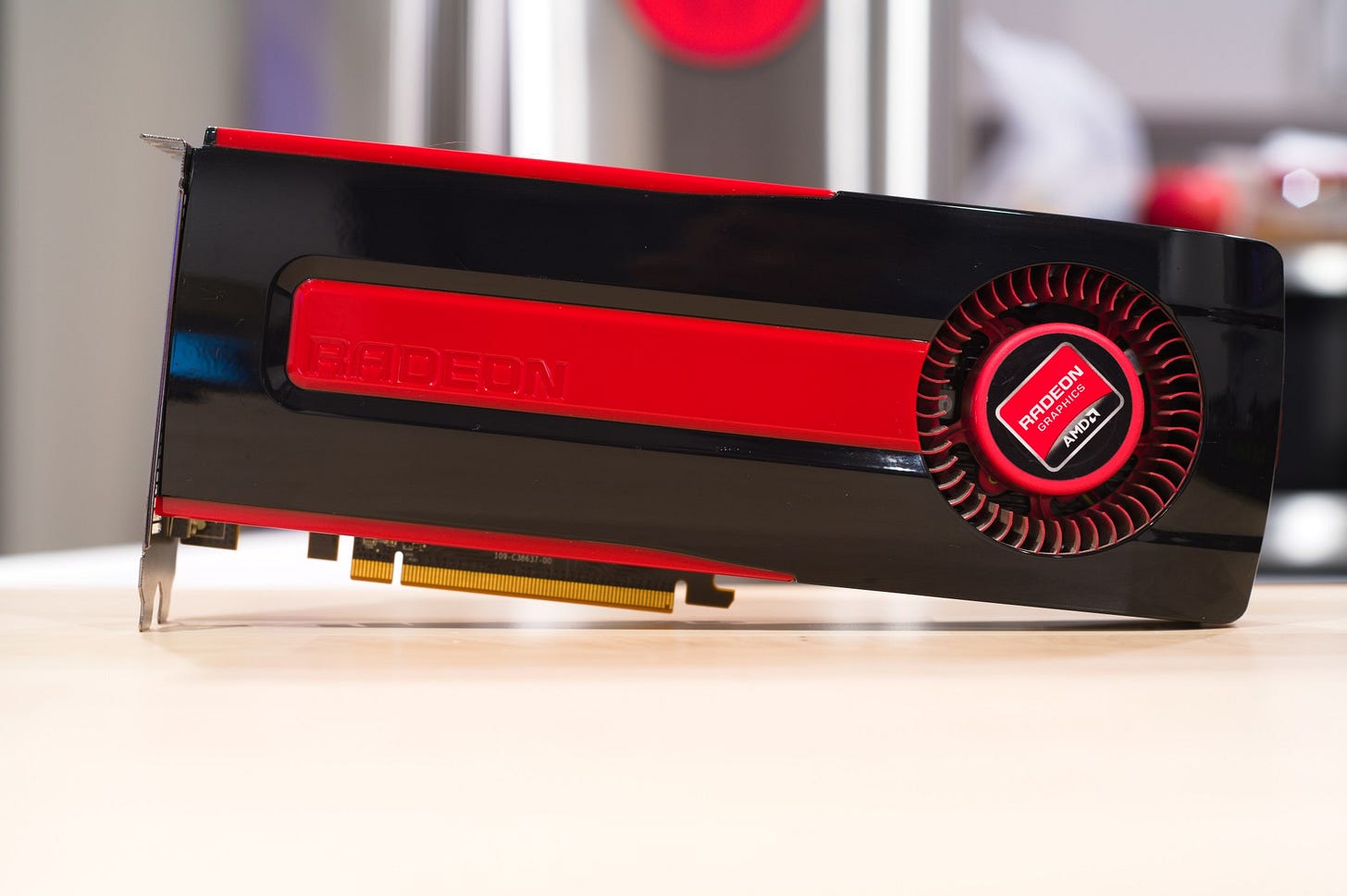
In this article, I’ll be focusing on GCN’s early days with Tahiti and Hawaii. I have data from AMD’s Radeon HD 7950, which uses a slightly cut down Tahiti chip. Hawaii is a scaled up version of GCN. It launched a year later with slight enhancements over the initial GCN architecture, and aimed to compete with Nvidia’s biggest GPUs of the time.
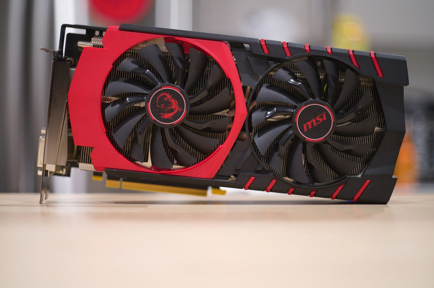
Hawaii first launched with the R9 290 series, but I’ll be looking at a R9 390. That’s a slightly cut down Hawaii chip with 8 GB of VRAM.
System Architecture
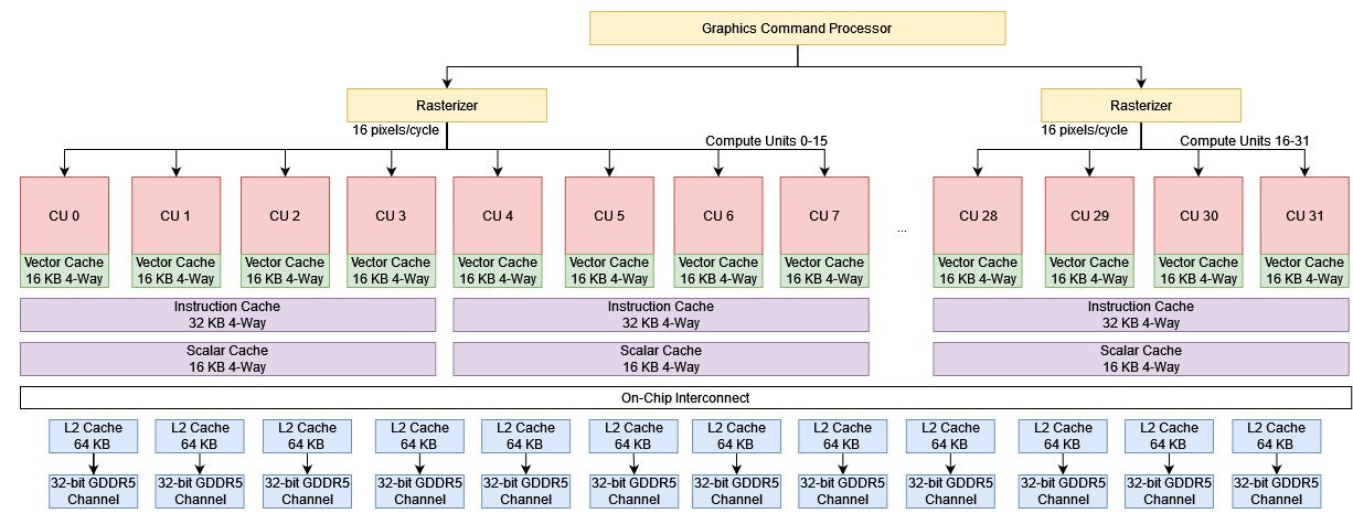
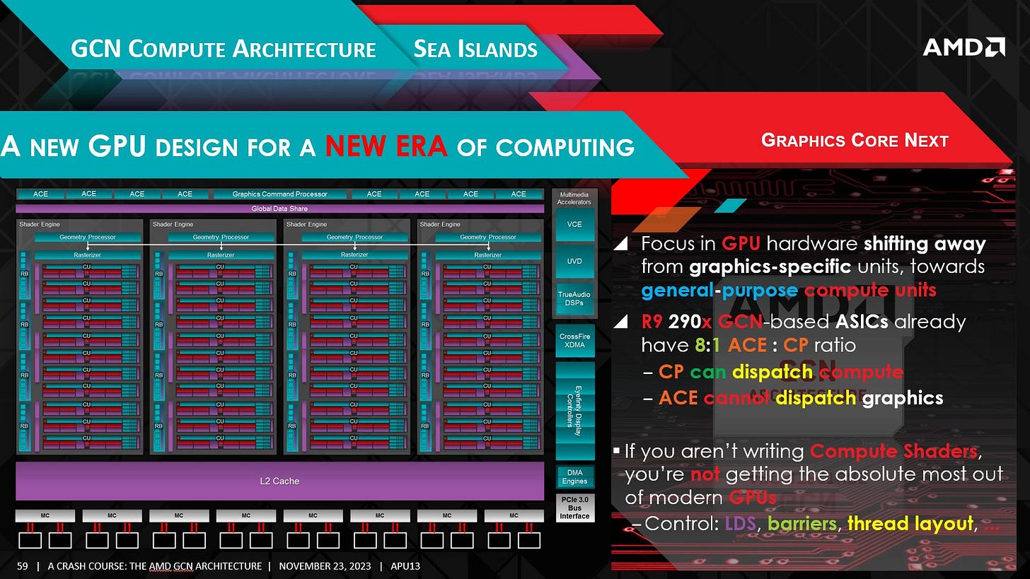
GCN’s basic building block is the Compute Unit (CU). Tahiti’s shader array consists of 32 CUs, and the HD 7950 has 28 enabled. Each CU has a private 16 KB vector cache and 64 KB local data share, but shares an instruction cache and scalar cache with up to four neighboring CUs.
The array of compute units can be fed by the Graphics Command Processor or Asynchronous Compute Engines (ACEs) depending on whether work is being submitted on the graphics or compute queue. For compute workloads, each ACE can launch one wavefront per cycle. Tahiti features two ACEs, letting it launch two wavefronts per cycle across the GPU.
For graphics workloads, GCN’s rasterizers consume screen space coordinates exported by vertex shaders. They can handle one primitve per clock and write out up to 16 pixels per cycle, so each rasterizer can launch a 64-wide wavefront every four cycles. Tahiti has two rasterizers, letting it launch one pixel wavefront every two cycles. Screen space is partitioned between the two rasterizers, mirroring Cayman’s approach with its two graphics engines. Hawaii takes this further with four rasterizers, letting it fill the shader array faster.
Compute workloads write their results to VRAM, where they can be consumed by future kernels or get copied back to the host. For graphics, pixel shader exports are sent to the render backends. Each render backend on Tahiti has a 16 KB color cache and a 4 KB depth cache. Final pixel colors are written to the memory controllers and bypass the L2 cache. Unlike Terascale, the render backends are decoupled from the memory controllers and can be scaled independently of memory bus width.
GCN’s Compute Unit
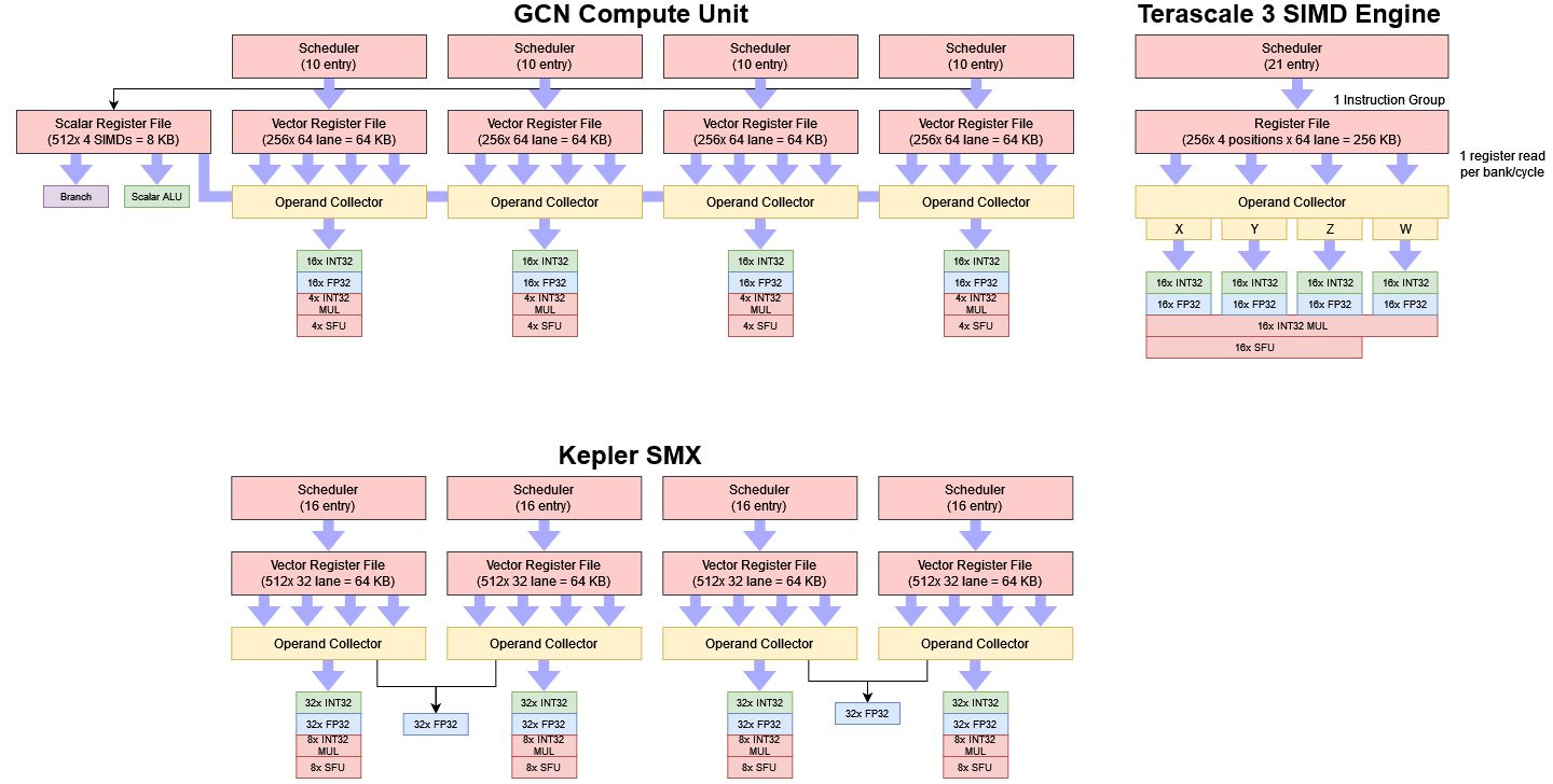
GCN’s Compute Unit is roughly analogous to Terascale’s SIMD. Both can complete 64 FP32 operations per cycle, or twice that if you count fused multiply-add operations as two. However, AMD has completely reorganized this basic building block to take VLIW bundle packing out of the picture. Instead of one big SIMD capable of quad-issuing instructions, a compute unit consists of four smaller SIMDs. Each SIMD gets its own 64 KB vector register file and 10 entry scheduler partition. Execution within a thread is now completely scalar, which means the CU can’t issue multiple instructions per cycle from the same thread. However, a CU can issue up to five instructions per cycle if multiple threads in a SIMD’s scheduler partition are ready, and each thread’s ready instruction goes to a separate functional unit.
Compute Unit Frontend
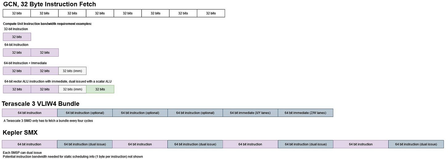
A CU’s pipeline starts by fetching instructions from a 32 KB, 4-way set associative L1 instruction cache. The instruction cache uses 64 byte lines, aligning it with common cacheline sizes on CPUs. One instruction cache instance is shared by up to four adjacent CUs, and can deliver 32 bytes per cycle to each. This is likely achieved with a quad banked setup, so bank conflicts could reduce instruction bandwidth.
Terascale 3 shared a 48 KB ALU instruction cache across up to four SIMDs, so there’s some similarity to GCN. AMD was able to cut instruction cache size to 32 KB because GCN’s variable length instructions require less storage on average. Terascale 3 used fixed length 64-bit instructions. A bundle of instructions could range from 64 to 384 bits depending on how many instructions and immediate values the compiler packs in. GCN’s instructions are 32 or 64 bits long, with an optional 32-bit immediate coming after.
Nvidia’s Kepler uses a 8 KB instruction cache private to each SMX. A private cache is better suited to handling Kepler’s high instruction bandwidth demands. A SMX needs to sustain at least 6 instructions per cycle to feed its 192 FP32 units, because each instruction on Nvidia operates on a 32-long vector of 32-bit elements. With fixed length 64-bit instructions, Kepler’s instruction cache would have to deliver 48 or 54 bytes of instructions per cycle depending on whether you count the byte of static scheduling info per instruction. GCN Compute Units only need to execute one instruction per cycle to saturate its vector execution units, both because it fewer of them and because each GCN instruction operates on a 64-long vector.
Scheduling and Instruction Issue
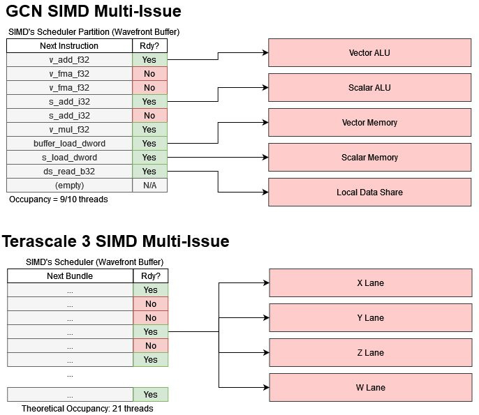
Once instructions have been fetched, they’re held in a set of instruction buffers. Each of the CU’s four SIMDs has a 10 entry buffer, letting it track instructions from up to 10 separate threads. The entire CU can thus track 40 threads (or wavefronts). With 64-wide wavefronts, a CU can have 2560 32-bit operations in flight.
Every cycle, the CU selects a SIMD and scans its 10 threads to see if any are ready for execution. GCN can achieve limited multi-issue capability by selecting multiple threads and co-issuing instructions of different categories. For example, a scalar ALU instruction from one thread can co-issue alongside a vector ALU instruction from another. In theory, a compute unit can issue 5 instructions per cycle. But such high issue rates should be rare because workloads are unlikely to have an even mix of instructions from different categories. High occupancy is essential to making most of this multi-issue strategy. If a SIMD has more threads to choose from, it has a better chance of finding multiple threads with the right mix of instructions to enable multi-issue.
GCN’s strategy contrasts with Terascale’s, which emphasizes mutli-issue from a single thread with a huge burden on the compiler. The compiler had to find instructions that were both independent and didn’t oversubscribe register file ports when packed into a bundle. GCN’s move to using thread level parallelism means the compiler can be mostly oblivious to those hardware details. Nvidia’s Kepler takes a middle ground. Register bank conflicts are handled by a hardware operand collector. The compiler was responsible for marking pairs of instructions for dual issue in the instruction stream, but dual issue was really a cherry on top. Kepler could maintain much better throughput than Terascale without having to multi-issue.
Although GCN loses the ability to multi-issue from a single thread, it can issue from a thread more often than Terascale can. A Terascale SIMD was 16-wide and could issue a bundle every four cycles, but couldn’t execute two bundles from the same thread back-to-back. Therefore, Terascale needed at least two threads in a SIMD to achieve full throughput. GCN removes this restriction, so a thread on SIMD can execute an instruction once every four cycles. Terascale could achieve higher per-thread throughput, but only if the compiler does a good job packing instructions into bundles.
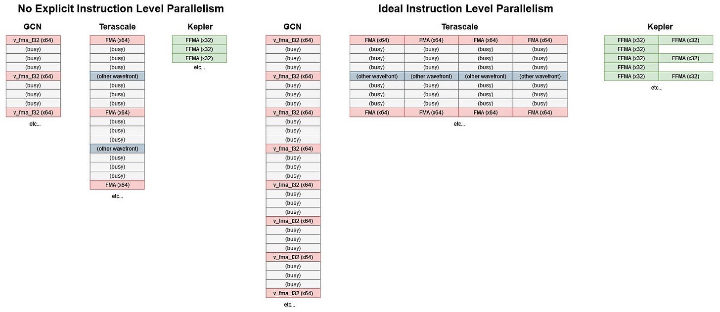
Kepler meanwhile can blaze through a single thread. It uses 32-wide waves and 32-wide execution units, so a thread can issue an instruction every cycle. Dual issue is a cherry on top. Thus Kepler can maintain decent throughput in the face of low occupancy and limited thread-level parallelism.
Register Files
A selected instruction reads its inputs from the register files. In GCN, a Terascale SIMD’s giant 256 KB register file is split into four 64 KB register files, one for each GCN SIMD. GCN’s register files are almost certainly banked structures, but should suffer less from register bank conflicts than Terascale. Assuming its still a quad banked register file, GCN would have four inputs available to feed an instruction that potentially needs up to three inputs (for a fused multiply-add). Bandwidth demands on the vector register file can be lower if an instruction takes an input from the scalar registers or an immediate value in the instruction stream. On top of that, GCN likely has an operand collector that can smooth out demands for register file bandwidth in case of occasional bank conflicts.
Terascale required intricate scheduling and register assignment to get good utilization. Each VLIW lane could only write back to its corresponding register file bank, and any register bank conflicts on the read side could reduce VLIW packing. Kepler requires even more effort to fully optimize because there isn’t enough register file bandwidth to feed FMA operations across all of a SMX’s FP32 units.
Besides the vector register file, a GCN CU has a 8 KB scalar register file. Programs can reduce vector register usage and achieve higher occupancy if they can store some variables in scalar registers.
Execution Units
Each SIMD in GCN has a 16-wide execution unit. Common FP32 operations and integer adds execute at full rate, while 32-bit integer multiplies and special functions execute at quarter rate. Theoretical throughput is similar to Terascale 3’s. But instead of needing four instructions packed into each bundle to saturate the compute units, GCN needs at least four threads active to fill its four SIMDs.
Terascale’s branch unit gets transformed into a scalar ALU. Even though GPUs are primarily vector processors, they still need to handle control flow and addresss generation. Those operations are often constant across a vector, so a scalar ALU can offload those computations. Moving those scalar operations to a dedicated unit helps reduce load on the vector ALUs and improve power efficiency.
Compared to Kepler’s SMX, GCN’s CU is smaller and offers less throughput. Tahiti compensates for this by having four times as many CUs as GK104 has SMX-es.
Hawaii scales out the shader array, letting it achieve over 5 TFLOPS of FP32 throughput. As a sign of future trends however, Hawaii’s FP64 performance falls behind Tahiti’s. GCN’s FP64 throughput can be configured from half rate to 1/16 rate. Tahiti is configured with 1/4 rate FP64 execution in line with GCN’s initial compute aspirations. AMD started investing less into FP64 execution as it became clear that GPU compute wouldn’t have a major role in client applications. So, Hawaii uses a more pedestrian 1/8 FP64 rate. But even at 1/8 rate, AMD’s client cards have a substantial FP64 performance lead over their Nvidia counterparts.
Compute Unit Data Caching
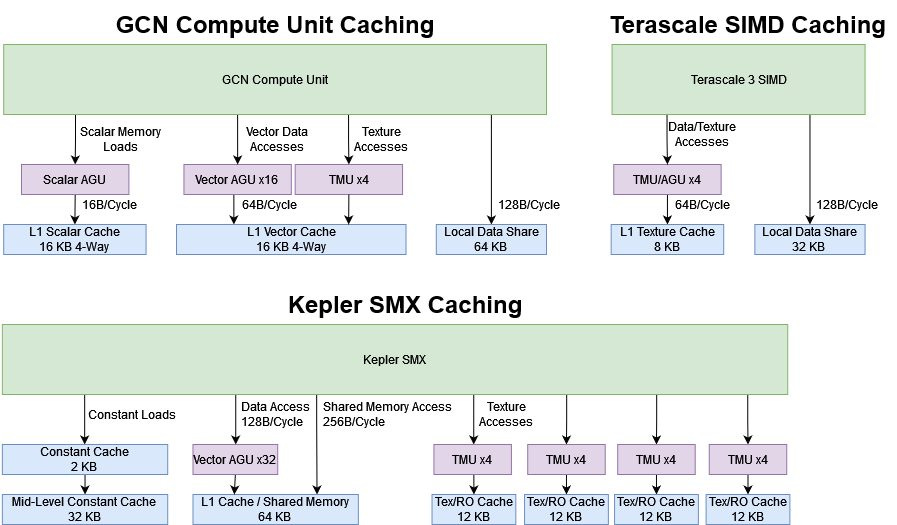
AMD has revamped the cache hierarchy to fit general purpose workloads rather than focusing exclusively on graphics. A 16 KB 4-way set associative vector cache acts as the CU’s primary data cache. It uses a LRU replacement policy, 64B lines, and can feed the compute unit with 64 bytes per cycle. Terascale’s 8 KB read-only texture cache could deliver the same per-cycle bandwidth, but GCN enjoys twice as much caching capacity and lower latency access.
GCN’s vector cache supports writes too. The L1 cache is a write-through, write-allocate design. It’s not as good as write-back caches in most CPUs, but the L1 can still help coalesce writes before they’re passed to L2.
While GCN massively improves over Terascale, Kepler still offers lower latency vector accesses. AMD hopes to mitigate this by optimizing some memory accesses to use the scalar path.
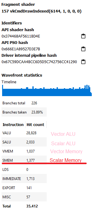
Scalar memory accesses are serviced by a 16 KB 4-way scalar cache shared by up to four neighboring CUs. The scalar cache can deliver 16 bytes per cycle to each CU and is optimized for low latency. Scalar cache hits have a latency of just under 50 ns, which is very fast for the GPU world at this time. It’s worlds apart from the 200+ ns latency of Terascale’s texture cache, and faster than any of Kepler’s caches except for its tiny 2 KB constant cache.
Next to Terascale, GCN’s caching strategy within the Compute Unit is modern and flexible. Besides being a massive improvement for compute workloads, GCN’s changes should help graphics too. Increasing texture caching capacity from 8 KB to 16 KB should reduce load on the chip-wide interconnect, and lower latency means the GPU needs less work in flight to maintain good performance.
Nvidia’s Kepler architecture dips into both the old and new worlds with a caching strategy similar to Fermi’s. Read-only texture cache are still around. But Kepler also has a separate L1 data cache, which shares storage with scratchpad memory. If that wasn’t enough, Kepler SMX-es have a private two-level constant cache setup too. The constant cache has some functionality overlap with GCN’s scalar cache. But unlike Fermi, Nvidia’s compiler no longer tries to use the constant cache for memory accesses that are constant across a wave. You have to explicitly mark memory with __constant qualifier to use the constant cache hierarchy.
The result is that Kepler has three separate data caching paths, each with enough capacity to stand on its own. This caching strategy lets Nvidia specialize each cache to fit a certain workload type. Texture caches have incredibly high 96-way associativity3 and the constant cache provides very low latency. But separate caches for everything costs area. A SMX has 146 KB of caches and scratchpad memory.
For comparison, a GCN Compute Unit has 80 KB of private data caches and scratchpad memory. That figure goes up to 84 KB if you divide the 16 KB L1 scalar cache across 4 CUs.
Local Memory
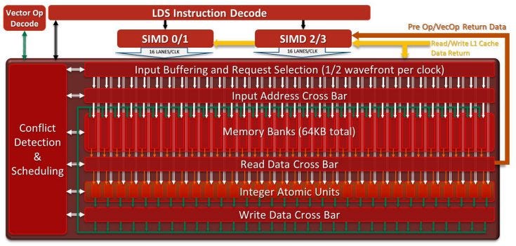
Besides the global memory hierarchy, each GCN Compute Unit has a 64 KB software managed scratchpad called the Local Data Share (LDS). OpenCL refers to this memory type as “Local Memory”. The LDS is structured much like the one in Terascale but with twice as much capacity. It consists of 32 banks, each capable of reading out a 32-bit element per cycle for a total of 128 bytes per cycle of bandwidth.
Nvidia’s Kepler dynamically allocates scratchpad and L1 cache storage out of a 64 or 128 KB block of SRAM, depending on whether you’re looking at the GK104 or GK210 variant. Nvidia refers to scratchpad memory as “Shared Memory”. Like AMD’s implementation, Nvidia’s Shared Memory consists of 32 banks, but each bank is 64 bits wide. That gives Kepler 256 bytes per cycle of local memory bandwidth, making it better suited to handling 64-bit data types.
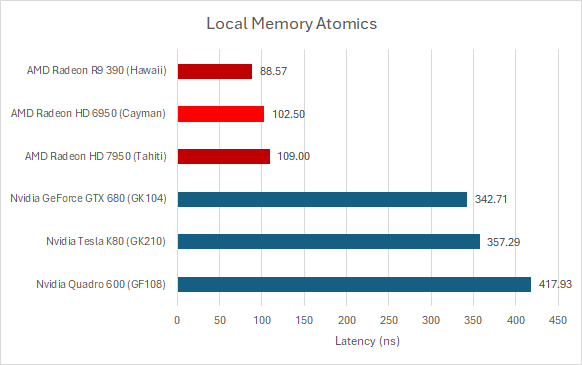
As covered before, GCN turns in a surprisingly poor performance when pointer chasing within the LDS. Tahiti is worse than Cayman (Terascale 3). Hawaii does better, but is still far off from Nvidia’s contemporary architectures.
Where AMD does have an advantage is in synchronizing threads through the LDS. Integer atomic units built into the LDS help speed these operations up. Nvidia’s Fermi and Kepler architectures don’t have an equivalent. Their Shared Memory is fast, but performance with atomics has a lot of room for improvement.
L2 Cache
Like most GPUs, GCN features a L2 cache shared across the GPU. The L2 helps catch L1 misses, and is divided into independent slices to deliver high bandwidth. Each slice has 64 or 128 KB of caching capacity and is attached to a memory controller channel. Tahiti and Hawaii appear to use 64 KB slices. Every cycle a slice can read out 64 bytes, so Tahiti’s L2 should have 768 bytes per cycle of bandwidth. The HD 7950 therefore has 710 GB/s of theoretical L2 bandwidth at its 925 MHz boost clock. At 1 GHz, the R9 390 has 1 TB/s of L2 bandwidth.
Terascale has a similar L2 slice configuration with 64 KB slices, each providing 64 bytes per cycle. However, Terascale’s L2 is a read-only texture cache. GCN’s L2 is a modern write-back design. A write-back cache only propagates writes down to the next level when the line is evicted, letting it absorb write bandwidth. In addition, GCN’s L2 slices can handle atomic operations. Atomics on Terascale would get handled at separate, smaller read-write caches and performed poorly.
Remarks on GCN’s Memory Subsystem
Terascale’s caches were built around graphics. Shader programs weren’t expected to write much to memory, and their outputs were sent to specialized on-chip buffers. Vertex shaders would export to the parameter cache and position buffer, while pixel shader would send their output to the ROPs.
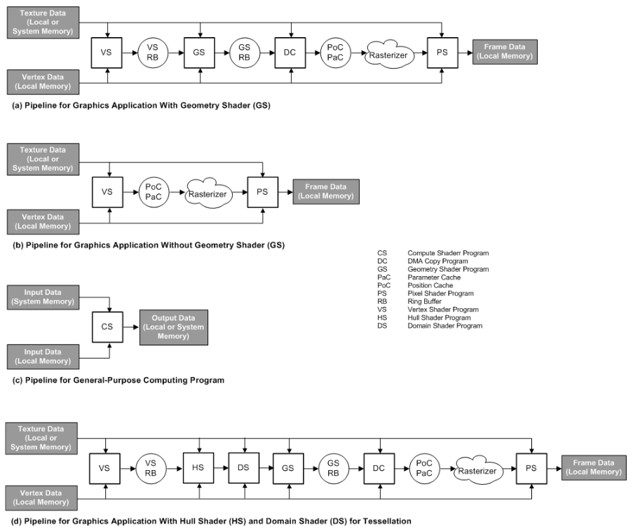
Compute programs were shoehorned into this existing structure. If you told Terascale to fetch data from memory in an OpenCL kernel, the compiler would emit a vertex fetch or texture sampling clause. The primary L1/L2 caches were read-only texture caches, so write bandwidth was poor.
GCN modernizes the cache hierarchy, and the cache setup resembles what you’d find on a GPU today. The main L1/L2 caches get write support. 64-byte cachelines are standard across all caches, making for easy data sharing with the CPU. They were virtually addressed too, making TLB misses impossible as long as you hit in cache. Cache latency and bandwidth both saw dramatic improvements over Terascale. In the 28 nm era, GCN gave AMD a large bandwidth lead. It’s the reverse of the 40 nm era, where Fermi often had more bandwidth than Terascale cards.
As AMD continued to iterate on GCN, the cache hierarchy saw further modernization. The read-only scalar cache gained write support in GCN Generation 3. Vega came after GCN Generation 3, and put the Command Processor and Render Backends in front of the L2. That helped cut down L2 flushes and amplified write bandwidth.
Despite radical changes, some Terascale vestiges remain. Instruction and scalar caches were shared by groups of four Compute Units, helping reduce die area spent on caches. It’s a clear contrast to Kepler’s approach, where designers pulled all the stops on making per-SMX caches. Partly because of this, GCN maintained very high compute density just as Terascale did against its contemporary Nvidia competition.
Compute Performance (VkFFT)
VkFFT implements Fast Fourier Transforms (FFTs) in several different GPU compute APIs. It’s a modern and currently maintained project, and GPUs from the early 2010s have trouble finishing a full benchmark run. But everyone gets through the first few subtests, and there’s enough data to show GCN’s compute potential. VkFFT can be quite memory bound, and GCN’s large memory bus lets it shine.
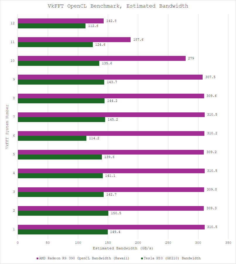
The HD 7950 does well against the GTX 680. Hawaii in the R9 390 extends that advantage. VkFFT also prints out estimated bandwidth, and those figures demonstrate what a giant 512-bit GDDR5 bus can do.
Unfortunately the Tesla K80 couldn’t participate in the Vulkan benchmarking because I couldn’t get Vulkan working on that cloud instance. Fortunately, OpenCL runs on just about everything, and VkFFT can use that as well.
When big GCN faces off against big Kepler, GCN’s incredible compute density and high memory bandwidth keep it ahead with every subtest. GK210’s 384-bit bus is outdone by Hawaii’s 512-bit one. To top it off, Hawaii also clocks faster at just above 1 GHz. The Tesla K80 runs around 875 MHz because the GK210 chip has to fit into a 150W power envelope.
VkFFT’s estimated bandwidth numbers again showcase GCN’s bandwidth advantage. The Tesla K80 only has 240 GB/s of theoretical bandwidth for each GK210 chip compared to the R9 390’s 384 GB/s. VkFFT isn’t cache friendly when profiled on RDNA 2, with the RX 6900 XT’s 4 MB L2 barely seeing any hits. The K80 and R9 390 are likely in a similar situation.
A Word on Graphics Performance
For certain compute workloads, GCN’s compute density and high memory bandwidth can let it take a large lead over Nvidia’s Kepler architecture. However, graphics workloads can be a different story. GCN’s large shader array does well with large work sizes with long durations. Some graphics workloads like full-screen pixel shaders fall into this category. However, smaller work sizes can hand Kepler the advantage.
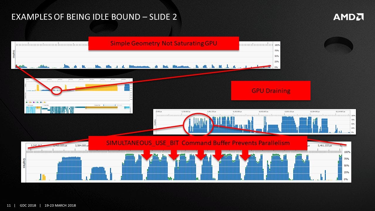
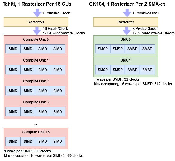
Kepler spends more area on fixed function graphics hardware relative to compute. GK104 has four rasterizer partitions, each with two SMX-es. If Kepler keeps the same rasterizer throughput as Fermi, each rasterizer can consume one primitive per clock and output 8 pixels per clock. To access Kepler’s full compute throughput, each SMX needs at least one wave assigned to each of its four scheduler partitions. Assuming no throughput loss from small triangles, the rasterizer can create the minimum amount of pixel work required to access all of Kepler’s compute potential in 32 cycles. Kepler’s full occupancy of 16 waves per SMX scheduler partition would take at least 512 cycles to reach.
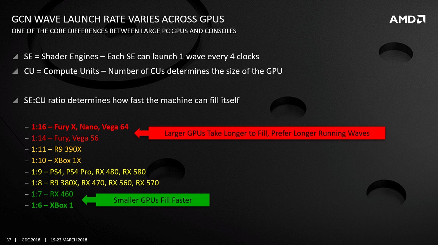
Tahiti has two rasterizers to feed an array of 32 Compute Units, or one rasterizer per 16 CUs. Each rasterizer can consume one primitive per clock and create a 64-wide wave of pixel work every four cycles. Like Kepler’s SMX-es, GCN’s Compute Units need at least one wave assigned to each SIMD to achieve full throughput. The rasterizer will take 256 clocks to do so. Reaching maximum occupancy would take 2560 clocks.
Hawaii improved this situation by going up to four rasterizers. With 11 CUs per rasterizer, second-generation GCN could reach one wave per SIMD in 176 cycles, and full occupancy in 1760 cycles. Then, larger GCN implementations like Vega 64 and Fury X expanded the shader array again, bringing the SE to CU ratio back to 1:16.
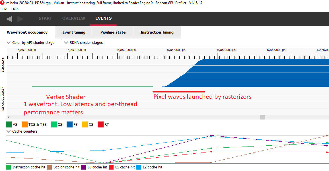
Per-thread performance is another issue. Graphics rendering can involve sequences with limited parallelism. Compared to Terascale, GCN may offer more consistent per-thread performance. But Kepler can give more execution resources to a single thread, and that can matter in sequences with lots of small draw calls.

Therefore, high end GCN GPUs often fared well at higher resolutions. Rendering more pixels means more parallelism, which makes thread launch rate and per-thread execution time less important compared to GPU-wide throughput.
Final Words
GCN is a thoroughly modern architecture. The design’s scheduling, execution unit layout, and cache setup have more in common with RDNA 3 and Nvidia’s Ada Lovelace than its direct predecessor, Terascale 3. Like recent GPUs, GCN’s design is well oriented towards compute as well as graphics. However, AMD’s move to emphasize compute did not pay off. GCN’s general purpose design didn’t matter much next to Nvidia’s ecosystem advantage. CUDA matured before OpenCL and arrived with a set of pre-optimized libraries. Worse, GPU compute did not take off in the consumer world. Gaming still mattered most.
Rasterized graphics continued to dominate gaming in the early to mid 2010s. AMD scaled out GCN’s work distribution hardware in Hawaii, but Nvidia countered with huge gains in Maxwell and Pascal. GCN still struggled to match them in both performance and power efficiency.
But GCN’s design is vindicated by modern trends, even if that’s of little comfort to AMD in 2012. Fixed function graphics hardware continues to be important, but games have gradually trended towards using more compute. Raytracing is a well publicized example. It’s basically a compute workload and doesn’t use the rasterizer. But even without raytracing, compute shaders are quietly playing a larger role in modern games. Modern designs have adopted elements of GCN’s design. RDNA keeps the scalar datapath and uses a similar instruction set. Nvidia added a scalar path (called the uniform datapath) to their Turing architecture and kept it in subsequent designs.
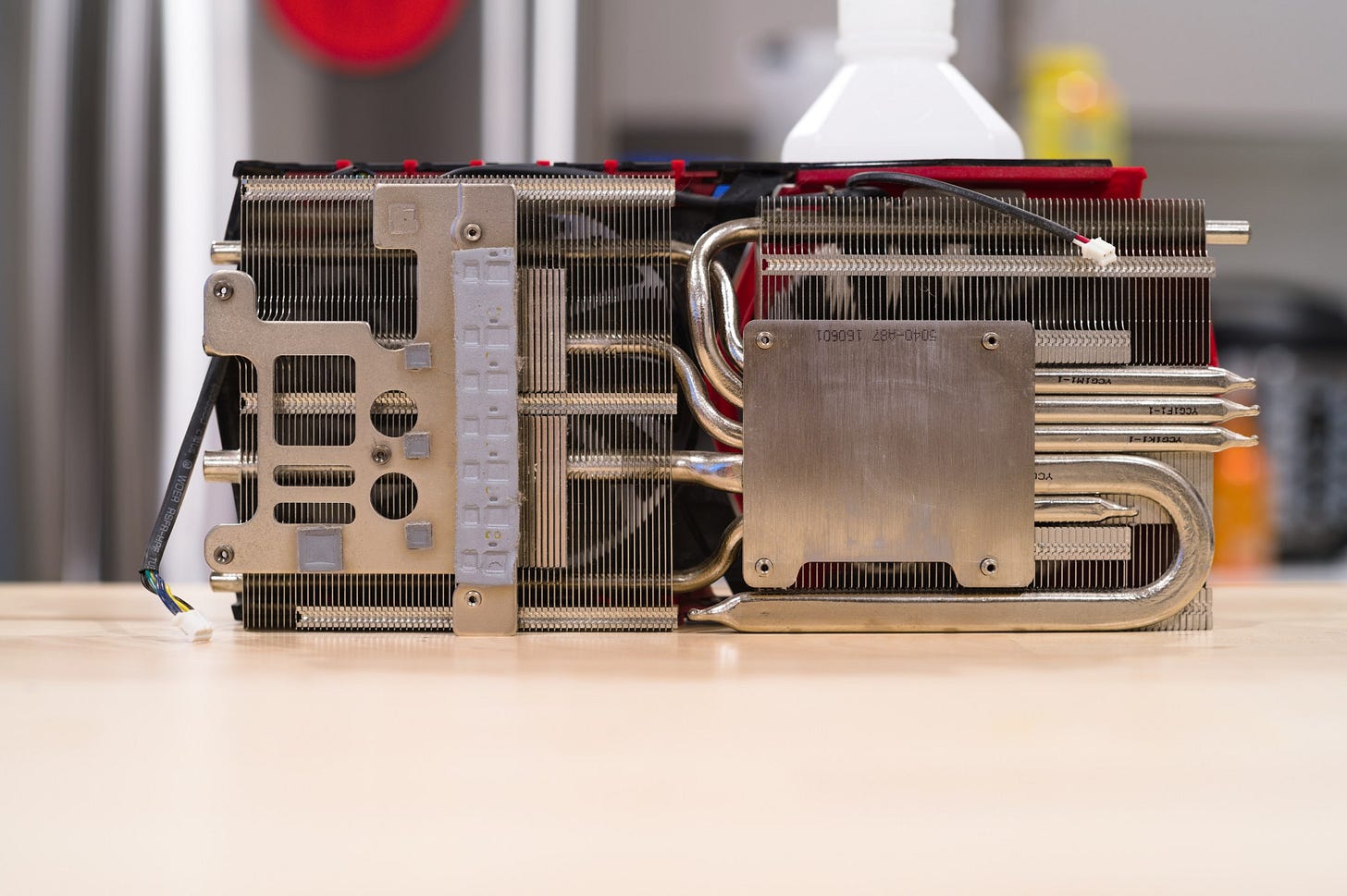
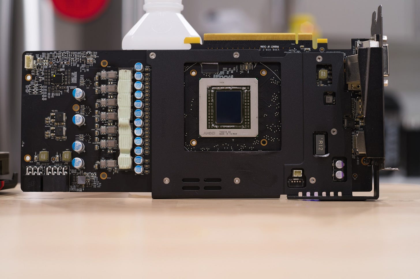
Today, the HD 7950 is more workable than the GTX 680 thanks to its higher VRAM capacity. GCN’s design also favors large, long running kernels because that lets GCN’s large shader array shine while placing less emphasis on how fast the rasterizers can launch wavefronts to fill it. That puts Tahiti in a better position to cope with the increased shader workload presented by newer games. The same applies to the R9 390. I received that card a few months ago after a friend of a friend retired it, but not because the card wasn’t powerful enough. Rather, the R9 390 had served for so long that the thermal paste had dried out, resulting in extreme throttling with roaring fans.
If you like our articles and journalism, and you want to support us in our endeavors, then consider heading over to our Patreon or our PayPal if you want to toss a few bucks our way. If you would like to talk with the Chips and Cheese staff and the people behind the scenes, then consider joining our Discord.
References
AMD Graphics Core Next (GCN) Architecture
Paulius Micikevicius, GPU Performance Analysis and Optimization
Xinxin Mei, Xiaowen Chu, Dissecting GPU Memory Hierarchy through Microbenchmarking


