Examining Intel's Arrow Lake, at the System Level
Arrow Lake is the codename for Intel's newest generation of high performance desktop CPUs. Its highest end offering, the Core Ultra 9 285K, implements eight Lion Cove P-Cores and 16 Skymont E-Cores. This site has already covered the Lion Cove and Skymont architectures in articles on Intel's Lunar Lake mobile chips. Therefore, I'll cover Arrow Lake's system architecture here, as well as differences from Lunar Lake. Because Arrow Lake is a high performance desktop part, its system architecture is focuses on delivering performance rather than shaving off every last watt.
For comparisons, I’ll have data from my Meteor Lake laptop. I also have a Zen 5 chip now, which was sampled by AMD and Cheese (George) has kindly sent over to me. I’ve dropped the 9900X into my daily driver after a BIOS update, so it should be representative of someone doing an in-socket upgrade.
Chiplet Setup
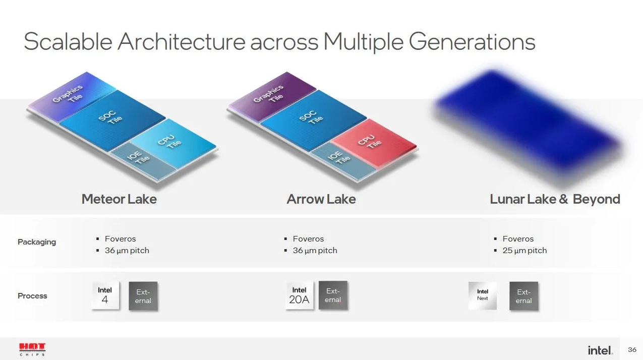
Arrow Lake is Intel’s first desktop chip to use a multi-die configuration. It’s a departure from the outgoing Raptor Lake chips, which used a monolithic setup. Arrow Lake’s chiplet configuration strongly resembles the one used in the company’s last generation Meteor Lake mobile chips. CPU cores sit on a Compute Tile, which is fabricated on a leading edge node. Arrow Lake uses TSMC’s N3B process for the Compute Tile. The iGPU gets its own die, letting Intel scale the GPU without changing the Compute Tile. Because Arrow Lake will likely be paired with a discrete GPU, the iGPU only has four Xe Cores compared to eight on Meteor Lake.
Both the iGPU and CPU dies connect to a central SoC tile, which handles DRAM access and communication with slower IO. The SoC tile also contains a variety of blocks that offer important functionality, but don’t need cutting edge performance to do their job. Arrow Lake’s SoC tile uses TSMC’s cheaper 6 nm node, much like AMD’s IO die. Compared to Meteor Lake’s SoC tile, Arrow Lake ditches the two Crestmont low power E-Cores.
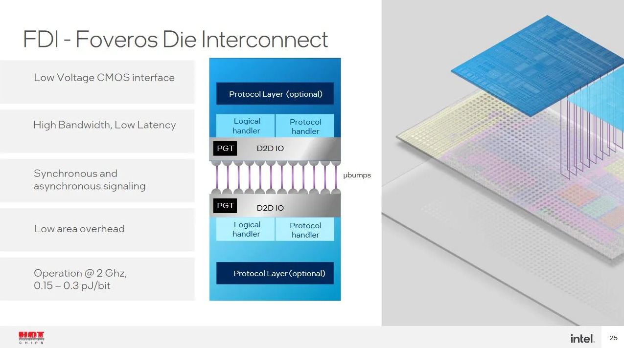
Arrow Lake continues to place tiles on a base die, much like Meteor Lake. Cross-die communication happens through the base tile through Foveros Die Interconnect (FDI) links. That lets Intel achieve very high wire density.
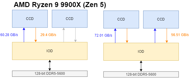
AMD also uses a hub-and-spoke chiplet configuration, and has done so since Zen 2. CPUs are placed on Core Complex Dies (CCDs), which talk to a central IO die. However, AMD’s dies talk to each other through on-package traces. Besides being cheaper, not using a base die or interposer gives AMD’s cross-die links more reach. Being able to place CCDs farther away from the IO die is a notable advantage for server products, where AMD uses many CCDs to hit high core counts.
Flexibility comes with tradeoffs, and AMD’s cross-die links have not kept pace with DDR5 bandwidth. A single CCD has 32 bytes per cycle of read bandwidth and half as much write bandwidth on tap. At AMD’s standard 2 GHz Infinity Fabric clock (FCLK), that’s 64 GB/s of read bandwidth and 32 GB/s of write bandwidth. Fast DDR5 configurations can go well over that, so a bandwidth hungry program can be squeezed by those cross-die links if confined to one CCD.
Arrow Lake’s chiplet setup trades flexibility for higher bandwidth and lower power cross-die links. Intel’s slides at Hot Chips 34 say FDI has ~2K mainband width, and operates at 2 GHz with good power efficiency. Arrow Lake runs the link a bit faster at 2.1 GHz, perhaps improving both bandwidth and latency.
If mainband width refers to data transfer width in bits, then the CPU-SoC link may be capable of moving 2048 bits (256 bytes) per cycle. The resulting 512 GB/s at 2 GHz would be complete overkill even if split for reads and writes. I suspect the data width is less than that, because some pins have to be used for transmitting request addresses, commands, and error correction bits.
In any case, Arrow Lake has plenty of bandwidth between the Compute Tile and the SoC tile. Cross-die bandwidth limitations like those found on AMD chips are completely absent. Read bandwidth on Arrow Lake approaches theoretical DRAM bandwidth. Write bandwidth is somewhat lower, but is still very high and not halved like it is on AMD.
Arrow Lake’s CPU-SoC tile link acts like a better version of Meteor Lake’s. Any set of P-Cores can get full access to DRAM bandwidth. AMD can still achieve high memory bandwidth by using both CCDs together, particularly if using a tuned Infinity Fabric and DRAM setup. But Arrow Lake’s setup is more monolithic with respect to bandwidth behavior.
Latency
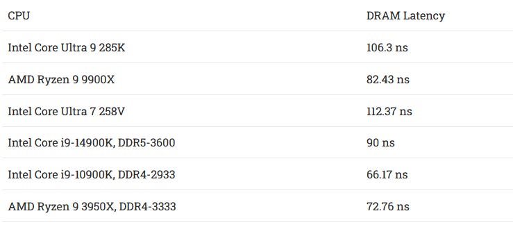
CPU interconnects also need to minimize latency. Arrow Lake’s chiplet set up is less impressive in this regard. Over 100 ns of DRAM load-to-use latency is high for a desktop CPU. Intel didn’t have a problem with DRAM latency in the past. In fact, the outgoing Raptor Lake generation enjoys better DRAM latency, even when running slower DDR5. Past designs show that Intel knows how to make low latency DDR5 controllers. I wonder if Intel’s chiplet setup is to blame.
Latency measurements are complicated by Arrow Lake’s memory controller, which can enter low power modes when bandwidth demands aren’t high enough. However, Arrow Lake appears to snap out of that low power mode if any P-Cores are active. Only E-Cores are affected under low load, which aligns with Arrow Lake’s goals as a performance first design. I got the figures above from a P-Core on Arrow Lake.
High bandwidth load can increase DRAM latency as requests start backing up in various queues throughout the memory subsystem. Bandwidth hungry code can thus affect the performance of latency sensitive code running on other cores. I can investigate these “noisy neighbor” effects by spawning bandwidth-hungry threads while running a latency test thread.

Arrow Lake doesn’t have the CCD-to-IOD pinch points that AMD does. However, Intel’s advantage doesn’t show until I push bandwidth demands past 60 GB/s. Before that point, AMD’s lower baseline latency means it can return data from DRAM faster, even with significant memory traffic. In a previous article, games running on Zen 4 did not get close to demanding 60 GB/s, and average L3 miss latency remained low. Arrow Lake’s high latency, high bandwidth memory subsystem may be well suited to very parallel productivity workloads like image processing. But latency sensitive tasks with low thread counts may not do so well.
Core to Core Latency
A CPU’s memory subsystem also has to give all cores a coherent view of memory, even though each core has its own private caches. If a core reads from an address that has recently been written to by another core, the memory subsystem may have to carry out a cache-to-cache transfer instead of loading data from a shared cache or DRAM. Arrow Lake places all CPU cores within the Compute Tile, so cache-to-cache transfers don’t need to cross die boundaries. Furthermore, Intel has optimized their E-Core clusters to allow cache-to-cache transfers within the same L2 complex. Arrow Lake’s Skymont E-Cores enjoy excellent results in this “core to core” latency test.
Lion Cove P-Cores however don’t do so well. Worst case latency between P-Cores can approach cross-CCD latency on AMD’s chiplet designs. It’s an interesting result considering AMD has to cross two die boundaries to carry out a cache-to-cache transfer across CCDs.
Part of Arrow Lake’s high core-to-core latency may come down to a long ring bus. Each P-Core gets a ring bus stop, as does each quad core E-Core cluster. Add another ring stop for cross-die transfer, and Arrow Lake’s ring bus likely has 13 stops. But latency is worst between Arrow Lake’s P-Cores, so ring bus length is only part of the story.
I suspect Lion Cove’s cache design plays a large role too. Cache coherency protocols ensure only one core can have a particular address cached in modified state. Thus the requesting core in this test will miss in all of its private cache levels. When the core with modified data gets a probe, it has to check all of its own private cache levels, both to read out the modified data and ensure the address is invalidated from its own caches. Lion Cove goes from two levels of core-private data caches to three, adding another step in the process.
A look back at Lunar Lake supports this theory. Lion Cove also sees high core-to-core latency there, even though Lunar Lake’s ring bus only serves four cores. Lunar Lake also displays high cross-cluster latencies, even though those transfers don’t cross die boundaries. How a memory subsystem handles cache coherency operations at the logical level can make a bigger difference than physical die boundaries. and Lunar Lake may be a good example.
Arrow Lake’s Caches: Bigger, Not Always Faster
As a high performance part, Arrow Lake gets more cache capacity for both its P-Cores and E-Cores. DRAM latency has not kept pace with advances in CPU core performance for the past few decades, so caching is crucial to improving CPU performance. With more cache capacity, Arrow Lake’s cores can hopefully spend more of their time carrying out calculations, rather than stalling and waiting for data to come from DRAM.
L3 capacity increases from 12 MB on Lunar Lake to 36 MB on Arrow Lake. Intel has used a L3 cache composed of slices attached to each ring stop since Sandy Bridge, and Arrow Lake has 12 ring stops with cores. That means each slice continues to have 3 MB of capacity like in Lunar Lake. Associativity also stays the same at 12 ways.
Unfortunately, a longer ring bus and higher L3 capacity translate to higher latency. L3 load-to-use latency on Arrow Lake is north of 80 cycles from a P-Core, compared to about 52 cycles on Lunar Lake. The cycle count penalty is high enough that Arrow Lake’s actual L3 latency is higher than Lunar Lake’s, even though Arrow Lake runs at higher clocks.
AMD’s Zen 5 enjoys very low L3 latency, much like prior Zen generations. Each CCX on AMD has 32 MB of L3 cache, giving it comparable capacity to Arrow Lake’s L3. However, AMD uses a separate L3 cache for each CCX. That makes L3 design easier because each L3 instance serves a smaller number of cores. But it’s an inefficient use of SRAM capacity for low threaded workloads, because a single thread can only allocate into 32 MB of L3 cache even though the 9900X has 64 MB of L3 on-chip.
Arrow Lake’s L3 bandwidth improves over Lunar Lake, likely thanks to higher clock speeds at both the core and ring bus. However, bandwidth remains low compare to AMD, as has been the case for several generations. Within Intel’s lineup, a single P-Core’s L3 bandwidth hasn’t improved over what Skylake achieved nine years ago. A Skylake core on the Core i5-6600K could read from L3 at 59.5 GB/s.
L3 bandwidth is more important for multithreaded loads, because one L3 instances serves multiple cores and bandwidth demands scale with active core counts. Usually I test multithreaded bandwidth with each test thread reading from a separate array, which prevents the memory subsystem from combining requests to the same address. However, doing so lets the CPU cache different data in each L2 instance, so I won’t get a good estimate of L3 performance until the amount of test data significantly exceeds total L2 capacity. The Core Ultra 9 285K has 40 MB of L2 and 36 MB of L3. With private arrays per-thread, there’s no amount of test data that’ll fit in L3 without more than half the accesses being served from L2.
To check whether requests were being combined, I monitored Zen 5’s L3 performance events and validated that L3 hit bandwidth closely matched software observations. I couldn’t do the same on Arrow Lake because Intel hasn’t published performance monitoring events yet. But Zen 5’s behavior is a good sign that requests are being combined after L3, not before.
Intel’s L3 performance has lagged behind AMD for a few generations, but Arrow Lake is a notable improvement. Unlike latency, which gets worse with a longer ring bus, L3 bandwidth improves with the number of L3 slices. Different L3 slices can independently handle requests, which can be important if many cores are making requests to L3. Arrow Lake has 12 ring stops compared to eight on Meteor Lake, and runs at higher clocks too. That brings L3 bandwidth to just over 1 TB/s, more than double what Meteor Lake could achieve.
Still, Intel stops short of matching AMD in absolute terms. Even an older 16-core AMD part like the Ryzen 9 3950X enjoys higher L3 bandwidth. The current generation Ryzen 9 9900X pulls ahead of both by a significant margin. Combine that with AMD’s lower latency to L3, and Arrow Lake’s L3 doesn’t look so great. But Intel’s L3 performance needs to be taken with the rest of the cache hierarchy in perspective. Arrow Lake’s P-Cores see their L2 capacity bumped to 3 MB, while E-Core clusters keep the same large 4 MB L2 they had in Lunar Lake. AMD in contrast uses smaller 1 MB L2 caches, because the cost of a L2 miss is lower.
Arrow Lake should also be seen with Lunar Lake in perspective. Skymont cores on Lunar Lake sat on a low power island away from the ring bus, and saw high L2 miss latency even if the request was serviced from Lunar Lake’s 8 MB memory side cache. Arrow Lake doesn’t need E-Cores to reduce power during low intensity tasks, and focuses on using them to boost multithreaded performance. To that end, Skymont clusters go back to sitting on the ring bus like standard E-Cores from prior generations. Having a L3, even a slow one, is worlds better than nothing at all.
Overall, Arrow Lake largely carries forward the caching strategy used in prior generations. Raptor Lake and Alder Lake before had lackluster L3 performance, but compensated with larger L2 caches than their AMD counterparts. Intel also has larger cores that can speculate further ahead of a stalled instruction, putting them in a better spot to maintain decent throughput in the face of long load latency. AMD isn’t too different in that regard. Zen 4 doubled L2 capacity to 1 MB, significantly reducing average L3 traffic in the process. Recent Arm server chips also use large (1 or 2 MB) L2 caches to mitigate L3 latency. Thus other CPU makers are also taking advantage of process node improvements to keep more data closer to their cores. Arrow Lake does lean a bit harder on L2 capacity than other architectures, because it needs to deliver high per-core performance while using a relatively slower L3.
Clock Speed
Clock speed continues to be an important lever for improving CPU performance, alongside architectural changes that boost performance per clock. Arrow Lake’s Lion Cove and Skymont cores both clock higher than they do in Lunar Lake, which is to be expected for a higher power, higher performance design. Two of the Core Ultra 9 285K’s Lion Cove cores can reach 5.7 GHz. The rest can hit 5.5 GHz. All of the Skymont E-Cores run at up to 4.6 GHz.
Skymont’s clock speed deserves special attention because it’s quite high in an absolute sense, even if it doesn’t match current generation desktop P-Core clocks. Just a few years ago, AMD’s Zen 2 topped out at 4.7 GHz, but couldn’t do so across every core. Intel’s E-Cores have a trend of catching prior generation P-Cores in some areas, and clock speed is another such area with Skymont.
Compared to Arrow Lake, AMD’s Ryzen 9 9900X has very uniform clock speeds within a CCD. All cores on the first CCD can run at 5.6 GHz, while all cores on the second CCD run at 5.35 GHz. Arrow Lake can clock higher at 5.7 GHz if you pick the right core, but AMD and Intel are running their high performance cores at very similar clocks this generation. Even though more of AMD’s cores can reach the highest clock speeds, operating systems will have to categorize cores by their expected performance class to optimize low threaded workloads.
Final Words
Intel has been busy shaking up their lineup from top to bottom over the past few years. The large monolithic dies that characterized Intel’s glory days of the early 2010s are gone in favor of more flexible chiplet designs. Just as Meteor Lake brought chiplets into Intel’s laptop offerings, Arrow Lake does the same on desktop. Both Intel client chips use a hub-and-spoke chiplet topology like AMD. And both companies can select the most appropriate node for each die. Past that though, AMD and Intel’s chiplet strategies differ.
Intel still focuses on building a monolithic-feeling design. That has advantages like more uniform bandwidth characteristics, or keeping cache-to-cache transfers within the same die. But challenges often accompany change. Arrow Lake regresses DRAM latency, an important metric if application working sets spill out of cache. Change also consumes engineering time, and using engineering time on one thing is an opportunity cost. Intel likely didn’t have engineering time left to improve other aspects like L3 performance or capacity.
Hopefully as Intel gets more experience deploying chiplets across different market segments, they’ll start to reap the benefits of chiplet reuse and process node flexibility. And with the difficult initial chiplet design work out of the way after Meteor Lake and Arrow Lake, perhaps Intel will find they have engineering bandwidth available to address L3 and DRAM latency. If they can pull that off, Intel’s huge out-of-order execution engines can shine.
If you like our articles and journalism, and you want to support us in our endeavors, then consider heading over to our Patreon or our PayPal if you want to toss a few bucks our way. If you would like to talk with the Chips and Cheese staff and the people behind the scenes, then consider joining our Discord.


285k doubled p-core core-to-core latency when comparing to 14900k, which also has 12 L3 slices.
285k L3 latency is similar to 14900k, but loses to 14900k over a variety of worklords.
It'd be great if you could further examine it when intel rolls out all 'fixes' and PMU events are published.
So ever since Intel moved to non-inclusive cache design, their strategy is to emphasize the private caches at the expense of the L3, while AMD's huge and fast L3 cache and relatively modest private caches strategy seems to gain more net performance.