
Blackwell: Nvidia’s Massive GPU

Nvidia has a long tradition of building giant GPUs. Blackwell, their latest graphics architecture, continues that tradition. GB202 is the largest Blackwell die. It occupies a massive 750mm2 of area, and has 92.2 billion transistors. GB202 has 192 Streaming Multiprocessors (SMs), the closest equivalent to a CPU core on a GPU, and feeds them with a massive memory subsystem. Nvidia’s RTX PRO 6000 Blackwell features the largest GB202 configuration to date. It sits alongside the RTX 5090 in Nvidia’s lineup, which also uses GB202 but disables a few more SMs.
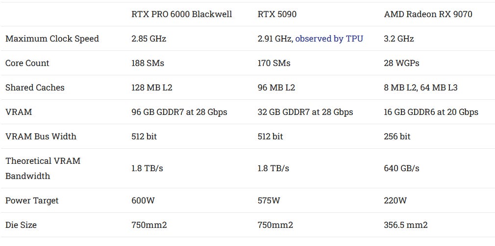
A high level comparison shows the scale of Nvidia’s largest Blackwell products. AMD’s RDNA4 line tops out with the RX 9070 and RX 9070XT. The RX 9070 is slightly cut down, with four WGPs disabled out of 32. I’ll be using the RX 9070 to provide comparison data.
Acknowledgement
A massive thanks to Will Killian for giving us access to his RTX PRO 6000 Blackwell system for us to test. And so, a massive thanks goes out to him for this article!
Work Distribution
GPUs use specialized hardware to launch threads across their cores, unlike CPUs that rely on software scheduling in the operating system. Hardware thread launch is well suited to the short and simple tasks that often characterize GPU workloads. Streaming Multiprocessors (SMs) are the basic building block of Nvidia GPUs, and are roughly analogous to a CPU core. SMs are grouped into Graphics Processing Clusters (GPCs), which contain a rasterizer and associated work distribution hardware.

GB202 has a 1:16 GPC to SM ratio, compared to the 1:12 ratio found in Ada Lovelace’s largest AD102 die. That lets Nvidia cheaply increase SM count and thus compute throughput without needing more copies of GPC-level hardware. However, dispatches with short-duration waves may struggle to take advantage of Blackwell’s scale, as throughput becomes limited by how fast the GPC can allocate work to the SMs rather than how fast the SMs can finish them.
AMD’s RDNA4 uses a 1:8 SE:WGP ratio, so one rasterizer feeds a set of eight WGPs in a Shader Engine. WGPs on AMD are the closest equivalent to SMs on Nvidia, and have the same nominal vector lane count. RDNA4 will be easier to utilize with small dispatches and short duration waves, but it’s worth noting that Blackwell’s design is not out of the ordinary. Scaling up GPU “cores” independently of work distribution hardware is a common technique for building larger GPUs. AMD’s RX 6900XT (RDNA2) had a 1:10 SE:WGP ratio. Before that, AMD’s largest GCN implementations like Fury X and Vega 64 had a 1:16 SE:CU ratio (CUs, or Compute Units, formed the basic building block of GCN GPUs). While Blackwell does have the same ratio as those large GCN parts, it enjoys higher clock speeds and likely has a higher wave launch rate to match per-GPU-core throughput. It won’t suffer as much as the Fury X from 10 years ago with short duration waves, but GB202 will still be harder to feed than smaller GPUs.

Although Nvidia didn’t scale up work distribution hardware, they did make improvements on Blackwell. Prior Nvidia generations could not overlap workloads of different types on the same queue. Going between graphics and compute tasks would require a “subchannel switch” and a “wait-for-idle”. That requires one task on the queue to completely finish before the next can start, even if a game doesn’t ask for synchronization. Likely, higher level scheduling hardware that manages queues exposed to host-side applications can only track state for one workload type at a time. Blackwell does away with subchannel switches, letting it more efficiently fill its shader array if applications frequently mix different work types on the same queue.
SM Frontend
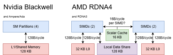
Once assigned work, the SM’s frontend fetches shader program instructions and delivers them to the execution units. Blackwell uses fixed length 128-bit (16 byte) instructions, and the SM uses a two-level instruction caching setup. Both characteristics are carried forward from Nvidia’s post-Turing/Volta designs. Each of the SM’s four partitions has a private L0 instruction cache, while a L1 instruction cache is shared across the SM.

Nvidia’s long 16 byte instructions translate to high instruction-side bandwidth demands. The L0+L1 instruction caching setup is likely intended to handle those bandwidth demands while also maintaining performance with larger code footprints. Each L0 only needs to provide one instruction per cycle, and its smaller size should make it easier to optimize for high bandwidth and low power. The SM-level L1 can then be optimized for capacity.
Blackwell’s L1i is likely 128 KB, from testing with unrolled loops of varying sizes and checking generated assembly (SASS) to verify the loop’s footprint. The L1i is good for approximately 8K instructions, providing a good boost over prior Nvidia generations.
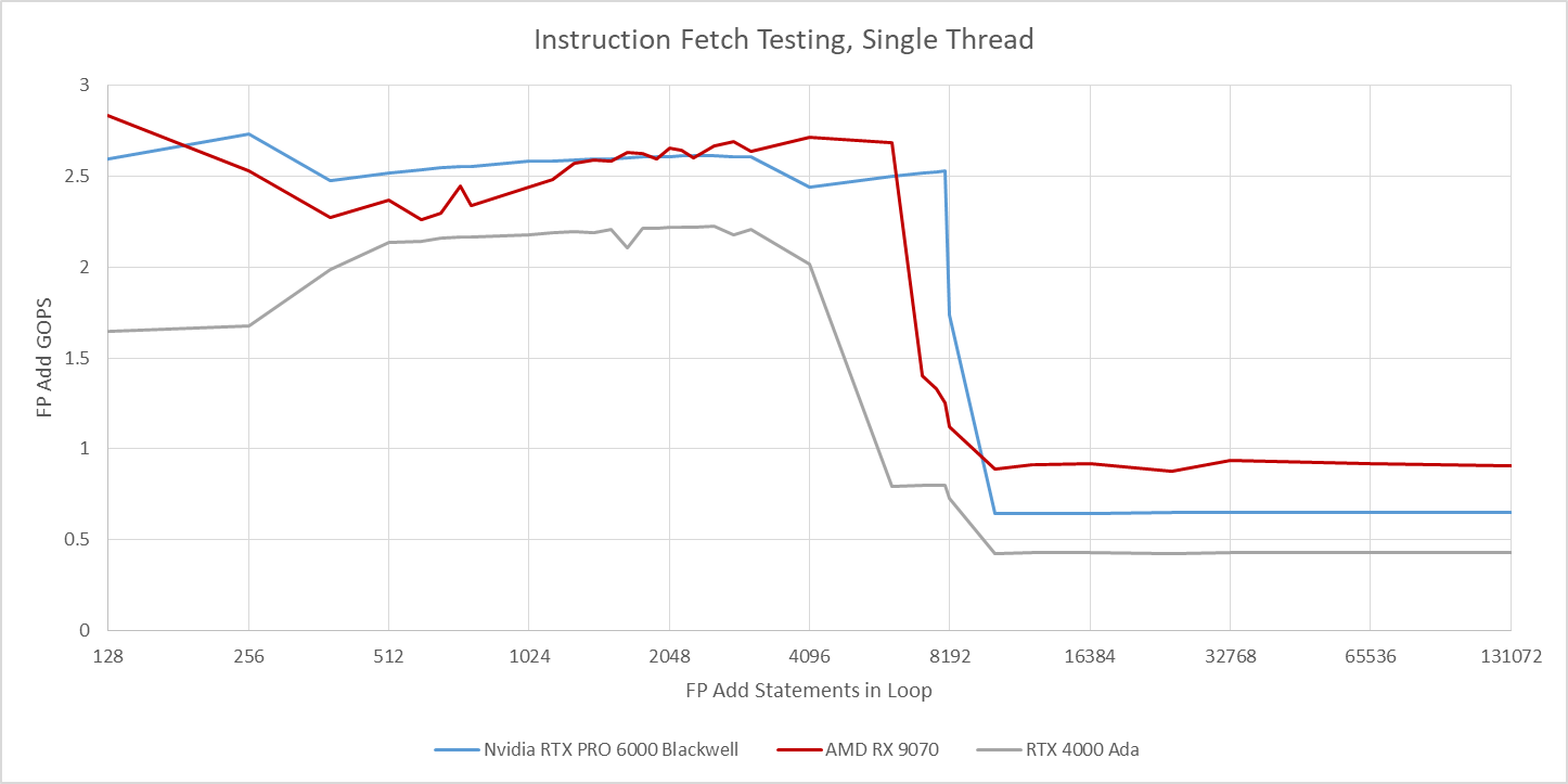
Blackwell and Ada Lovelace both appear to have 32 KB L0i caches, which is an increase over 16 KB in Turing. The L1i can fully feed a single partition, and can filter out redundant instruction fetches to feed all four partitions. However, L1i bandwidth can be a visible limitation if two waves on different partitions spill out of L1i and run different code sections. In that case, per-wave throughput drops to one instruction per two cycles.

AMD uses variable length instructions ranging from 4 to 12 bytes, which lowers capacity and bandwidth pressure on the instruction cache compared to Nvidia. RDNA4 has a 32 KB instruction cache shared across a Workgroup Processor (WGP), much like prior RDNA generations. Like Nvidia’s SM, a WGP is divided into four partitions (SIMDs). RDNA1’s whitepaper suggests the L1i can supply 32 bytes per cycle to each SIMD. It’s an enormous amount of bandwidth considering AMD’s more compact instructions. Perhaps AMD wanted to be sure each SIMD could co-issue to its vector and scalar units in a sustained fashion. In this basic test, RDNA4’s L1i has no trouble maintaining full throughput when two waves traverse different code paths. RDNA4 also enjoys better code read bandwidth from L2, though all GPUs I’ve tested show poor L2 code read bandwidth.
Execution Units
Each Blackwell SM partition can track up to 12 waves to hide latency, which is a bit lower than the 16 waves per SIMD on RDNA4. Actual occupancy, or the number of active wave slots, can be limited by a number of factors including register file capacity. Nvidia has not changed theoretical occupancy or register file capacity since Ampere, and the latter remains a 64 KB per partition. A kernel therefore can’t use more than 40 registers while using all 12 wave slots, assuming allocation granularity hasn’t changed since Ada and is still 8 registers. For comparison, AMD’s high end RDNA3/4 SIMDs have 192 KB vector register files, letting a kernel use up to 96 registers while maintaining maximum occupancy.

Blackwell’s primary FP32 and INT32 execution pipelines have been reorganized compared to prior generations, and are internally arranged as one 32-wide execution pipe. That creates similarities to AMD’s RDNA GPUs, as well as Nvidia’s older Pascal. Having one 32-wide pipe handle both INT32 and FP32 means Blackwell won’t have to stall if it encounters a long stream of operations of the same type. Blackwell inherits Turing’s strength of being able to do 16 INT32 multiplies per cycle in each partition. Pascal and RDNA GPUs can only do INT32 multiplies at approximately quarter arte (8 per partition, per cycle).

Compared to Blackwell, AMD’s RDNA4 packs a lot of vector compute into each SIMD. Like RDNA3, RDNA4 can use VOPD dual issue instructions or wave64 mode to complete 64 FP32 operations per cycle in each partition. An AMD SIMD can also co-issue instructions of different types from different waves, while Nvidia’s dispatch unit is limited to one instruction per cycle. RDNA4’s SIMD also packs eight special function units (SFUs) compared to four on Nvidia. These units handle more complex operations like inverse square roots and trigonometric functions.

Differences in per-partition execution unit layout or count quickly get pushed aside by Blackwell’s massive SM count. Even when the RX 9070 can take advantage of dual issue, 28 WGPs cannot take on 188 SMs. Nvidia holds a large lead in every category.
Other SM-Level Changes
Nvidia added floating point instructions to Blackwell’s uniform datapath, which dates back to Turing and serves a similar role to AMD’s scalar unit. Both offload instructions that are constant across a wave. Blackwell’s uniform FP instructions include adds, multiples, FMAs, min/max, and conversions between integer and floating point. Nvidia’s move mirrors AMD’s addition of FP scalar instructions with RDNA 3.5 and RDNA4.
Still, Nvidia’s uniform datapath feels limited compared to AMD’s scalar unit. Uniform registers can only be loaded from constant memory, though curiously a uniform register can be written out to global memory. I wasn’t able to get Nvidia’s compiler to emit uniform instructions for the critical part of any instruction or cache latency tests, even when loading values from constant memory.
Raytracing has long been a focus of Nvidia’s GPUs. Blackwell doubles the per-SM ray triangle intersection test rate, though Nvidia does not specify what the box or triangle test rate is. Like Ada Lovelace, Blackwell’s raytracing hardware supports “Opacity Micromaps”, providing functionality similar to the sub-triangle opacity culling referenced by Intel’s upcoming Xe3 architecture.
SM Memory Subsystem
Like Ada Lovelace and Ampere, Blackwell has a SM-wide 128 KB block of storage that’s partitioned for use as L1 cache and Shared Memory. Shared Memory is Nvidia’s term for a software managed scratchpad, which backs the local memory space in OpenCL. AMD’s equivalent is the Local Data Share (LDS), and Intel’s is Shared Local Memory (SLM). Unlike with their datacenter GPUs, Nvidia has chosen not to increase L1/Shared Memory capacity. As in prior generations, different L1/Shared Memory splits do not affect L1 latency.

AMD’s WGPs use a more complex memory subsystem, with a high level design that debuted in the first RDNA generation. The WGP has a 128 KB LDS that’s internally built from a pair of 64 KB, 32-bank structures connected by a crossbar. First level vector data caches, called L0 caches, are private to pairs of SIMDs. A WGP-wide 16 KB scalar cache services scalar and constant reads. In total, a RDNA4 WGP has 208 KB of data-side storage divided across different purposes.
A RDNA4 WGP enjoys substantially higher bandwidth from its private memories for global and local memory accesses. Each L0 vector cache can deliver 128 bytes per cycle, and the LDS can deliver 256 bytes per cycle total to the WGP. Mixing local and global memory traffic can further increase achievable bandwidth, suggesting the LDS and L0 vector caches have separate data buses.

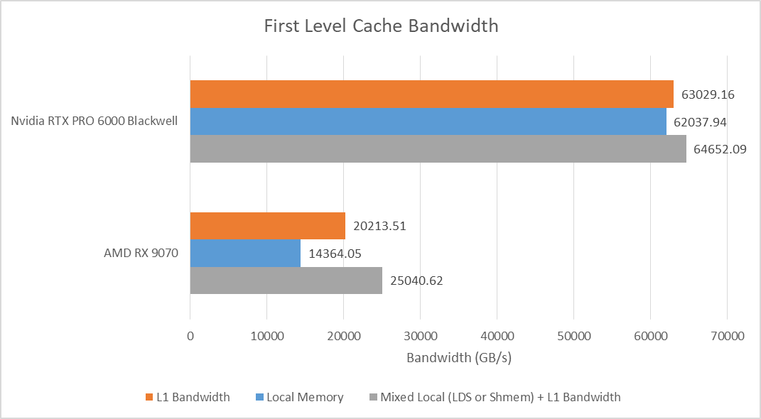
Doing the same on Nvidia does not bring per-SM throughput past 128B/cycle, suggesting the 128 KB L1/Shared Memory block has a single 128B path to the execution units.

Yet any advantage AMD may enjoy from this characteristic is blunted as the RX 9070 drops clocks to 2.6 GHz, in order to stay within its 220W power target. Nvidia in contrast has a higher 600W power limit, and can maintain close to maximum clock speeds while delivering 128B/cycle from SM-private L1/Shared Memory storage.
Just as with compute, Nvidia’s massive scale pushes aside any core-for-core differences. The 188 SMs across the RTX PRO 6000 Blackwell together have more than 60 TB/s of bandwidth. High SM count gives Nvidia more total L1/local memory too. Nvidia has 24 MB of L1/Shared Memory across the RTX PRO 6000. AMD’s RX 9070 has just under 6 MB of first level data storage in its WGPs.
SM-private storage typically offers low latency, at least in GPU terms, and that continues to be the case in Blackwell. Blackwell compares favorably to AMD in several areas, and part of that advantage comes down to address generation. I’m testing with dependent array accesses, and Nvidia can convert an array index to an address with a single IMAD.WIDE instruction.

AMD has fast 64-bit address generation through its scalar unit, but of course can only use that if the compiler determines the address calculation will be constant across a wave. If each lane needs to independently generate its own address, AMD’s vector integer units only natively operate with 32-bit data types and must do an add-with-carry to generate a 64-bit address.

Because separating address generation from cache latency is impossible, Nvidia enjoys better L1 vector access latency. AMD can be slightly faster if the compiler can carry out scalar optimizations.

GPUs can also offload address generation to the texture unit, which can handle an array address calculations. The texture unit of course can also do texture filtering, though I’m only asking it to return raw data when testing with OpenCL’s image1d_buffer_t type. AMD enjoys lower latency if the texture unit does address calculations, but Nvidia does not.
Atomics
GPUs often handle atomic operations with dedicated ALUs placed close to points of coherency, like the LDS or Shared Memory for local memory, or the L2 cache for global memory. That contrasts with CPUs, which rely on locking cachelines to handle atomics and ensure ordering. Nvidia appears to have 16 INT32 atomic ALUs at each SM, compared to 32 for each AMD WGP.

In a familiar trend, Nvidia can crush AMD by virtue of having a much bigger GPU, at least with local memory atomics. Both the RTX PRO 6000 and RX 9070 have surprisingly similar atomic add throughput in global memory, suggesting Nvidia either has fewer L2 banks or fewer atomic units per bank.

RDNA4 and Blackwell have similar latency when threads exchange data through atomic compare and exchange operations, though AMD is slightly faster. The RX 9070 is a much smaller and higher clocked GPU, and both can help lower latency when moving data across the GPU.

GPU-Wide Memory Subsystem
Blackwell uses a conventional two-level data caching setup, but continues Ada Lovelace’s strategy of increasing L2 capacity to achieve the same goals as AMD’s Infinity Cache. L2 latency on Blackwell regresses to just over 130 ns, compared to 107 ns on Ada Lovelace. Nvidia’s L2 latency continues to sit between AMD’s L2 and Infinity Cache latencies, though now it’s noticeably closer to the latter.

Tests results using Vulkan suggest the smaller RTX 5070 also has higher L2 latency (122 ns) than the RTX 4090, even though the 5070 has fewer SMs and a smaller L2. Cache latency results from Nemes’s Vulkan test suite should be broadly comparable to my OpenCL ones, because we both use a current = arr[current] access pattern. A deeper look showed minor code generation differences that seem to add ~3 ns of latency to the Vulkan results. That doesn’t change the big picture with L2 latencies. Furthermore, the difference between L1 and L2 latency should approximate the time taken to traverse the on-chip network and access the L2. Differences between OpenCL and Vulkan results are insignificant in that regard. Part of GB202’s L2 latency regression may come from its massive scale, but results from the 5070 suggest there’s more to the picture.

The RTX PRO 6000 Blackwell’s VRAM latency is manageable at 329 ns, or ~200 ns over L2 hit latency. AMD’s RDNA4 manages better VRAM latency at 254 ns for a vector access, or 229 ns through the scalar path. Curiously, Nvidia’s prior Ada Lovelace and Ampere architectures enjoyed better VRAM latency than Blackwell, and are in the same ballpark as RDNA4 and RDNA2.
Blackwell’s L2 bandwidth is approximately 8.7 TB/s, slightly more than the RX 9070’s 8.4 TB/s. Nvidia retains a huge advantage at larger test sizes, where AMD’s Infinity Cache provides less than half the bandwidth. In VRAM, Blackwell’s GDDR7 and 512-bit memory bus continue to keep it well ahead of AMD.

Nvidia’s L2 performance deserves closer attention, because it’s one area where the RX 9070 gets surprisingly close to the giant RTX PRO 6000 Blackwell. A look at GB202’s die photo shows 64 cache blocks, suggesting the L2 is split into 64 banks. If so, each bank likely delivers 64 bytes per cycle (of which the test was able to achieve 48B/cycle). It’s an increase over the 48 L2 blocks in Ada Lovelace’s largest AD102 chip. However, Nvidia's L2 continues to have a tough job serving as both the first stop for L1 misses and as a large last level cache. In other words, it’s doing the job of AMD’s L2 and Infinity Cache levels. There’s definitely merit to cutting down cache levels, because checking a level of cache can add latency and power costs. However, caches also have to make a tradeoff between capacity, performance, and power/area cost.

Nvidia likely relies on their flexible L1/Shared Memory arrangement to keep L2 bandwidth demands under control, and insulate SMs from L2 latency. A Blackwell SM can use its entire 128 KB L1/Shared Memory block as L1 cache if a kernel doesn’t need local memory, while an AMD WGP is stuck with two 32 KB vector caches and a 16 KB scalar cache. However a kernel bound by local memory capacity with a data footprint in the range of several megabytes would put Nvidia at a disadvantage. Watching AMD and Nvidia juggle these tradeoffs is quite fun, though it’s impossible to draw any conclusions with the two products competing in such different market segments.
Compute Performance: FluidX3D
FluidX3D simulates fluid behavior and can demand plenty of memory bandwidth. It carries out computations with FP32 values, but can convert them to FP16 formats for storage. Doing so reduces VRAM bandwidth and capacity requirements. Nvidia’s RTX PRO 6000 takes a hefty lead over AMD’s RX 9070, as the headline compute and memory bandwidth specifications would suggest.

Nvidia’s lead remains relatively constant regardless of what mode FluidX3D is compiled with.
Final Words
We technically have more GPU competition than ever in 2025, as Intel’s GPU effort makes steady progress and introduces them as a third contender. On the datacenter side, AMD’s MI300 has proven to be very competitive with supercomputing wins. But competition is conspicuously absent at the top of the consumer segment. Intel’s Battlemage and AMD’s RDNA4 stop at the midrange segment. The RX 9070 does target higher performance levels than Intel’s Arc B580, but neither come anywhere close to Nvidia’s largest GB202 GPUs.
As for GB202, it’s yet another example of Nvidia building as big as they can to conquer the top end. The 750mm2 die pushes the limits of what can be done with a monolithic design. Its 575W or 600W power target tests the limits of what a consumer PC can support. By pushing these limits, Nvidia has created the largest consumer GPU available today. The RTX PRO 6000 incredibly comes close to AMD’s MI300X in terms of vector FP32 throughput, and is far ahead of Nvidia’s own B200 datacenter GPU. The memory subsystem is a monster as well. Perhaps Nvidia’s engineers asked whether they should emphasize caching like AMD’s RDNA2, or lean on VRAM bandwidth like they did with Ampere. Apparently, the answer is both. The same approach applies to compute, where the answer was apparently “all the SMs”.
Building such a big GPU isn’t easy, and Nvidia evidently faced their share of challenges. L2 performance is mediocre considering the massive compute throughput it may have to feed. Beyond GPU size, comparing with RDNA4 shows continued trends like AMD using a smaller number of individually stronger cores. RDNA4’s basic Workgroup Processor building block has more compute throughput and cache bandwidth than a Blackwell SM.
But none of that matters at the top end, because Nvidia shows up with over 6 times as many “cores”, twice as much last level cache capacity, and a huge VRAM bandwidth lead. Some aspects of Blackwell may not have scaled as nicely. But Nvidia’s engineers deserve praise because everyone else apparently looked at those challenges and decided they weren’t going to tackle them at all. Blackwell therefore wins the top end by default. Products like the RTX PRO 6000 are fascinating, and I expect Nvidia to keep pushing the limits of how big they can build a consumer GPU. But I also hope competition at the top end will eventually reappear in the decades and centuries to come.
If you like the content then consider heading over to the Patreon or PayPal if you want to toss a few bucks to Chips and Cheese. Also consider joining the Discord.
References
SASS instruction listings: https://docs.nvidia.com/cuda/cuda-binary-utilities/index.html#blackwell-instruction-set
GB202 whitepaper: https://images.nvidia.com/aem-dam/Solutions/geforce/blackwell/nvidia-rtx-blackwell-gpu-architecture.pdf
Blackwell PRO GPU whitepaper: https://www.nvidia.com/content/dam/en-zz/Solutions/design-visualization/quadro-product-literature/NVIDIA-RTX-Blackwell-PRO-GPU-Architecture-v1.0.pdf
Techpowerup observing that the RTX 5090 could reach 2.91 GHz: https://www.techpowerup.com/review/nvidia-geforce-rtx-5090-founders-edition/44.html
Thank you for your insightful post, as always!
As indicated in the PTX documentation (https://docs.nvidia.com/cuda/parallel-thread-execution/#integer-arithmetic-instructions-mad ), IMAD and IMAD.WIDE means 32-bit × 32-bit → 32-bit/64-bit integer multiplication, resp.
According to Table 7 in https://docs.nvidia.com/cuda/cuda-c-programming-guide/index.html#arithmetic-instructions , widening multiplication delivers only half the throughput of its non-widening counterpart, so the compiler appears to favor non-widening one for 32-bit address generation for shared space.
Also, thanks to @Chester for another great deep dive!