
Arm’s Cortex A725 ft. Dell’s Pro Max with GB10

Arm’s 7-series cores started out as the company’s highest performance offerings. After Arm introduced the performance oriented X-series, 7-series cores have increasingly moved into a density focused role. Like Intel’s E-Cores, Arm’s 7-series cores today derive their strength from numbers. A hybrid core setup can ideally use density-optimized cores to achieve high multithreaded performance at lower power and area costs than a uniform big-core design. The Cortex A725 is the latest in Arm’s 7-series, and arrives when Arm definitely wants a strong density optimized core. Arm would like SoC makers to license their cores rather than make their own. Arm probably hopes their big+little combination can compare well with Qualcomm’s custom cores. Beyond that, Arm’s efforts to expand into the x86-64 dominated laptop segment would benefit from a good density optimized core too.
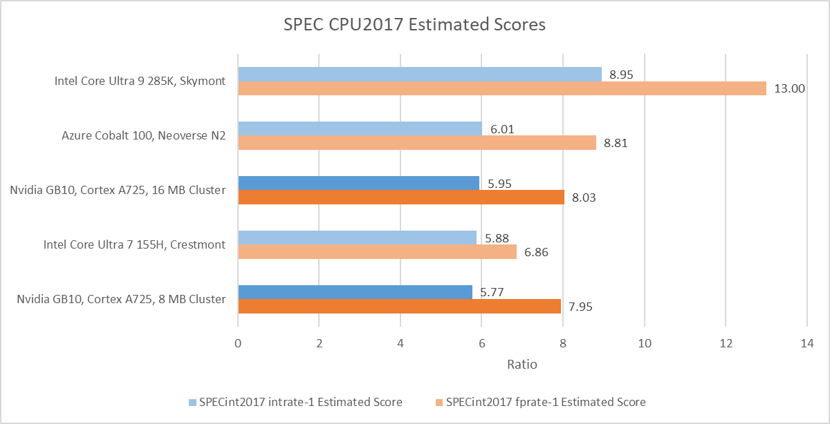
Here, I’ll be looking into the Cortex A725 in Nvidia’s GB10. GB10 has ten A725 cores and ten X925 cores split across two clusters, with five of each core type in each. The A725 cores run at 2.8 GHz, while the high performance X925 cores reach 3.9 to 4 GHz. As covered before, one of GB10’s clusters has 8 MB of L3, while the other has 16 MB. GB10 will provide a look at A725’s core architecture, though implementation choices will obviously influence performance. For comparison, I’ll use older cores from Arm’s 7-series line as well as Intel’s recent Skymont E-Core.
Acknowledgements
A massive thanks to Dell for sending over two of their Pro Max with GB10 for testing. In our testing the Dell Pro Maxs were quite quiet even when under a Linpack load which speaks to Dell’s thermal design keeping the GB10 SoC within reasonable levels.
Overview
Cortex A725 is a 5-wide out-of-order core with reordering capacity roughly on par with Intel’s Skylake or AMD’s Zen 2. Its execution engine is therefore large enough to dip deep into the benefits of out-of-order execution, but stops well short of high performance core territory. The core connects to the rest of the system via Arm’s DynamIQ Shared Unit 120 (DSU-120) via 256-bit read and write paths. Arm’s DSU-120 acts as a cluster level interconnect and contains the shared L3 cache.
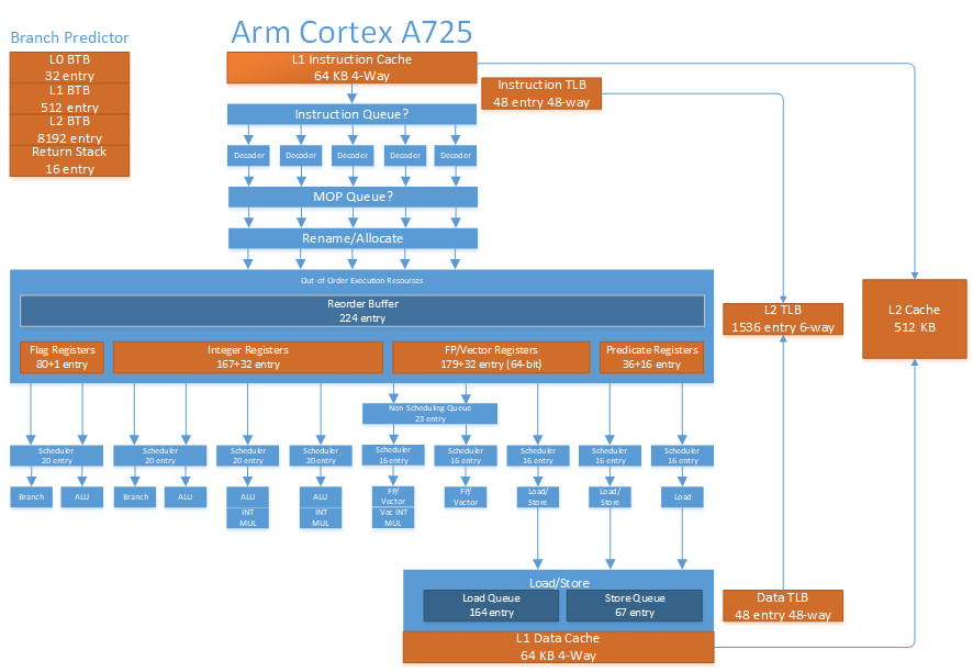
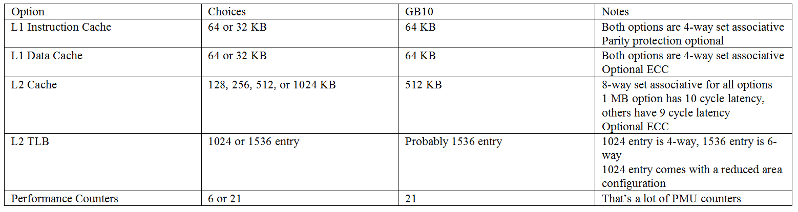
In Arm tradition, A725 offers a number of configuration options to let implementers fine tune area, power, and performance. These options include:
Branch Predictor
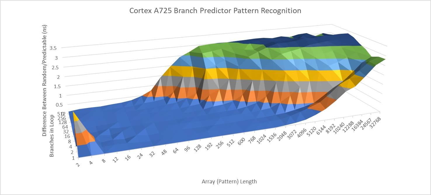
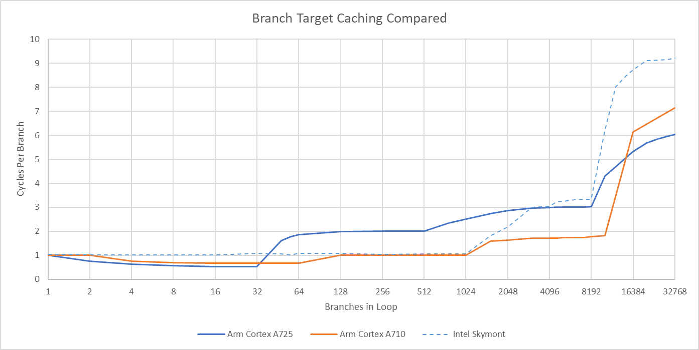
Cortex A710’s branch predictor already showed capabilities on par with older Intel high performance cores, and A725 inherits that strength. In a test where branch direction correlates with increasingly long random patterns, A725 trades blows with A715 rather than being an overall improvement. With a single branch, latencies start going up once the random pattern exceeds 2048 for a single branch, versus 3072 on A710. With 512 branches in play, both A710 and A725 see higher latencies once the pattern length exceeds 32. However, A725 shows a gradual degradation compared to the abrupt one seen on A710.

Arm’s 7-series cores historically used branch target buffers (BTBs) with very low cycle count latencies, which helped make up for their low clock speed. A725’s BTB setup is fine on its own, but regresses compared to A710. Each BTB level is smaller compared to A710, and the larger BTB levels are slower too.
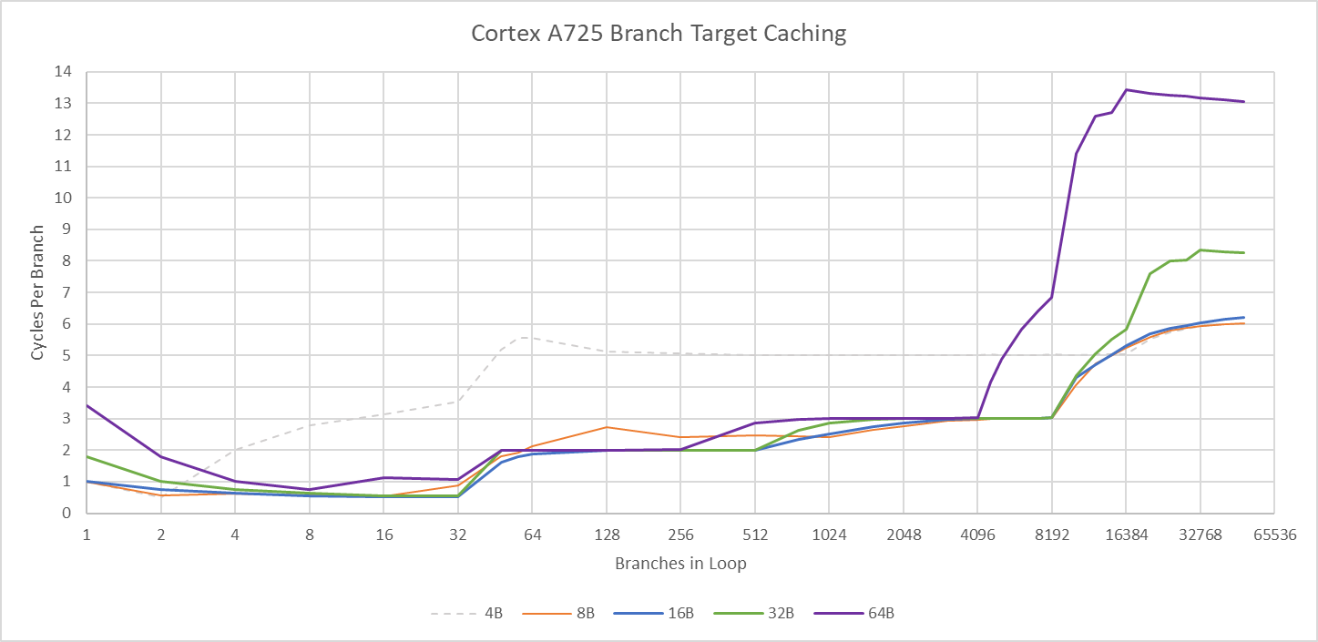
A725’s taken branch performance trades blows with Skymont. Tiny loops favor A725, because Skymont can’t do two taken branches per cycle. Moderate branch counts give Skymont a win, because Intel’s 1024 entry L1 BTB has single cycle latency. Getting a target out of A725’s 512 entry L1 BTB adds a pipeline bubble. Then, both cores have similar cycle count latencies to a 8192 entry L2 BTB. However, that favors Skymont because of its higher clock speed.
Returns, or branch-with-link instructions in Arm terms, are predicted on A725 using a 16 entry return stack. A call+return pair has a latency of two cycles, so each branch likely executes with single cycle latency.
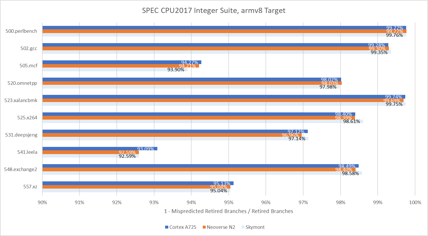
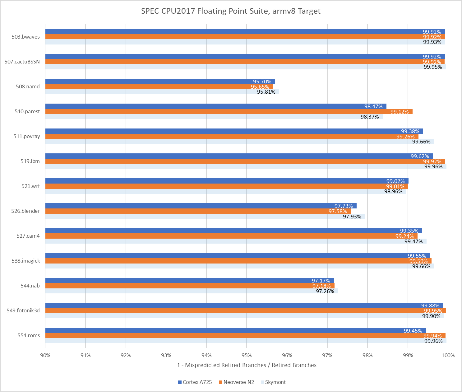
In SPEC CPU2017, A725 holds the line in workloads that are easy on the branch predictor while sometimes delivering improvements in difficult tests. 541.leela is the most impressive case. In that workload. A725 manages a 6.61% decrease in mispredicts per instruction compared to Neoverse N2. Neoverse N2 is a close relative of Cortex A710, and was tested here in Azure’s Cobalt 100. A725’s gains are less clear in SPEC CPU2017’s floating point workloads, where it trades blows with Neoverse N2. Still, it’s an overall win for A725 because SPEC’s floating point workloads are less branchy and put more emphasis on core throughput.
Comparing with Skymont is more difficult because there’s no way to match the instruction stream due to ISA differences. It’s safe to say the two cores land in the same ballpark, and both have excellent branch predictors.
Instruction Fetch and Decode
After the branch predictor has decided where to go, the frontend has to fetch instructions and decode them into the core’s internal format. Arm’s cores decode instructions into macro-operations (MOPs), which can be split further into micro-operations (uOPs) in later pipeline stages. Older Arm cores could cache MOPs in a MOP cache, much like AMD and Intel’s high performance CPUs. A725 drops the MOP cache and relies exclusively on a conventional fetch and decode path for instruction delivery. The fetch and decode path can deliver 5 MOPs per cycle, which can correspond to 6 instructions if the frontend can fuse a pair of instructions into a single MOP. With a stream of NOPs, A725’s frontend delivers five instructions per cycle until test sizes spill out of the 32 entry instruction TLB. Frontend bandwidth then drops to under 2 IPC, and stays there until the test spills out of L3.
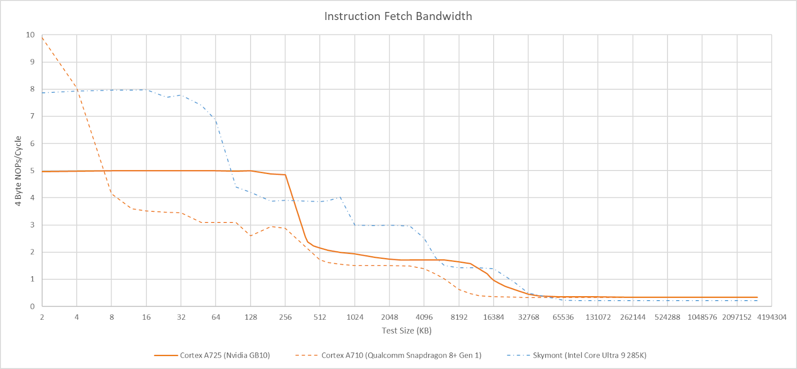
For comparison, A710 could use its MOP cache to hit 10 IPC if each MOP corresponds to a fused instruction pair. That’s easy to see with a stream of NOPs, because A710 can fuse pairs of NOPs into a single MOP. A725’s decoders can no longer fuse pairs of adjacent NOPs, though they still support other fusion cases like CMP+branch.
Arm’s decision to ditch the MOP cache deserves discussion. I think it was long overdue, because Arm cores already took plenty of measures to mitigate decode costs. Chief among these is a predecode scheme. Instructions are partially decoded when they’re filled into the instruction cache. L1I caches on cores up to the Cortex A78 and Cortex X1 stored instructions in a 36 or 40-bit intermediate format. It’s a compromise between area-hungry micro-op caching and fully decoding instructions with every fetch. Combining predecode and micro-op caching is overkill, especially on low clocked cores where timing should be easier. Seeing A710 hit ridiculous throughput in an instruction bandwidth microbenchmark was fun, but it’s a corner case. Arm likely determined that the core rarely encountered more than one instruction fusion candidate per cycle, and I suspect they’re right.
A725’s Technical Reference Manual suggests Arm uses a different predecode scheme now, with 5 bits of “sideband” predecode data stored alongside each 32-bit aarch64 instruction. Sideband bit patterns indicate a valid opcode. Older Arm CPUs used the intermediate format to deal with the large and non-contiguous undefined instruction space. A725’s sideband bits likely cover the same purpose, along with aiding the decoders for valid instructions.
Rename and Allocate
MOPs from the frontend go to the rename/allocate stage, which can handle five MOPs per cycle. Besides doing classical register renaming to remove false dependencies, modern CPUs can pull a variety of tricks to expose additional parallelism. A725 can recognize moving an immediate value of 0 to a register as a zeroing idiom, and doesn’t need to allocate a physical register to hold that instruction’s result. Move elimination is supported too, though A725 can’t eliminate chained MOVs across all renamer slots like AMD and Intel’s recent cores. In a test with independent MOVs, A725 allocates a physical register for every instruction. Arm’s move elimination possibly fails if the renamer encounters too many MOVs in the same cycle. That’s what happens on Intel’s Haswell, but I couldn’t verify it on A725 because Arm doesn’t have performance events to account for move elimination efficacy.
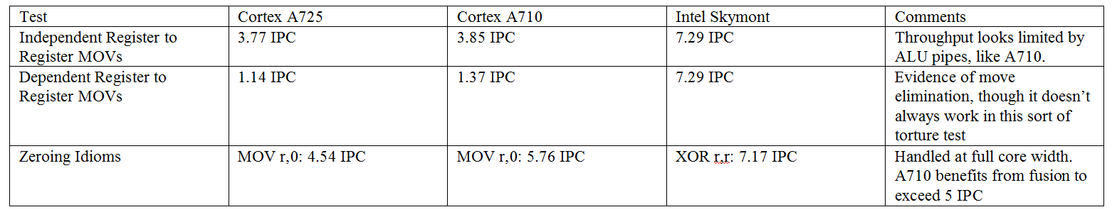
Memory renaming is another form of move elimination, where the CPU carries out zero-cycle store forwarding if both the load and store use the same address register. Intel first did this on Ice Lake, and AMD first did so on Zen 2. Skymont has memory renaming too. I tested for but didn’t observe memory renaming on A725.
Out-of-Order Execution Engine
Arm historically took a conservative approach to growing reordering capacity on their 7-series cores. A larger reordering window helps the core run further ahead of a stalled instruction to extract instruction level parallelism. Increasing the reordering window can improve performance, but runs into diminishing returns. A725 gets a significant jump in reorder buffer capacity, from 160 to 224 entries. Reordering capacity is limited by whichever structure fills first, so sizing up other structures is necessary to make the most of the ROB size increase.
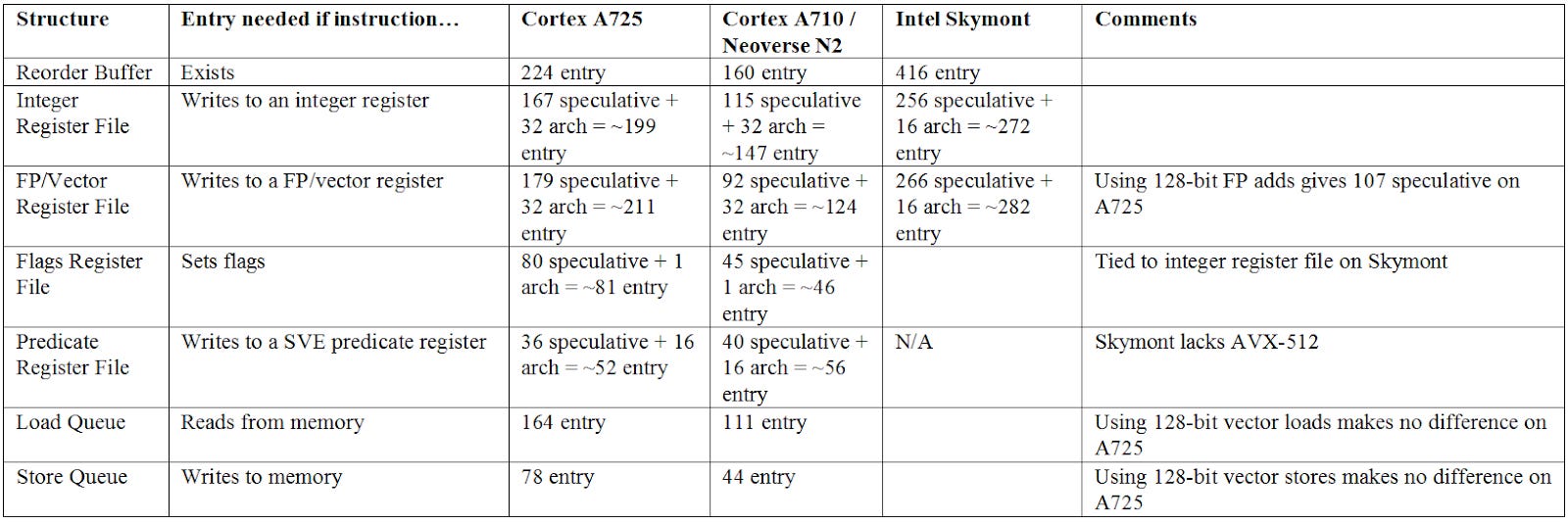
A725 gets a larger integer register file and deeper memory ordering queues, but not all structures get the same treatment. The FP/vector register file has more entries, but has fewer renames available for 128-bit vector results. FP/vector register file entries are likely 64-bit now, compared to 128-bit from before. SVE predicate registers take a slight decrease too. Vector execution tends to be area hungry and only benefits a subset of applications, so Arm seems to be de-prioritizing vector execution to favor density.
Instruction Scheduling and Execution
A725’s execution pipe layout looks a lot like A710’s. Four pipes service integer operations, and are each fed by a 20 entry scheduling queue. Two separate ports handle branches. I didn’t measure an increase in scheduling capacity when mixing branches and integer adds, so the branch ports likely share scheduling queues with the ALU ports. On A710, one of the pipes could only handle multi-cycle operations like madd. That changes with A725, and all four pipes can handle simple, single cycle operations. Integer multiplication remains a strong point in Arm’s 7-series architecture. A725 can complete two integer multiplies per cycle, and achieves two cycle latency for integer multiplies.
Two pipes handle floating point and vector operations. Arm has used a pair of mostly symmetrical FP/vector pipes dating back to the Cortex A57. A725 is a very different core, but a dual pipe FPU still looks like a decent balance for a density optimized core. Each FP/vector pipe is fed by a 16 entry scheduling queue, and both share a non-scheduling queue with approximately 23 entries. A single pipe can use up to 18 entries in the non-scheduling queue after its scheduler fills.
Compared to A710, A725 shrinks the FP scheduling queues and compensates with a larger non-scheduling queue. A non-scheduling queue is simpler than a scheduling one because it doesn’t have to check whether operations are ready to execute. It’s simply an in-order queue that sends MOPs to the scheduler when entries free up. A725 can’t examine as many FP/vector MOPs for execution ready-ness as A710 can, but retains similar ability to look past FP/vector operations in the instruction stream to find other independent operations. Re-balancing entries between the schedulers and non-scheduling queue is likely a power and area optimization.
Load/Store
A725 has a triple AGU pipe setup for memory address calculation, and seems to feed each pipe with a 16 entry scheduling queue. All three AGUs can handle loads, and two of them can handle stores. Indexed addressing carries no latency penalty.
Addresses from the AGU pipes head to the load/store unit, which ensures proper ordering for memory operations and carries out address translation to support virtual memory. Like prior Arm cores, A725 has a fast path for forwarding either half of a 64-bit store to a subsequent 32-bit load. This fast forwarding has 5 cycle latency per dependent store+load pair. Any other alignment gives 11 cycle latency, likely with the CPU blocking the load until the store can retire.
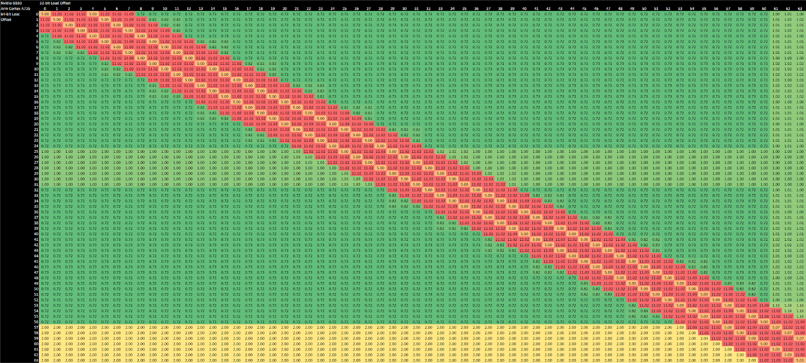
A725 is more sensitive to store alignment than A710, and seems to handle stores in 32 byte blocks. Store throughput decreases when crossing a 32B boundary, and takes another hit if the store crosses a 64B boundary as well. A710 takes the same penalty as A725 does at a 64B boundary, and no penalty at a 32B boundary.
Address Translation
Arm grew the L1 DTLB from 32 entries in A710 to 48 entries in A725, and keeps it fully associative. DTLB coverage thus increases from 128 to 192 KB. Curiously, Arm did the reverse on the instruction side and shrank A710’s 48 entry instruction TLB to 32 entries on A725. Applications typically have larger data footprints than code footprints, so shuffling TLB entries to the data side could help performance. Intel’s Skymont takes the opposite approach, with a 48 entry DTLB and a 128 entry ITLB.
A725’s L2 TLB has 1536 entries and is 6-way set associative, or can have 1024 entries and be 4-way set associative in a reduced area configuration. The standard option is an upgrade over the 1024 entry 4-way structure in A710, while the area reduced one is no worse. Hitting the L2 TLB adds 5 cycles of latency over a L1 DTLB hit.
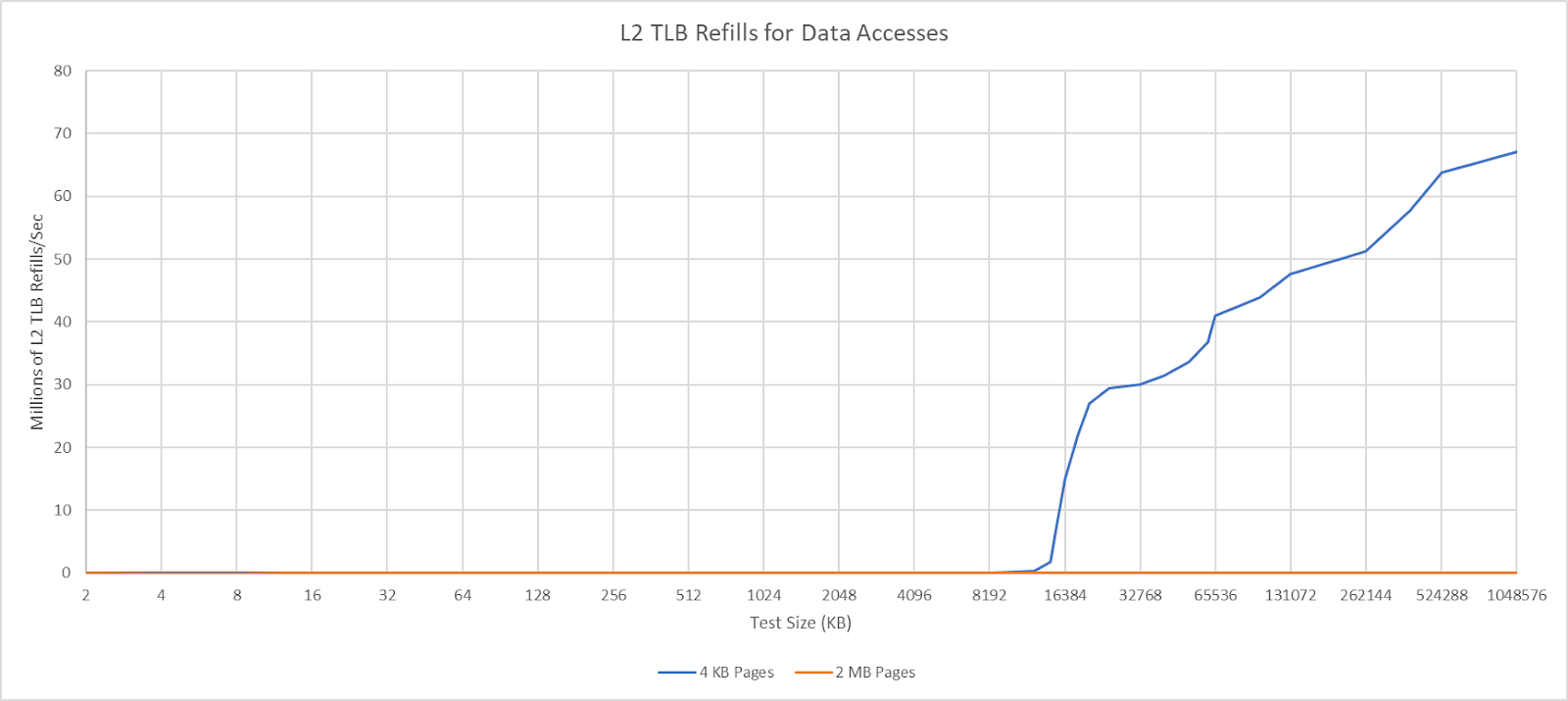
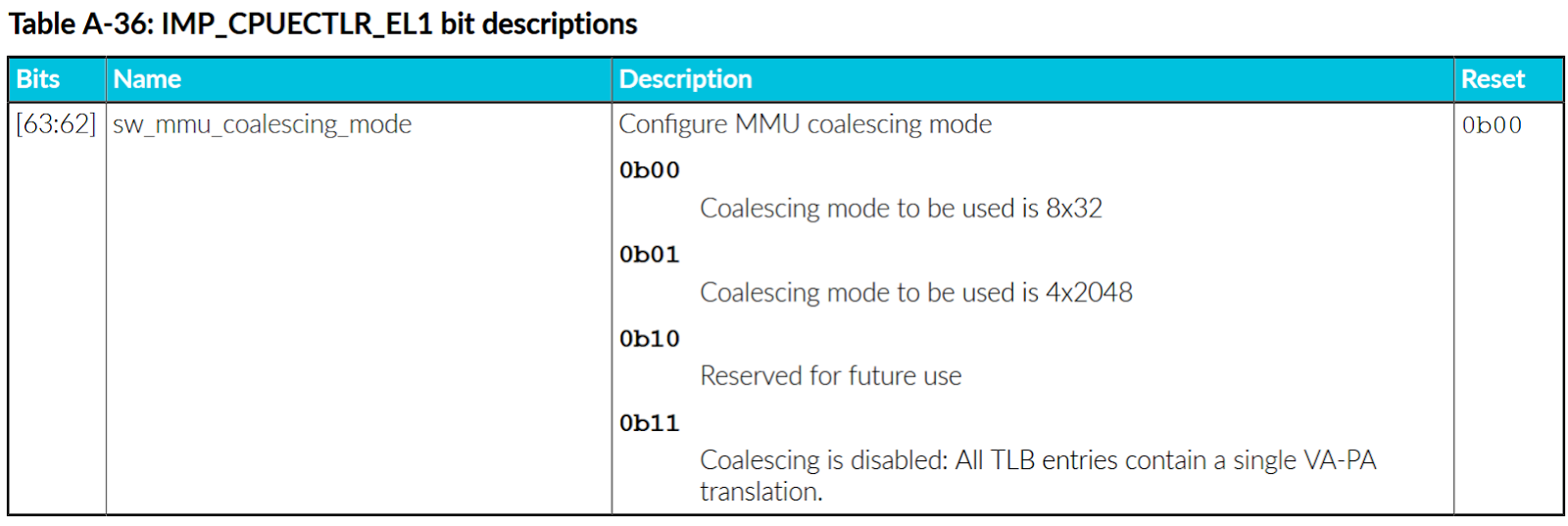
Intel’s Skymont has a much larger 4096 entry L2 TLB, but A725 can make up some of the difference by tracking multiple 4 KB pages with a single TLB entry. Arm’s Technical Reference Manual describes a “MMU coalescing” setting that can be toggled via a control register. The register lists “8x32” and “4x2048” modes, but Arm doesn’t go into further detail about what they mean. Arm is most likely doing something similar to AMD’s “page smashing”. Cores in AMD’s Zen line can “smash” together pages that are consecutive in virtual and physical address spaces and have the same attributes. “Smashed” pages act like larger pages and opportunistically extend TLB coverage, while letting the CPU retain the flexibility and compatibility benefits of a smaller page size. “8x32” likely means A725 can combine eight consecutive 4 KB pages to let a TLB entry cover 32 KB. For comparison, AMD’s Zen 5 can combine four consecutive 4 KB pages to cover 16 KB.
Core-Private Caching
A725 has a 64 KB 4-way set associative data cache. It’s divided into 16 banks to service multiple accesses, and achieves 4 cycle load-to-use latency. The L1D uses a pseudo-LRU replacement scheme, and like the L1D on many other CPUs, is virtually indexed and physically tagged (VIPT). Bandwidth-wise, the L1D can service three loads per cycle, all of which can be 128-bit vector loads. Stores go through at two per cycle. Curiously, Arm’s Technical Reference Manual says the L1D has four 64-bit write paths. However, sustaining four store instructions per cycle would be impossible with only two store AGUs.
The L2 cache is 8-way set associative, and has two banks. Nvidia selected the 512 KB option, which is the largest size that supports 9 cycle latency. Going to 1 MB would bump latency to 10 cycles, which is still quite good. Because L2 misses incur high latency costs, Arm uses a more sophisticated “dynamic biased” cache replacement policy. L2 bandwidth can reach 32 bytes per cycle, but curiously not with read accesses. With either a read-modify-write or write-only access pattern, A725 can sustain 32 bytes per cycle out to L3 sizes.
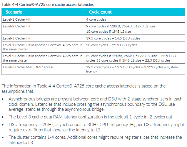
Arm’s optimization guide details A725’s cache performance characteristics. Latencies beyond L2 rely on assumptions that don’t match GB10’s design, but the figures do emphasize the expensive nature of core to core transfers. Reaching out to another core incurs a significant penalty at the DSU compared to getting data from L3, and takes several times longer than hitting in core-private caches. Another interesting detail is that hitting in a peer core’s L2 gives better latency than hitting in its L1. A725’s L2 is strictly inclusive of L1D contents, which means L2 tags could be used as a snoop filter for the L1D. Arm’s figures suggest the core first checks L2 when it receives a snoop, and only probes L1D after a L2 hit.
Performance: SPEC CPU2017
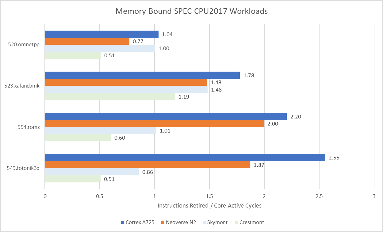
A725’s SPEC CPU2017 performance brackets Intel’s Crestmont as tested in their Meteor Lake mobile design. Neoverse N2 scores slightly higher. Core performance is heavily dependent on how it’s implemented, and low clock speeds in GB10’s implementation mean its A725 cores struggle to climb past older density optimized designs.
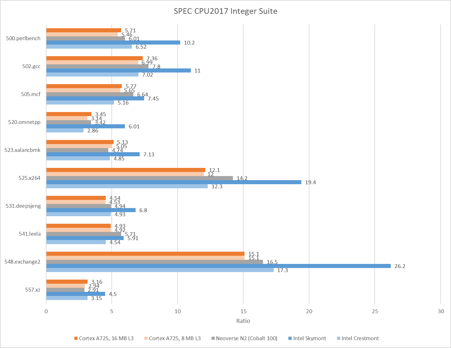
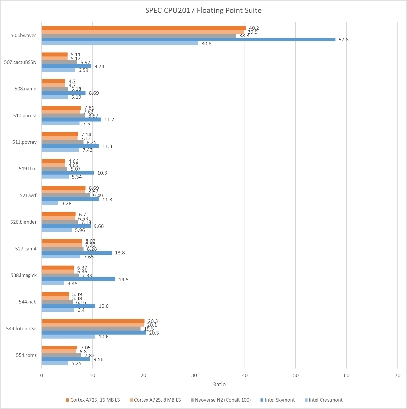
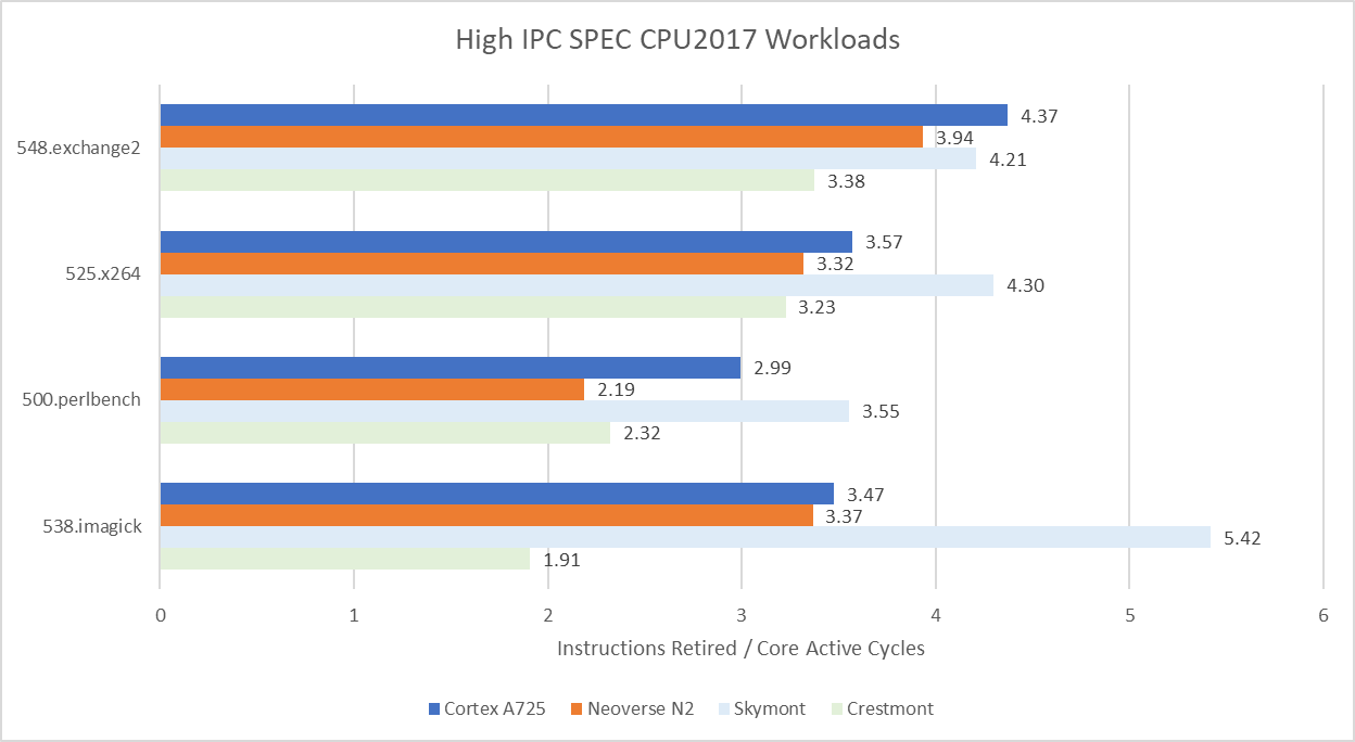
Clock speed tends to heavily influence core-bound bound workloads. 548.exchange2 is one example. Excellent core-private cache hitrates mean IPC (instructions per cycle) doesn’t change with clock speed. A725 manages a 10.9% IPC increase over Neoverse N2, showing that Arm has improved their core architecture. However, Neoverse N2’s 3.4 GHz clock speed translates to a 17% performance advantage over A725. Crestmont presents a more difficult comparison because of different executed instruction counts. 548.exchange2 executed 1.93 trillion instructions on the x86-64 cores, but required 2.12 trillion on aarch64 cores. A725 still achieves higher clock normalized performance, but Cresmont’s 3.8 GHz clock speed puts it 14.5% ahead. Other high IPC, core bound workloads show a similar trend. Crestmont chokes on something in 538.imagick though.
On the other hand, clock speed means little in workloads that suffer a lot of last level cache misses. DRAM doesn’t keep pace with clock speed increases, meaning that IPC gets lower as clock speed gets higher. A725 remains very competitive in those workloads despite its lower clock speed. In 520.omnetpp, it matches the Neoverse N2 and takes a 20% lead over Crestmont. A725 even gets close to Skymont’s performance in 549.fotonik3d.
Final Words
A725 only gains entries in the most important out-of-order structures compared to A710. Elsewhere, Arm preferred to rebalance resources, or even cut back on them. It’s impressive to see Arm trim the fat on a core that didn’t have a lot of fat to begin with, and it’s hard to argue with the results. A725’s architecture looks like an overall upgrade over A710 and Neoverse N2. I suspect A725 would come out top if both ran at the same clock speeds and were supported by identical memory subsystems. In GB10 though, A725’s cores don’t clock high enough to beat older designs.
Arm’s core design and Nvidia’s implementation choices contrast with AMD and Intel’s density optimized strategies. Intel’s Skymont is almost a P-Core, and only makes concessions in the most power and area hungry features like vector execution. AMD takes their high performance architecture and targets lower clock speeds, taking whatever density gains they can get in the process. Now that Arm’s cores are moving into higher performance devices like Nvidia’s GB10, it’ll be interesting to see how their density-optimized strategy plays out against Intel and AMD’s.
Again, a massive thank you to Dell for sending over the two Pro Max with GB10s for testing.
If you like the content then consider heading over to the Patreon or PayPal if you want to toss a few bucks to Chips and Cheese, also consider joining the Discord.
I sure hope we get a look at the x925 cores in there as well. It would be very interesting to see the structure sizes and queue depths on ARM’s most aggressive off the shelf IP.
Thanks Chester, great test and review of ARM's A725!
My (admittedly jaded) take on the slim-down of some features (vs the A710) is that, in addition to reducing area, this also reminds licensees to kindly use and pay for an X core design if they want a more performant core.
And I have this question about SVE: how much of the " de-prioritizing [of] vector execution to favor density" you observed is also because SVE sees little if any use by current software? I heard and read that many developers find SVE hard to implement, and AFAIK Qualcomm has omitted SVE entirely from their own core designs.
So, does SVE really see little use in software, is it as unwieldy as many say, and might this be the reason why ARM has now reduced its presence in their recent core designs? Thanks!