

Arm’s 5-series cores are meant for tasks where performance barely matters, but power and area efficiency are top priorities. Because they’re less performance sensitive, 5-series cores tend to be superseded less often than their more sophisticated counterparts. Cortex A53 started out Arm’s 5-series lineup in 2012, and served across three generations of 7-series cores (A57, A72, and A73). Five years later, Arm refreshed the 5-series line with the Cortex A55. A55 then served as a little core partner to A75, A76, and A78.
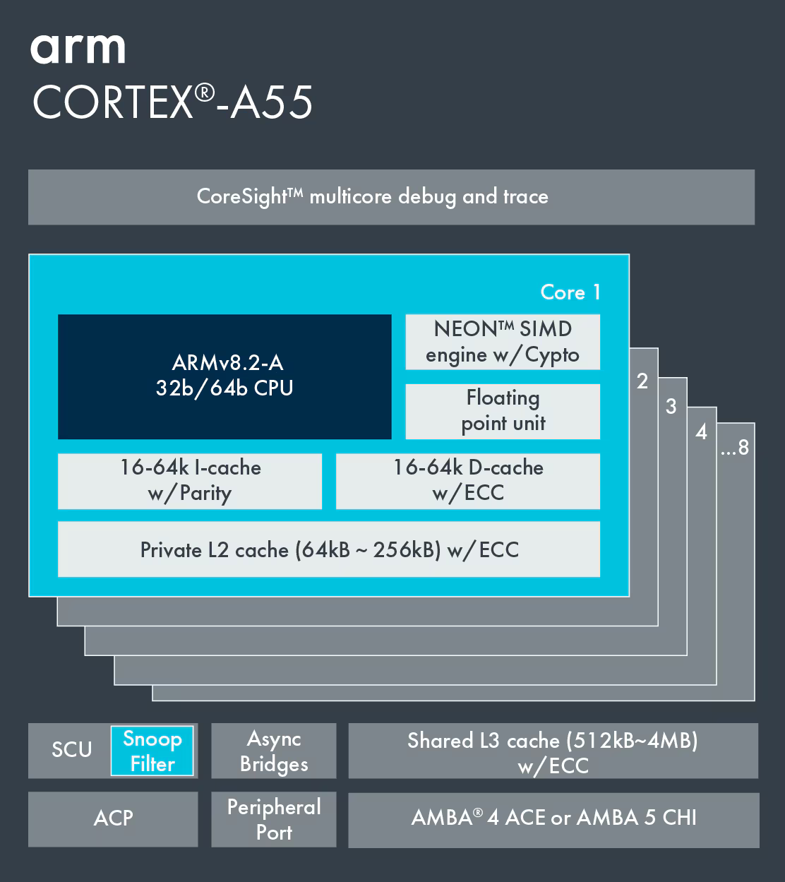
Here, I’ll be looking at the A55 primarily in the Mediatek Genio 1200, using the Radxa NIO 12L single board computer. The Mediatek Genio 1200 has four A55 cores and four A78 cores in what Arm calls the DynamIQ Shared Unit (DSU). The DSU is a cluster with 2 MB of L3 cache, and can host different core types without creating cluster boundaries between them. The Genio 1200 runs its A55 cores at 2 GHz, and gives each A55 core 128 KB of L2 cache. For memory, the SBC comes with 8 GB of LPDDR4X running at 4266 MT/s.
I’ve somehow wound up with several A55 implementations. My previous phone, a Pixel 3A, has a Snapdragon 670 with six A55 cores. Zarif98 on Reddit kindly donated a OnePlus 7 Pro, and that comes with four A55 cores in the Snapdragon 855. Microbenchmarking on Linux is easiest because Android tends to be a noisy environment, but I’ll occasionally include data from those devices to show whether an observation comes down to implementation differences.
Overview
Arm’s Cortex A55 retains A53’s 2-wide, in-order execution formula and makes targeted improvements. Like its predecessor, A55 uses an eight stage integer pipeline and a nine stage floating point one. All instructions pass through every pipeline stage for their category, which ensures ordering and avoids writeback conflicts from different latency instructions finishing at the same time. That makes the pipeline more fixed length than in a typical out-of-order core.
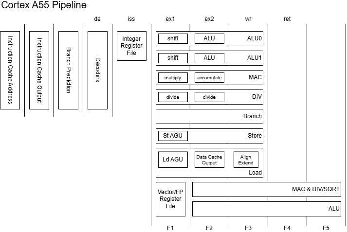
A55’s improvements are concentrated in the frontend and memory subsystem, though parts of the core proper received tweaks as well.
Branch Prediction
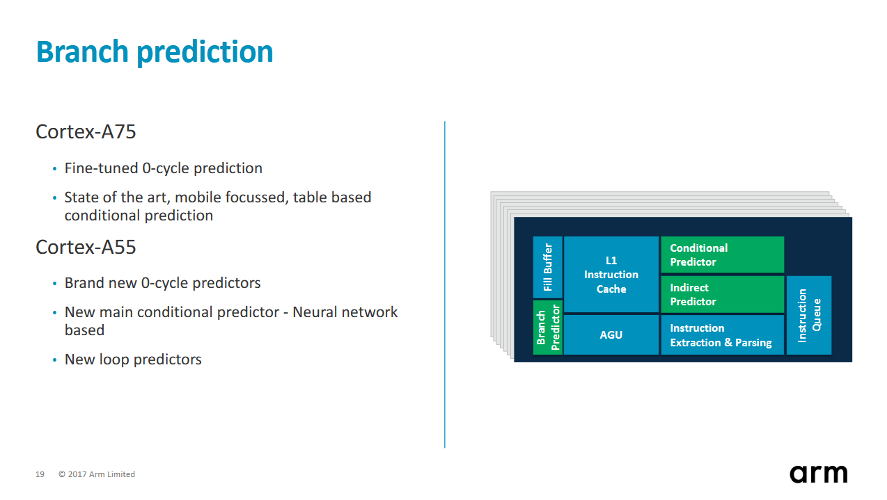
Arm’s slides talk about a new “neural network based” predictor. This likely means A55 uses a perceptron predictor, which can learn longer patterns while requiring less growth in predictor storage than the A53’s GShare predictor.
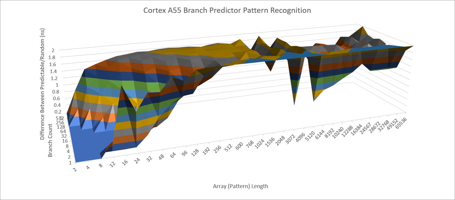
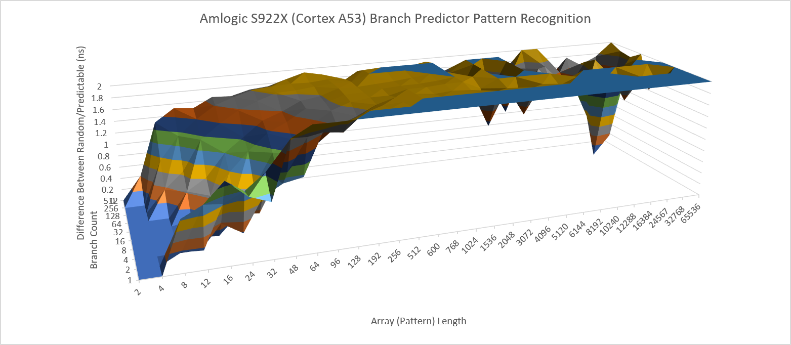
Testing with branches that are randomly taken/not-taken in random patterns of increasing lengths shows A55 doing better than its predecessor. However, it’s still far off contemporary high performance cores.
A55 and A53’s performance counters make a like-for-like comparison difficult because A53’s performance monitoring unit (PMU) can’t restrict counting to retired branches. A rough comparison with retired branches on A55 and executed branches on A53 suggests some level of improvement across Geekbench 6’s workloads, though it’s hard to tell how significant that difference is.
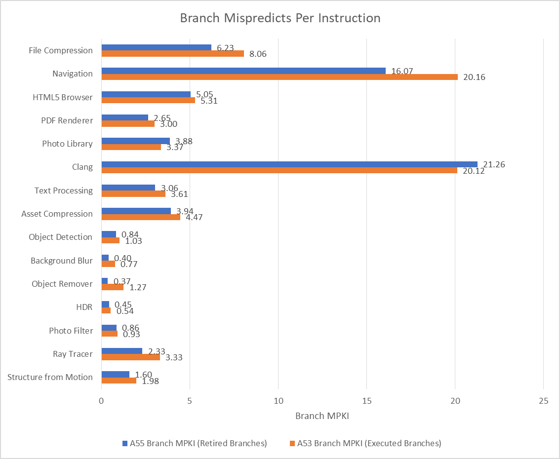
Curiously, A55 doesn’t universally improve and suffers more mispredictions in Clang. Photo Library is another case where A55’s newer predictor doesn’t show a clear benefit. Tuning predictors is difficult especially with bare bones power and area budgets, so some applications are bound to fall through the cracks. Perceptron predictors also struggle to predict linearly inseparable patterns. Schemes that index into a history table using the global history don’t have that problem.
Branch prediction speed can affect frontend throughput, and A55 improves that with a new 48 entry micro-BTB. This micro-BTB can handle taken branches without introducing pipeline bubbles, and should speed up performance in tight loops with taken branches. A53 had a 16 byte branch target instruction cache (BTIC) that could accelerate instruction delivery, but only for a single branch target. A 48 entry micro-BTB is still small, but should be relevant for more cases. Branch spacing doesn’t affect micro-BTB capacity.
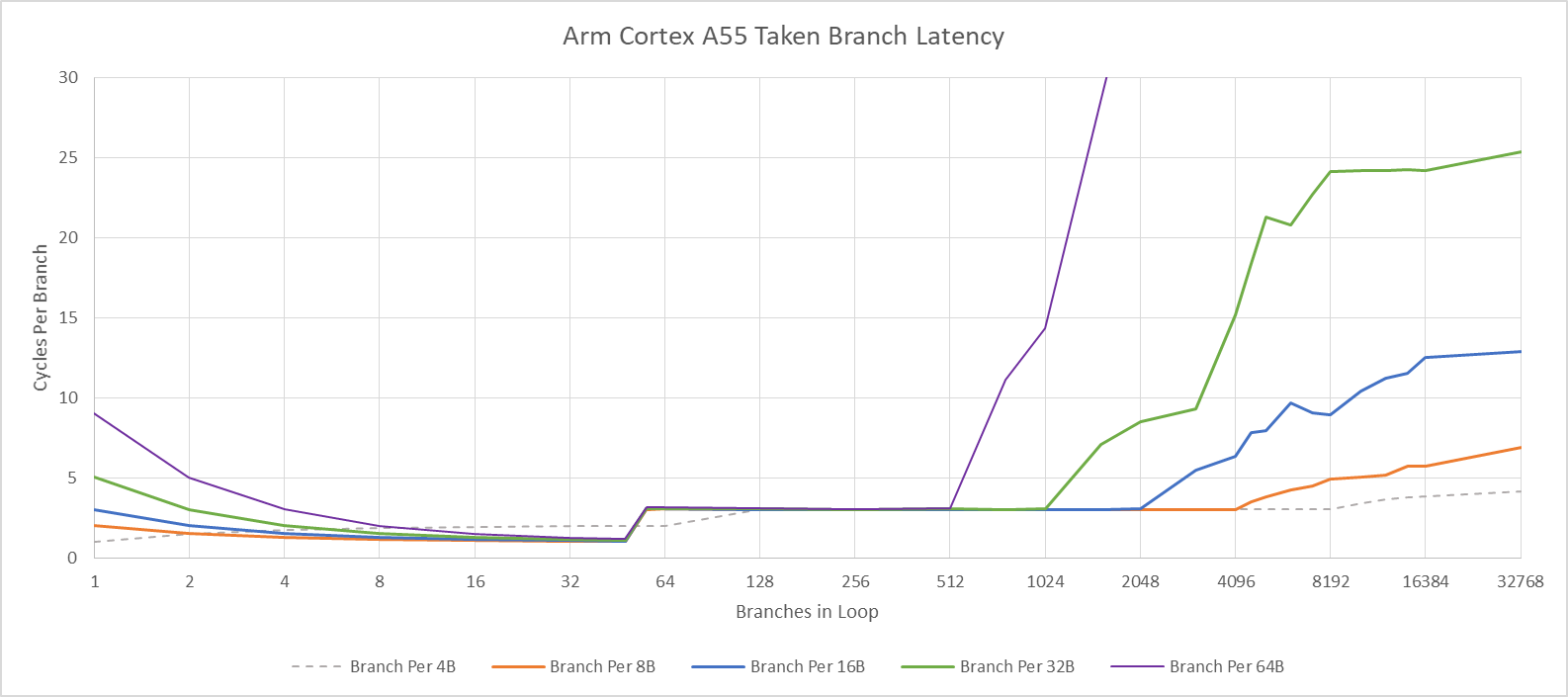
A55 continues to lack a large BTB with hundreds or thousands of entries like on high performance cores. The core’s decoders calculate target addresses for taken branches not captured by the micro-BTB, giving taken branches 3 cycle latency like on A53. It’s not bad for code that fits in the instruction cache, especially considering that in-order cores are likely to lose lots of throughput from data-side memory latency. However, it does mean the branch predictor can’t run ahead of instruction fetch and drive long distance prefetch.
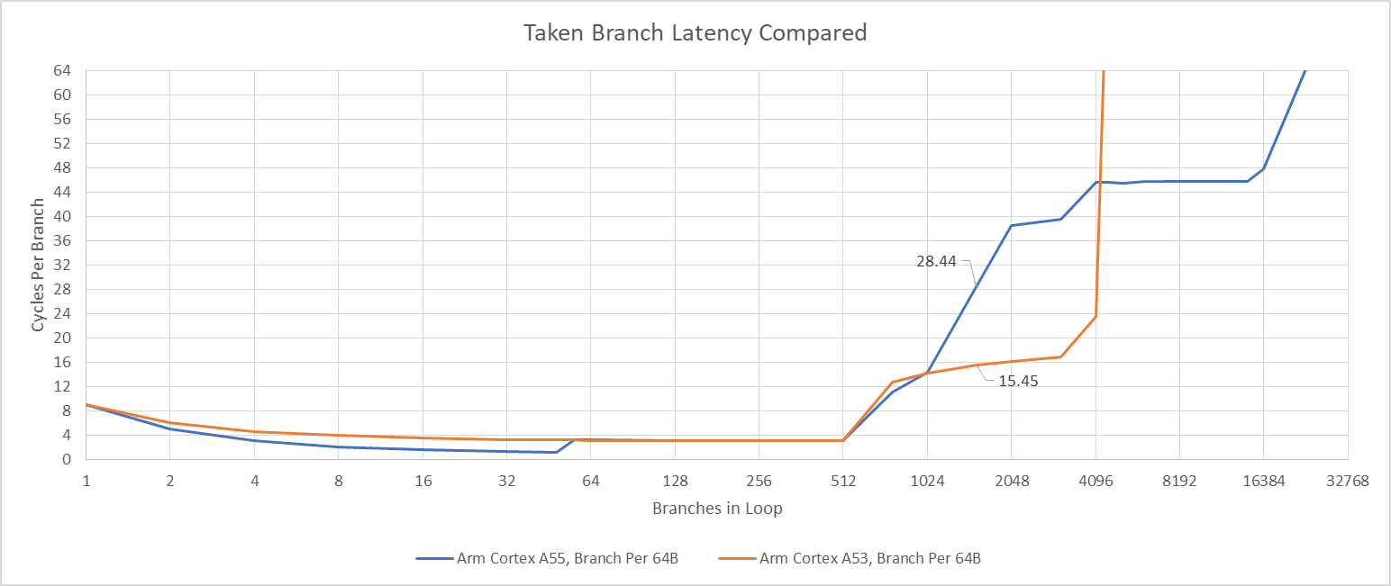
If each branch jumps to a different 64B cache line, taken branch latency heads for the skies once the test exceeds instruction cache capacity. A55 curiously regresses compared to A53, even though A55’s private L2 cache offers better data-side latency than A53’s larger shared one. With 1536 branches (96 KB), A55 averages 28-29 cycles per taken branch compared to 15-16 cycles on A53.
Instruction Fetch
Cortex A55 comes with 16 KB, 32 KB, and 64 KB options. Compared to A53, Arm dropped the 8 KB option and increased associativity from 2-way to 4-way. Increased associativity reduces the likelihood of conflict misses, where the cache may have enough capacity to contain frequently accessed lines, but ends up getting thrashed because of restrictions on where those lines can be stored.
A55’s instruction cache stores instructions in a pre-decoded format to reduce decode costs, rather than storing raw instruction bytes. 4 byte aarch32 or aarch64 instructions are expanded to a 40-bit intermediate format, while 16-bit T32 (Thumb) instructions take 20 bits. Instruction cache tags indicate the instruction type (aarch32, aarch64, or T32). The predecode approach is common to many of Arm’s cores, and takes a midpoint between a conventional instruction cache and a micro-op cache that completely skips decoding.
Instruction cache tags and data are parity protected, with one parity bit per 32-bit tag entry and one bit per 20 raw data bits. That means A55 can detect a single bit error within each predecoded T32 instruction, or up to two flipped bits in a 4B instruction provided the two bits don’t occur in the same 20-bit half.
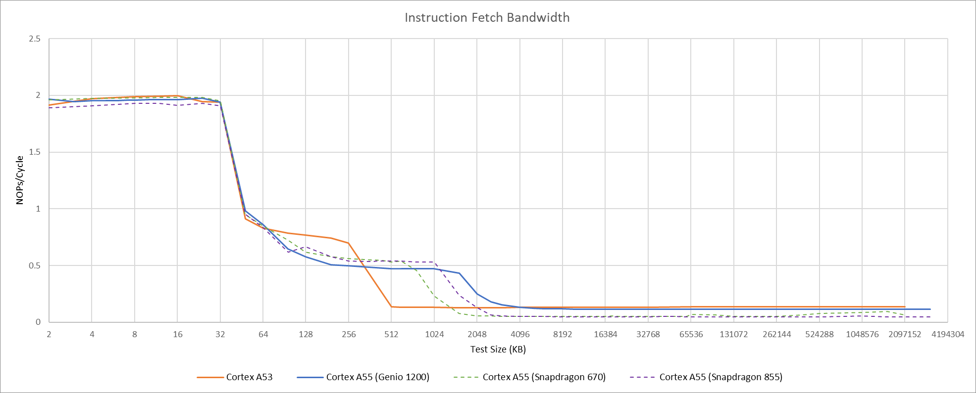
Mediatek and Qualcomm chose the 32 KB option for their chips. Testing with a loop of NOPs gives no surprises. All A55 implementations can sustain two instructions per cycle from the instruction cache. Spilling out of L1I drops throughput to well below 1 IPC. Arm’s Technical Reference Manual states that the instruction cache has a “128-bit read interface to the L2 memory system”. However, A55 can’t seem to fully utilize that interface in a sustained fashion in this simple test. A55 also displays lower code throughput than A53 out of L2, mirroring the situation with branches. Past L2, A55 regains the lead because it benefits from a L3 cache.
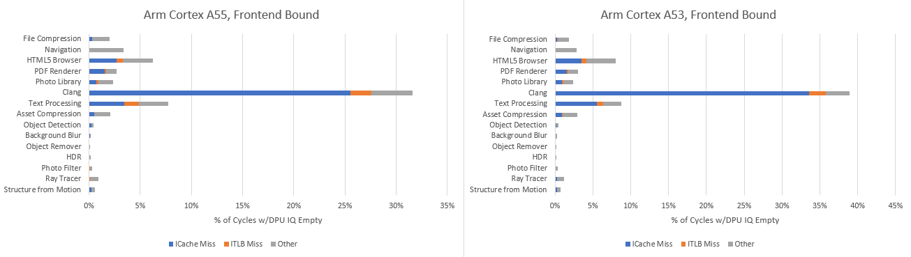
Geekbench 6 shows A55 and A53’s frontends facing similar challenges. A55/A53 are both organized into an Instruction Fetch Unit (IFU) and Data Processing Unit (DPU). The DPU decodes and executes instructions, and contains an instruction queue. Arm treats cycles with an empty DPU instruction queue as frontend bound. I’m applying the same definition to A53, even though Arm didn’t use top-down metric definitions in A53’s time. Workloads with larger instruction footprints, like Clang, cause the DPU IQ to stay empty for a significant fraction of core cycles. Further breaking down the cause shows most of this happens when there’s an instruction cache miss pending. A55’s higher L1I associativity may help a little bit, but not having a large decoupled BTB continues to hurt.
Backend (DPU)
A55 inherits most of A53’s backend, meaning it features robust dual-issue capability. Most instructions can issue from either position, and the core has two copies of execution units for the vast majority of common instructions. Interlocks take care of instruction dependencies, meaning that adjacent dependent instructions don’t cause issue-stage hiccups. Forwarding paths help deliver low execution latency even though the pipeline is fixed length.
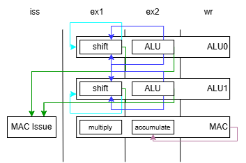
Earlier, I applied the same methodology I used to measure structure sizes on out-of-order CPUs to A53. Those tests showed A53, and A55, could do limited reordering around a cache miss. I assumed that was because the DPU had some kind of buffer for tracking in-flight operations in the backend. After reading the optimization guides for both cores, I think a better explanation is that independent instructions issued after a load can sit in pipeline stages while waiting for the load to retire. If so, observed reordering distance is simply the number of pipeline stages that younger instructions can occupy (or the first pipeline hazard that forces an issue-stage stall). There’s no pseudo-ROB.
A55’s execution pipe layout is basically unchanged. However, floating point fused multiply-add (FMA) instructions see latency reduced to 4 cycles, down from eight in A53. FP adds and multiplies have 4 cycle latency, so A53’s 8 cycle FMA latency meant there was no latency advantage to using FMA. A55 fixes that situation. Elsewhere, A55 receives changes to support the Armv8.2 standard, as well as LDAPR from Armv8.3 and dot product instructions from Armv8.4. Arm’s reluctance to pursue larger execution-side changes is understandable. Performance often comes down to feeding execution units rather than having more of them, and in-order cores face severe challenges in keeping their execution units fed.
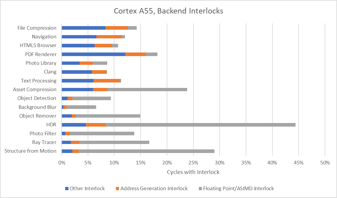
Many of Geekbench 6’s workloads are heavy on FP/SIMD instructions. A55 cuts down floating-point/vector related interlocks in Asset Compression, HDR, Photo Filter, and Ray Tracer.
Structure in Motion doesn’t benefit, though that could be a case of A55’s improved memory subsystem shifting bottlenecks away from load latency and towards the execution units. Integer workloads like File Compression and Navigation see little change in interlock delays between the two cores.
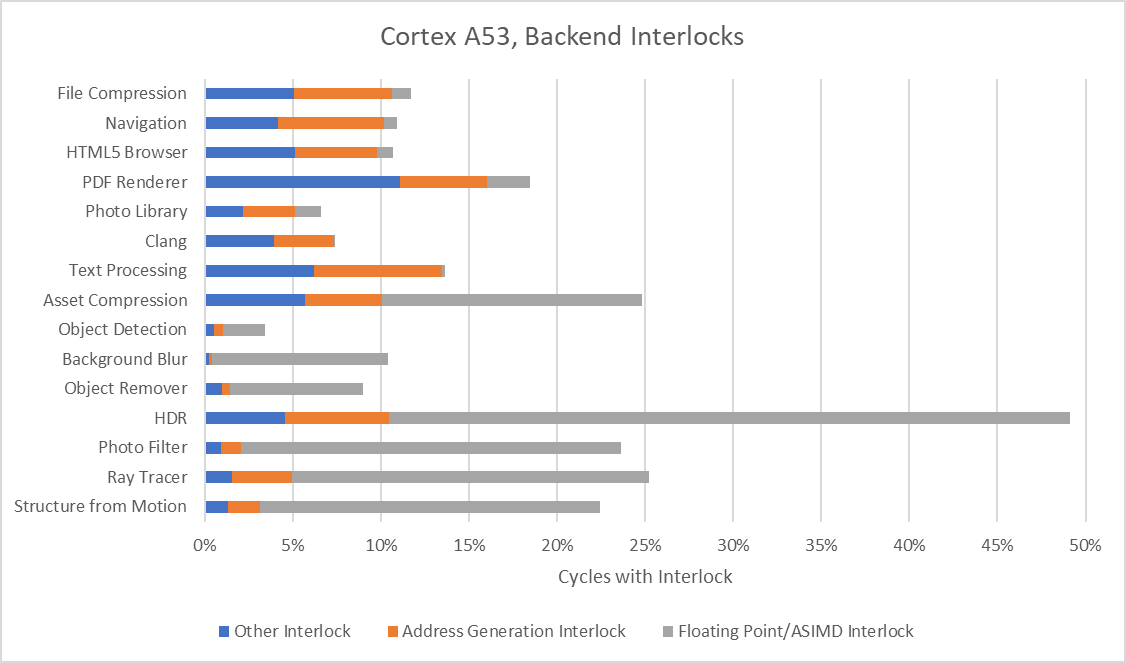
At a higher level, A55 and A53 both have weak vector execution units. Even though there are two floating-point/vector pipelines, each pipeline only has 64-bit vector execution width. FP/vector operations also have longer latency than scalar integer ones. Out-of-order cores can easily absorb 4 cycle latency, but that’s not always the case for in-order cores.
Load/Store
Arm delivered more significant improvements to the memory subsystem, which starts with the load/store unit on the data side. A55 can now sustain both a load and a store every cycle, compared to A53’s single memory operation per cycle. Load and store bandwidth individually remain unchanged at 8B/cycle for loads and 16B/cycle for stores. However, the improved dual issue capability can be particularly beneficial for memory copy routines that don’t put loads and stores too far apart.
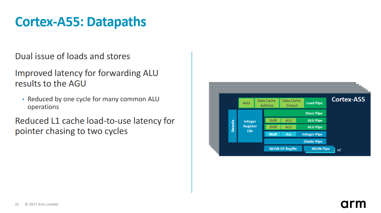
A55 improves L1D hit latency too thanks to an adjusted load pipeline and a forwarding path from the beginning of the load writeback stage to the AGU’s base operand input. This forwarding path lets A55 achieve two cycle latency for dependent loads. The load writeback stage can also forward to the ALUs, giving 2 cycle load-to-use latency for ALU operations as well.
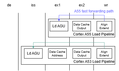
Curiously, it seems like A55 can only use one of those fast forwarding paths at once. Placing an ALU instruction between two dependent loads increases pointer chasing latency to three cycles, but only if that ALU instruction consumes the prior load’s result. An independent ALU instruction doesn’t increase latency.
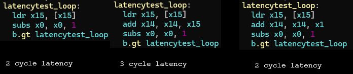
Indexed addressing increases load latency to three cycles, which is still one cycle faster than doing the same on A53. A53’s optimization guide interestingly mentions two cycle pointer latency as well, though I have not been able to achieve that even with unrolled back-to-back dependent loads. I’m not sure how A53’s pipeline layout would allow for two cycle load latency in any case. A load would need three clock transitions to get from the AGU to the writeback stage, and A53’s optimization guide says forwarding happens from the beginning of the writeback stage.
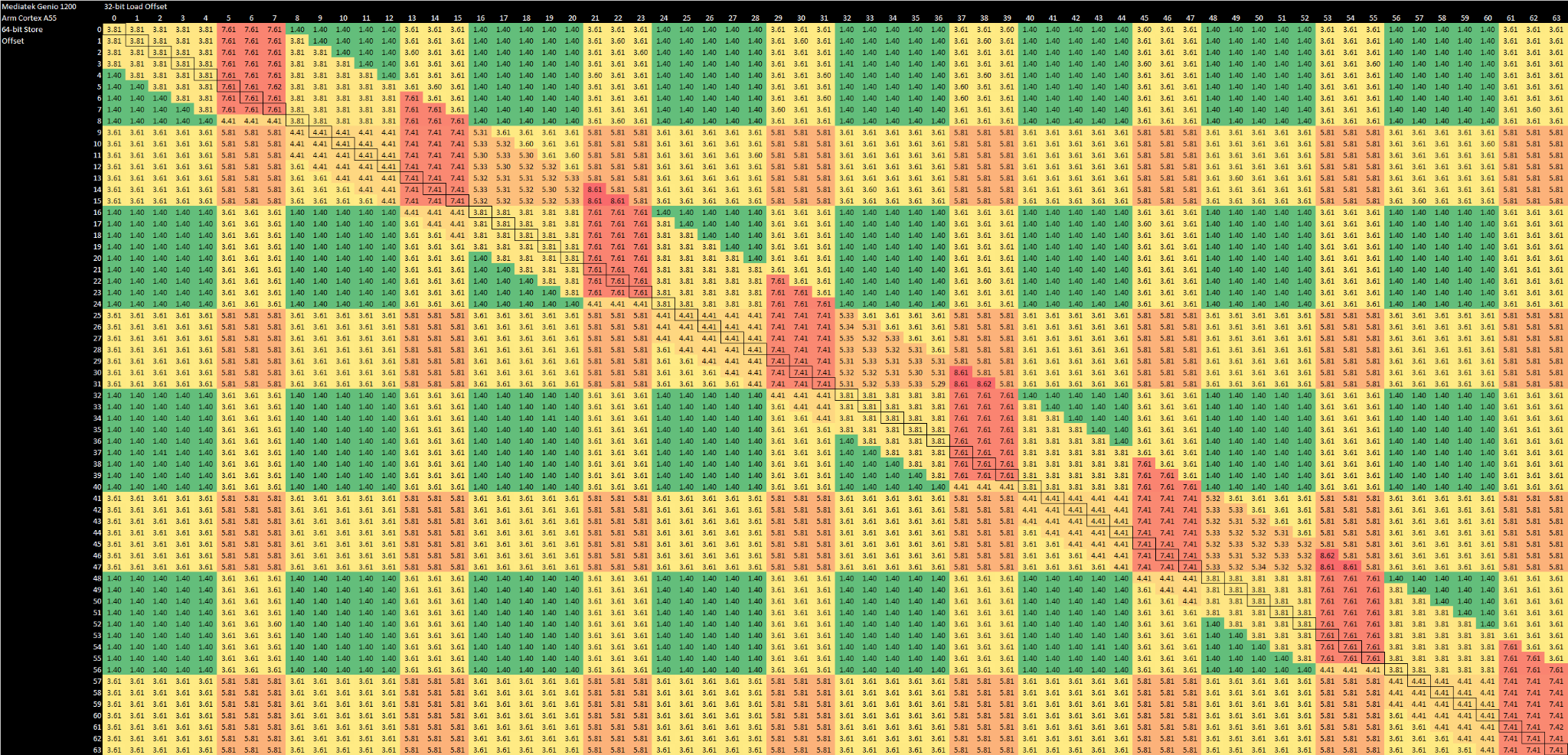
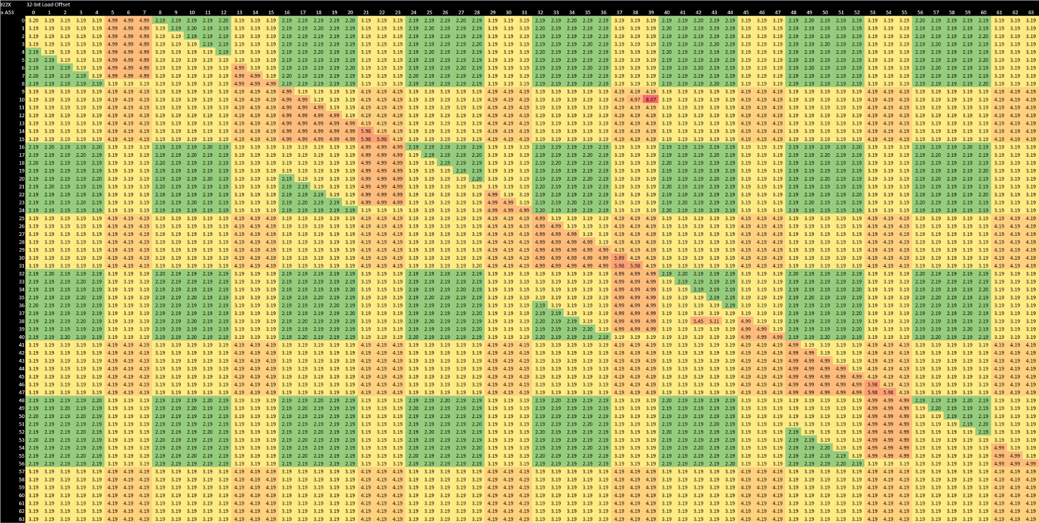
Store forwarding latency increases on A55 compared to A53, though cycle count latencies remain low compared to many out-of-order cores. Perhaps supporting dual issue made A55’s load/store unit more complex, and introduced extra penalties. To summarize the notable cases:
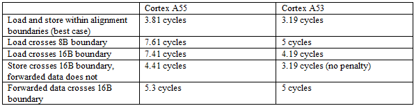
A55 continues to prefer 8B alignment for loads and 16B alignment for stores. Both cores avoid harsh penalties when a load only partially overlaps a prior store, likely thanks to their simple in-order designs and short pipeline depth. A55’s latency regression versus A53 probably has little effect because an in-order core can’t have hundreds of instructions in flight, making store forwarding cases less likely.
Cache misses are handled similarly on A53 and A55. Neither core supports hit-under miss, so any L1D miss will delay subsequent memory accesses even if they hit L1D. A55/A53 can achieve some degree of memory level parallelism by letting loads after a cache miss access L1D and generate fill requests. A55/A53 can generate up to three outstanding cache refill requests this way. Arm’s optimization guide says that only works if the three loads are within four pipeline stages of each other.
Address Translation
In typical scenarios, every memory access uses a virtual address that has to be translated on-the-fly to a physical address that corresponds to locations in DRAM or IO. A55 uses two translation lookaside buffer (TLB) levels like many other cores. TLBs cache frequently used translations, helping reduce address translation penalties. A55’s first level TLB has 16 entries, up from 10 in A53. Both figures are small compared to even older out-of-order cores. AMD’s Athlon 64 from long ago had 32 entry L1 TLBs, for reference. L2 TLB size is more reasonable at 1024 entries, matching Intel’s Haswell, and has twice the capacity of A53’s 512 entry L2 TLB.
Getting a translation out of the L2 TLB adds three cycles of latency, compared to just two on the A53. It’s a good tradeoff because the larger first level TLB should reduce reliance on the L2 TLB, and an in-order core will struggle to deal with page walk latency. 3 cycles of L2 TLB latency is good compared to many out-of-order cores, including low clocked ones. A78 for example takes 5 extra cycles of latency on a L2 TLB hit.

To reduce page walk cost, Arm uses both an Intermediate Physical Address (IPA) cache and a walk cache. The IPA cache holds translations between a VM’s physical address and host physical address, helping reduce virtualization overhead. The walk cache holds the second-to-last translation table entry, letting page walks initialize with one step to go. Arm didn’t change IPA cache or walk cache size on A55, likely because 64 entries already go a long way. One translation table holds 512 entries, so 64 walk cache entries would already accelerate page walks for up to 128 MB of address space using 4 KB pages.
L2 TLB structures are parity protected, with parity errors causing an invalidation and a page walk.
Cache Setup
A55’s L1D cache has 16 KB, 32 KB, and 64 KB options, and is 4-way set associative like the L1I cache. L1D data and tags are ECC protected, with single-bit errors handled by evicting the line, correcting the error as part of the eviction process, and reloading the line from L2. Compared to A53, increased L1D associativity should provide a slight hitrate improvement. Arm also changed L1D addressing from physically indexed, physically tagged (PIPT) in A53 to a virtually indexed, physically tagged (VIPT) scheme in A55. Note that the 32 KB and 64 KB options are still VIPT. A common misconception is that VIPT requires the virtual address bits that give the offset into a page to exactly match the cache index bits.

Cache misses are the most common long latency instruction in most workloads, and present a severe problem for in-order cores. A55 and A53 can keep no more than about eight instructions in flight after a cache miss, which is four cycles of core throughput. Any L1D miss will incur a longer penalty than four cycles, so reducing cache miss latency is crucial to making the situation less bad. A55 also needs to support Arm’s new DynamIQ Shared Unit (DSU), which has different cache setup expectations.
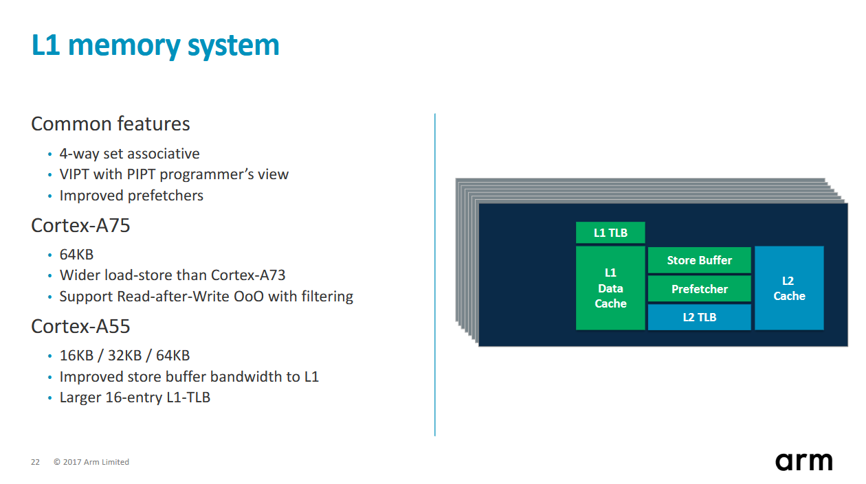
As a result, A55 gets an optional core-private L2 cache, which aligns with the DSU’s expectations and allows for lower L2 hit latency. A55’s L2 mostly acts as a victim cache, though software prefetch instructions can bring data into L2 without first getting that data evicted from L1. Arm provides 64 KB, 128 KB, and 256 KB L2 capacity options, all of which use 64B cache lines and are 4-way set associative. The L2 has a 128-bit write path and 64-bit read path to the core, matching load/store bandwidth. An extremely area constrained design can have no L2 cache, though doing so would likely be catastrophic for performance. 128 KB seems to be a popular choice, and is what Mediatek picked in the Genio 1200.
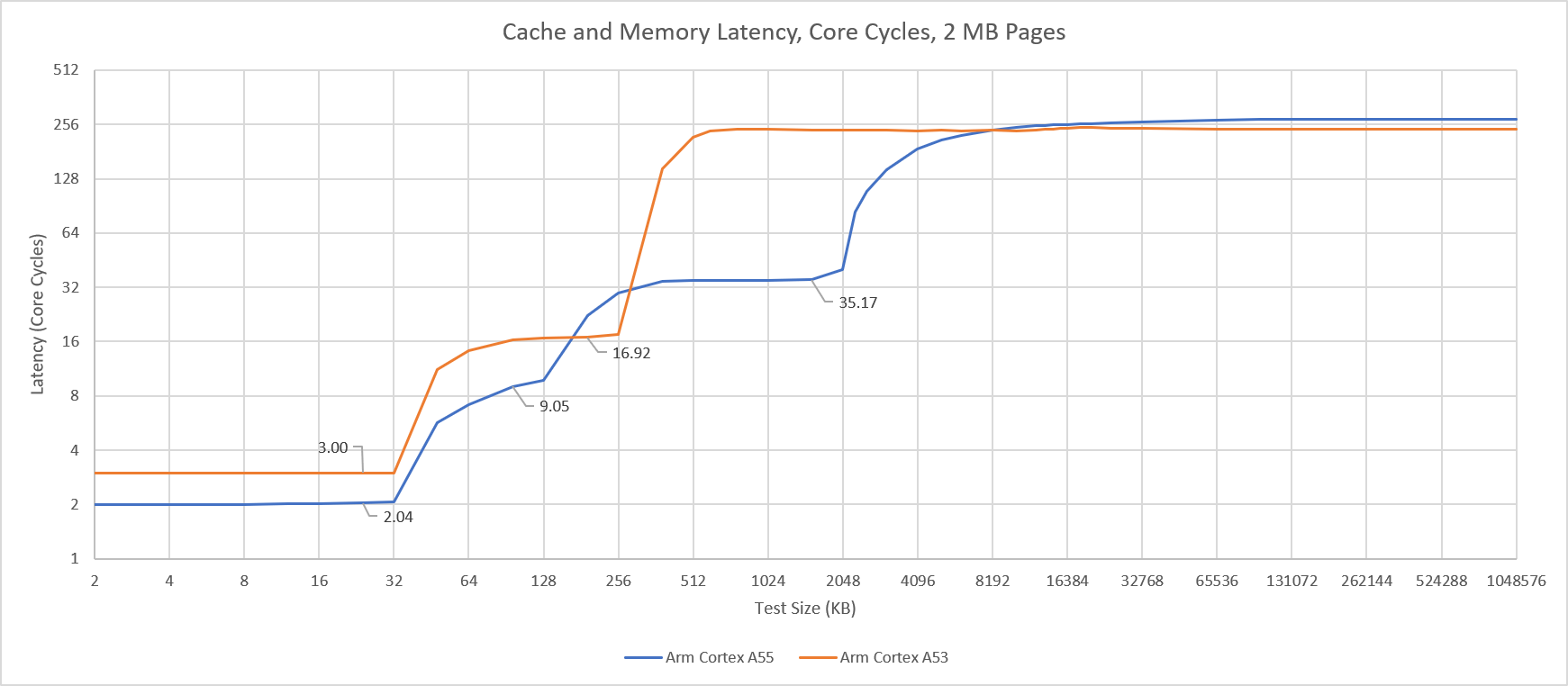
L2 latency comes in at a brisk 9 cycles, or just over half the 17 cycle latency seen with A53’s 256 KB shared L2 A small 32 KB L1D will see a lot of misses, and a 128 KB L2 could service a significant portion of those misses without the latency of a shared cache. The downside is that four 128 KB caches require twice the storage capacity of a single shared 256 KB cache.
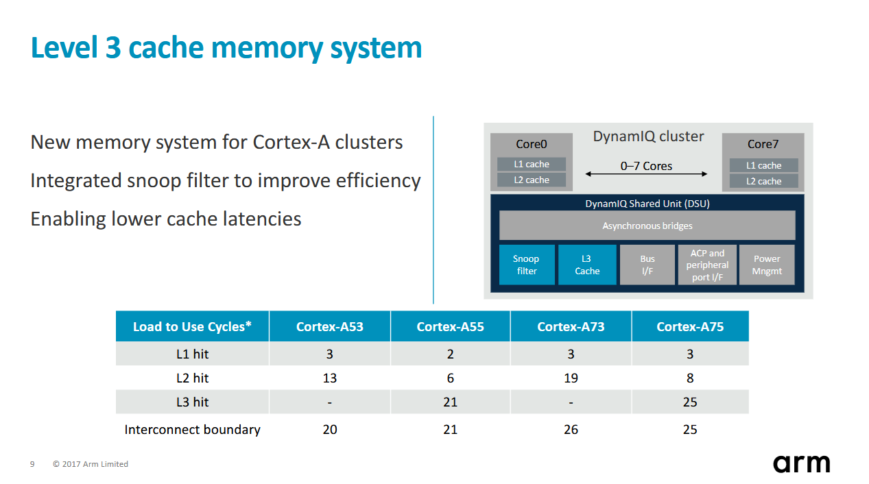
With the new core-private L2, the DSU’s L3 takes over the role of a large, last level shared cache. Arm’s first DSU, the one introduced with A55 and A75, supports up to 4 MB of L3. L3 capacity options larger than 1 MB use two slices, meaning the Genio 1200’s 2 MB L3 is built from two slices. The power of two size also means it’s 16-way set associative. Arm allows 1.5 MB and 3 MB L3 options by disabling ways to create a 12-way cache.
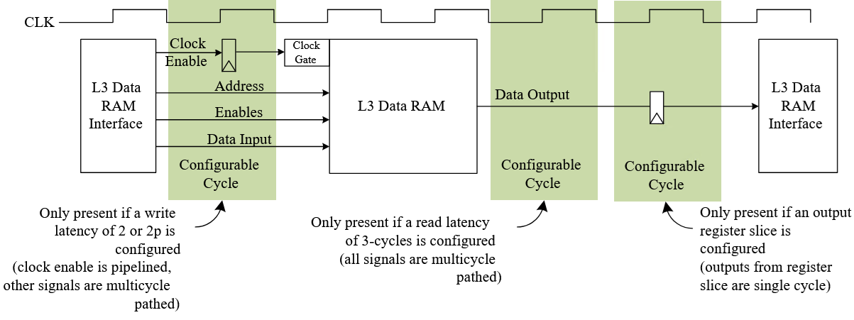
L3 latency varies depending on implementation options, with Arm giving a 21 cycle latency example. On the Genio 1200, L3 latency comes in at around 35 cycles. It’s much higher latency than the 256 KB L2 on the Amlogic S922X’s A53 cluster, but that’s understandable considering the Genio 1200 has eight cores in the cluster instead of two. On the capacity front, A53 did support L2 capacities up to 2 MB, but I doubt that was a common configuration.
Bandwidth tends to be de-prioritized for density optimized designs, and Arm’s 5-series cores sit far on the density optimized side of the spectrum. Still, A55 manages significant bandwidth improvements at larger test sizes. A53’s bandwidth crashes into the ground once test sizes spill out of cache. A55’s results vary across implementations, but all display milder bandwidth dips even after test sizes exceed L3 capacity. Mediatek’s Genio 1200 barely shows any single thread bandwidth decrease even at very large test sizes.
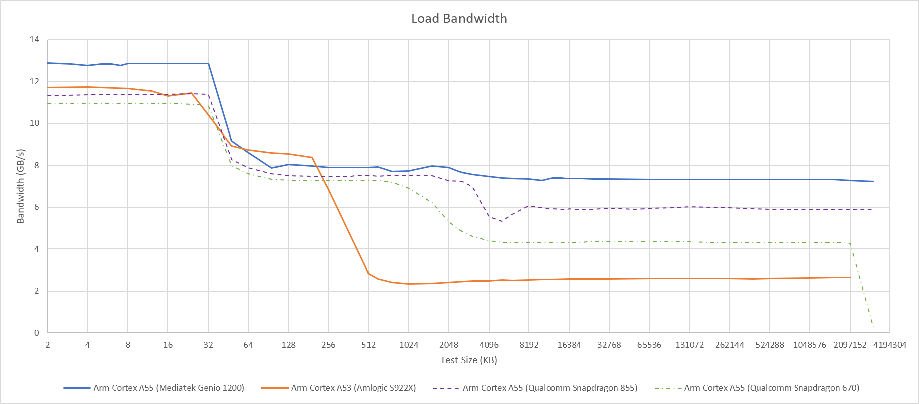
Part of this could come from prefetching. A55/A53 rely heavily on prefetch to achieve memory level parallelism, because both cores can only sustain three L1D demand misses. Arm’s documentation indicates that A55’s L1D prefetcher can make up to seven outstanding prefetch requests, with a default of five. Curiously, A53 can be configured to make up to eight outstanding prefetches. New in A55 though is a L3 prefetcher that can be configured to prefetch 32 lines ahead, with eight lines as the default. Prefetch into L3 can be more aggressive, because the L3 cache’s larger size reduces the chance of useless prefetches contending with frequently used lines. This more aggressive prefetch likely explains A55’s higher memory bandwidth.
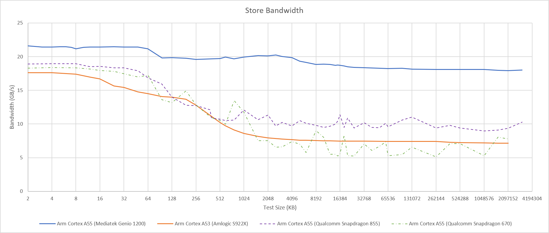
Both A55 and A53 use a streaming mode to help store bandwidth, with a switch at each cache level triggered by reaching a threshold of consecutive “streaming” cache lines. Mediatek’s A55 cores maintain very high store bandwidth even across large test sizes, mirroring behavior with loads. Other A55 implementations show similar behavior to A53.
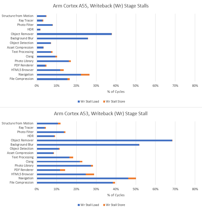
Performance counters show A55’s memory subsystem delivering impressive improvements. Memory-related stalls were severe on A53, especially on Geekbench 6’s Object Remover, Background Blur, and Navigation workloads. A55 nearly cuts those figures in half.
Performance
The A55 cores on Mediatek’s Genio 1200 deliver performance improvements well above Arm’s reference figures across many of Geekbench 6’s workloads. Background Blur enjoys an astounding 210% score uplift, thanks to being less memory bound and suffering fewer FP/SIMD interlocks. Gains are also massive in Object Detection and Photo Filter.
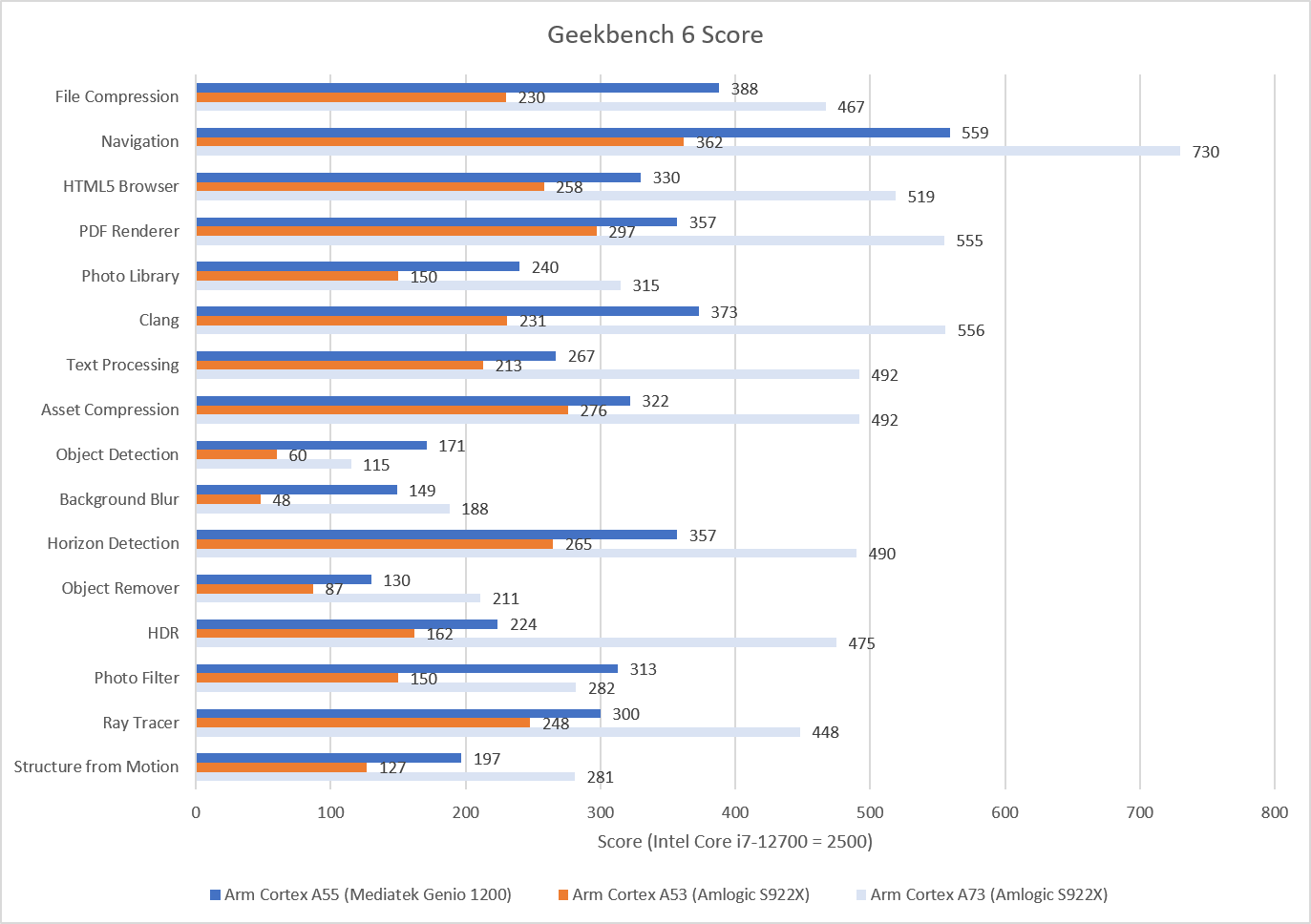
I suspect uplifts will be closer to Arm’s estimates in a more like-for-like comparison. Mediatek’s Genio 1200 does give its A55 cores a much stronger memory subsystem than the Amlogic S922X does for its A53 cores. But better caching would be expected from most A55 implementations, thanks to the new DSU setup’s expectations.
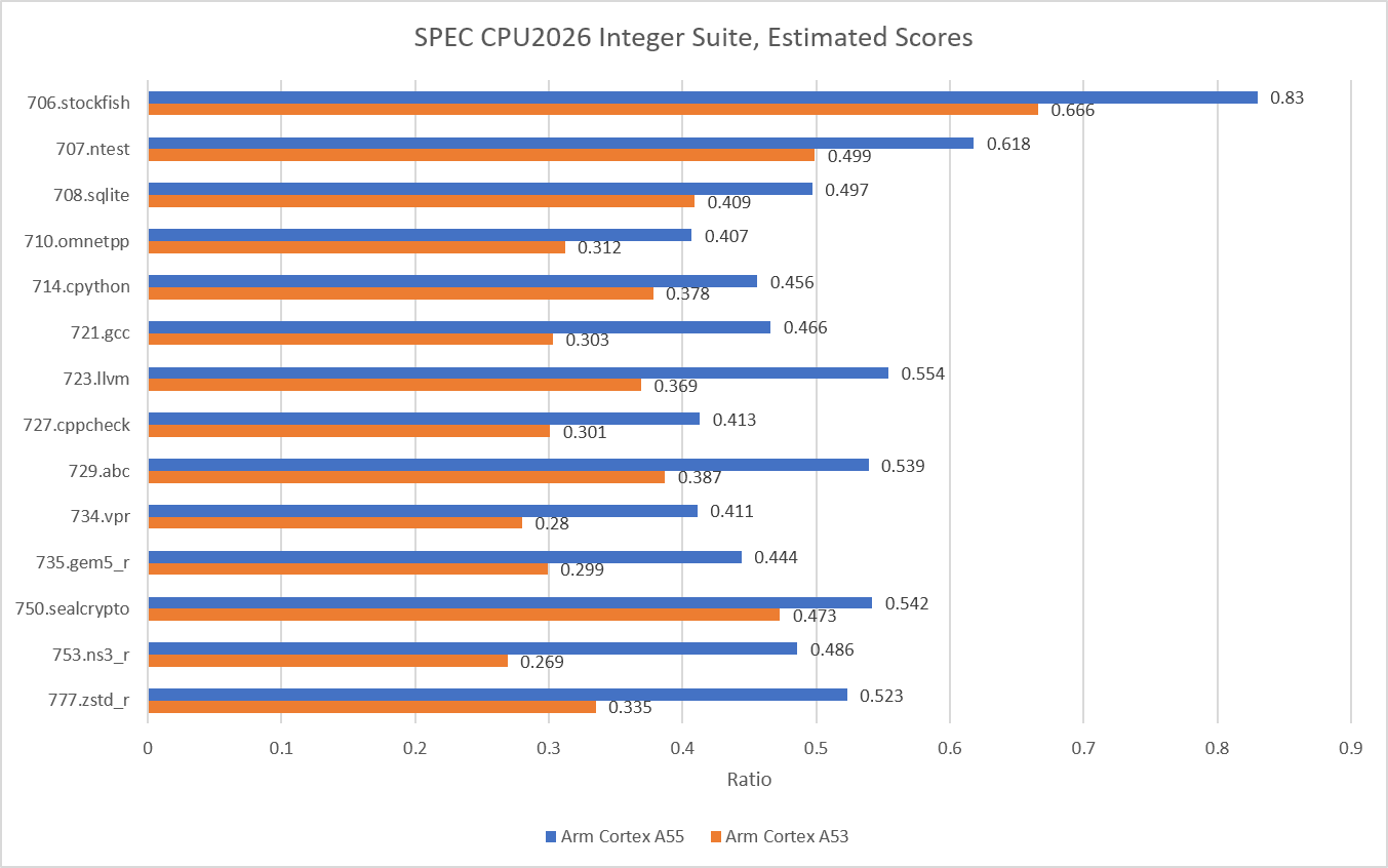
A55’s improvements are less impressive in SPEC CPU2026’s integer suite, though they still go beyond typical generation-on-generation gains from high performance cores. A 35.35% geomean uplift over A53 is nothing to sneeze at, though of course A53 represents a very low performance baseline.
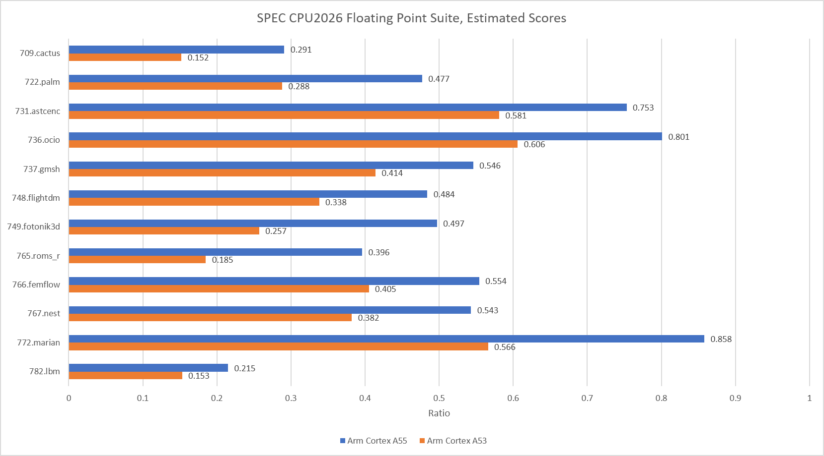
SPEC CPU2026’s floating point suite shows A55 pulling way ahead again, with a 50.45% geometric mean uplift over A53. I didn’t collect performance monitoring data for SPEC CPU2026 because each run takes such a long time on these low clocked, in-order cores. However, one thought is that SPEC CPU2026’s larger instruction footprints in its integer suite punish A55. Instruction cache misses tend to be less common in SPEC’s floating point workloads, which shifts emphasis back to A55’s superior memory subsystem.
Final Words
A55’s core architecture isn’t exciting, because it leaves most of A53’s framework unchanged. Arm made a sensible choice, because in-order cores do poorly at maintaining throughput around anything that takes more than a few cycles. Better branch prediction and caching down common causes of delay-causing events, and contribute directly to performance improvements.
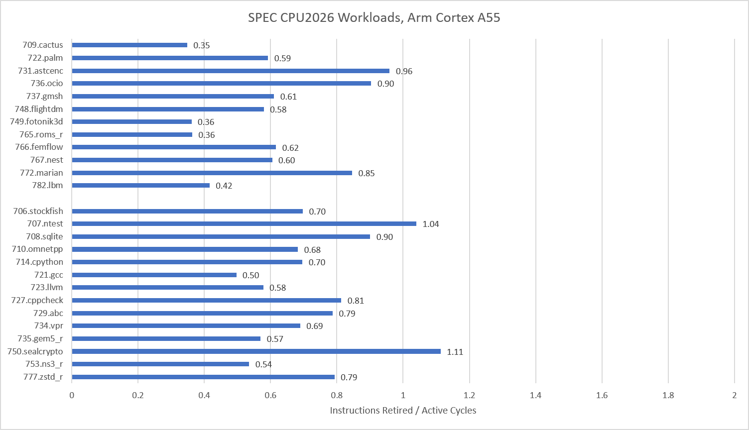
Even with better branch prediction and caching, A55’s IPC figures show the difficulty of feeding a 2-wide pipeline with in-order execution. Certainly there’s more room to push on the same fronts that Arm did with A55. Larger and faster caches could further mitigate backend memory stalls. More sophisticated branch prediction would help mitigate instruction side stalls.
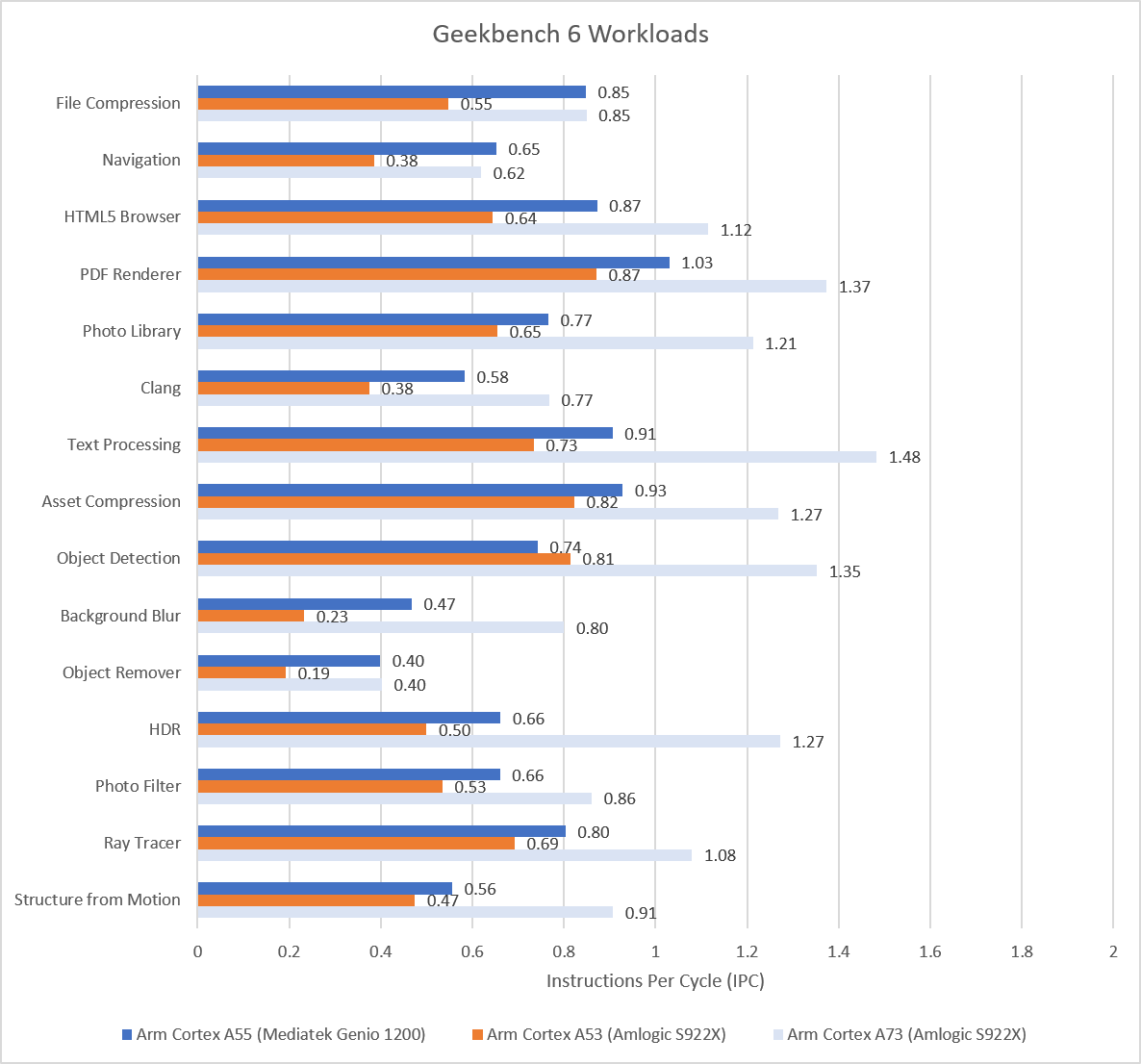
However, there’s likely a point where out-of-order execution starts to make sense even for sub-1W power targets. Larger caches take area and power. Branch prediction involves caching branch targets and outcomes, and runs into diminishing returns for increasing storage investment. Arm’s own A73 is a small 2-wide out-of-order design, and has no trouble pulling well ahead of A55 even without a clear memory subsystem advantage. For reference, A73 uses a pre-DSU system level setup, and has a 1 MB L2 cache in the Amlogic S922X.
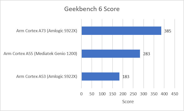
Arm ultimately decided in-order execution still has legs. They followed up A55 with the A510, which implements 3-wide in-order execution and uses shared components in dual core clusters to save area. I can’t imagine feeding a 3-wide core with in-order execution is any easier. But I guess for now, out-of-order execution is still too complex to pull off at sub-1W targets, even with modern process nodes.
As number of asset, constraint, and market parameters increase, classical portfolio optimization models becomes quite complicated to solve. Financial institutions should manage multiple objectives such as expected return, risk and return, liquidity, cost of trading, regulations, and ESG preferences under uncertain markets. Therefore the problem is a multi-objective optimization one.
Quantum-enhanced portfolio optimization is the combination of artificial intelligence (AI), classical high-performance computing (HPC), and quantum optimization algorithms that can help explore larger solution spaces faster for some optimization problem classes.
Quantum is expected to augment the AI tools, rather than replace them as a supplement for the high computationally demanding optimization problems when quantum computers become a mature technology. Core Capabilities: Portfolio Optimization, Risk management, Capital Allocation, Trading Optimization, and derivative portfolio optimization. The Benefits of Quantum Enhanced portfolio Optimization: Better exploration in the complexity space. Managing complex portfolio sizes.
Faster portfolio scenario analysis and estimation.
Improve portfolio rebalancing capabilities and adaptability with AI. Potential speed benefits on certain optimization and simulation tasks (once fault tolerant QCs are ready). Limitations: Noise in the systems, immature quantum hardware.
Application that utilize the current QCs only with limitations for the financial use case, or require robust fault tolerant QCs. Financial specific workflows, governance and regulatory compliance needs integration, explainable AI in order to increase trust in predictions for the use case. Market and asset price predictions are expected to work better from AI not QCs.
Strategic Vision: The future will be around hybrid intelligence.
Standard classical compute will dominate most of the standard analyses and transactions. The new era with the usage of AI will bring deeper insights and the capability to adapt to market volatility, and QCs will help augment computing capability for specific computationally challenging parts of the portfolio optimization and simulation processes when becoming mature. Financial Institutions that invest early with the appropriate tools (QCs aware algorithms, AI Analytics, a better computed infrastructure, governance) will be ready to take benefit from the future quantum enabled world.
Another interesting deep dive! That statement at the end ..."for now, out-of-order execution is still too complex to pull off at sub-1W targets, even with modern process nodes." brought up this question: What is the approximate power envelope of Apple's efficiency cores? Those have been out-of-order designs for several generations.