
Arm’s Bifrost Architecture and the Mali-G52

Arm (the company) is best known for its Cortex CPU line. But Arm today has expanded to offer a variety of licensable IP blocks, ranging from interconnects to IOMMUs to GPUs. GPUs make for an interesting discussion topic because they’ve evolved to become highly programmable and complex components, much like CPUs. Like CPU performance, GPU performance is highly visible to users, and forms an important part of a device’s specifications.
Arm Mali GPUs target low power and embedded devices, a characteristic shared with Arm’s Cortex CPUs. As a GPU, Mali tackles the same fundamental problems as high performance discrete GPUs that gamers and PC enthusiasts are familiar with. Graphics processing has plenty of inherent parallelism; it maps well to hardware that can track a lot of parallel work, and map it to a wide array of execution units. However, power and area constraints force a delicate approach to exploiting parallelism. A low-end laptop GPU may have at most a dozen watts to work with; anything above 6W will likely be unsustainable in a cell phone or tablet. Die area constraints are similarly tight, because an iGPU has to share a small die alongside a CPU and numerous accelerator blocks.
In another difference from AMD, Intel, and Nvidia GPUs, Mali is licensed out as a standalone IP block; Arm does not control the chip design process. Instead, implementers buy Arm IP and bring together a wide variety of other IP blocks to meet their chip-level goals. This business model makes Mali peculiar in the GPU space. Mali only handles 3D rendering and parallel compute, doesn’t provide hardware acceleration for video codecs, and can’t even drive a display by itself. A PC enthusiast expects this functionality to come with any GPU. However, excluding it from the Mali package lets implementers pick and choose video and display engines to meet their needs. Hypothetically, an implementer could even go without video and display engines, and use Mali purely as compute accelerator. Lack of control over the chip design process creates further challenges: Mali has to perform well across the widest possible range of use cases to increase Arm’s customer base, yet Arm has to do so with no control over the all-important chip-level memory subsystem.
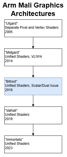
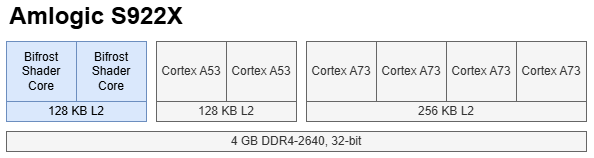
Bifrost is Arm’s second generation unified shader architecture from around 2016. It comes after Midgard, which brought unified shaders to Mali well after AMD, Intel, and Nvidia did so for their GPU lines. For this article I’ll use data from the Mali-G52, as implemented in the Amlogic S922X. The Mali-G52 is a very small GPU, so I’ll also use comparison data from Qualcomm’s Adreno 615, as implemented in the Snapdragon 670.
Software APIs
GPU programming interfaces saw enormous change in the late 2000s and early 2010s. Graphics APIs moved to a unified shader model, where different shader stages run on the same execution pipelines. GPU compute rose quickly as those execution pipelines became increasingly flexible. Arm’s Midgard got onboard the programmability train with OpenGL ES 3.0, Vulkan, and OpenCL 1.1 support. While Midgard could handle modern APIs, its VLIW4 setup had brittle performance characteristics. Arm’s compiler could be hard pressed to extract enough instruction level parallelism to fill a VLIW4 bundle, especially with compute code. Even in graphics code, Arm noted that 3-wide vectors were very common and could leave one VLIW4 component unused.
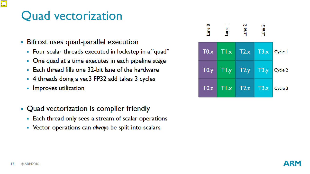
Bifrost switches to a scalar, dual issue execution model to address Midgard’s shortcomings. From a single thread’s point of view, registers are now 32-bits wide rather than 4×32-bit vectors. Instead of having one thread issue operations to fill four FP32 lanes, Bifrost relies on multiple API threads to fill an Execution Engine’s four or eight lanes. A lane in Bifrost feeds both a FMA and FADD execution pipeline, so Bifrost still benefits from instruction level parallelism. However, packing two operations into an instruction should be easier than four. As a result, Arm hopes to achieve more consistent performance with a simpler compiler.
Arm’s move from SIMD to scalar execution within each API thread with Bifrost parallels AMD’s Terascale to GCN transition, aiming for more consistent performance across compute workloads.
GPU Organization
Midgard and Bifrost may be vastly different at the execution pipeline level, but the two share a similar high level organization. Bifrost Execution Engines (EEs) contain execution pipelines and register files, and act as a replacement for Midgard’s arithmetic pipelines. Looking outside Arm, EEs are the rough equivalent of Intel Execution Units (EUs) or AMD SIMDs.
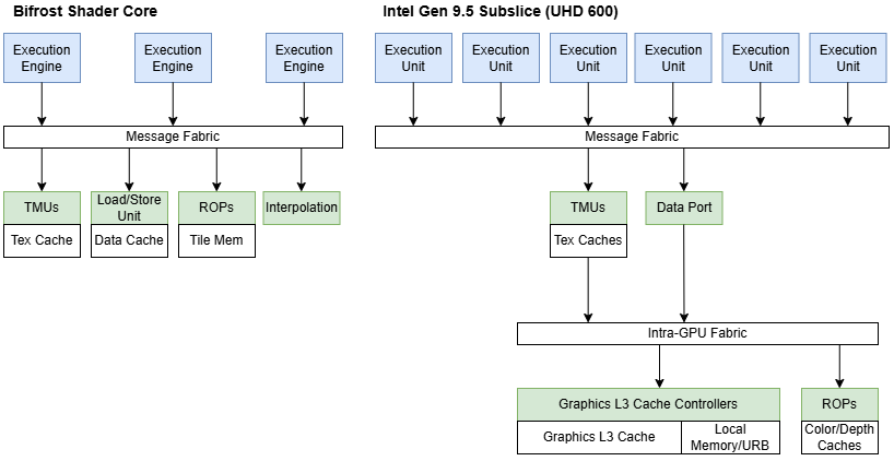
Multiple EEs live in a Shader Core (SC). A messaging fabric internal to the Shader Core links EEs to memory pipelines and other shared fixed function hardware. A SC’s texture and load/store units include first level caches, making them a close equivalent to Intel’s subslices, AMD’s CUs or WGPs, or Nvidia’s SMs. One difference is that Bifrost places pixel backends (ROPs) at the Shader Core level, while desktop GPU architectures place them at a higher level subdivision. Bifrost doesn’t have another subdivision level beyond the Shader Core.
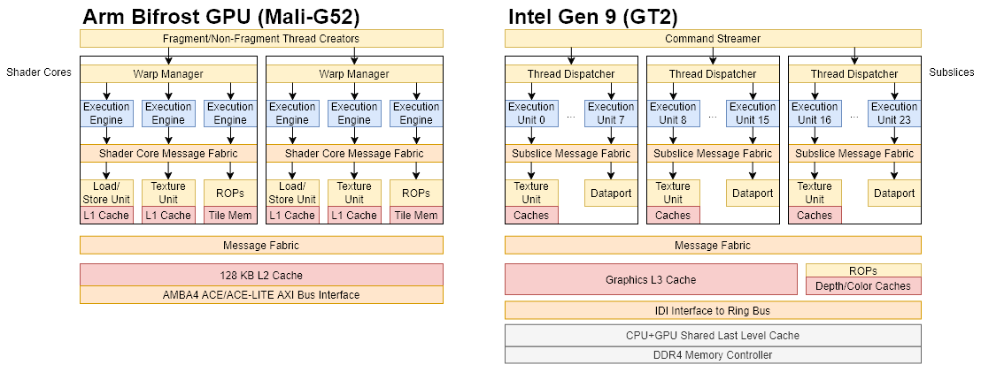
A defining Mali characteristic is an extraordinary number of levers for tuning GPU size. Besides adjusting Shader Core count, Arm can adjust a Shader Core’s EE count, cache sizes, and ROP/TMU throughput.
Flexibility extends to the EEs, which can operate on 4- or 8-wide warps, with correspondingly wide execution pipelines. Arm can therefore finely adjust GPU size in multiple dimensions to precisely target performance, power, and area goals. By comparison, AMD and Nvidia generally use the same WGP/SM structure, from integrated GPUs all the way to 300W+ monsters.
Bifrost can theoretically scale to 32 Shader Cores. Doing so with triple-EE SCs would provide 1.23 TFLOPS of FP32 FMA performanec at 800 MHz, which is in the same ballpark as Intel’s largest Skylake GT4e configuration. It’s not high power or high performance by discrete GPU standards, but well above what would fit in an average cell phone or tablet. The Mali-G52 in the Amlogic S922X is a small Bifrost configuration, with two triple-EE SCs running at 800 MHz, each EE 8-wide. Qualcomm’s Adreno can scale by varying Shader Processor count and uSPTP size. Adreno 6xx’s execution unit partitions are much larger at either 64- or 128-wide.
Shader Cores across a Bifrost GPU share a L2 cache. A standard ACE memory bus connects Bifrost to the rest of the system, and Arm’s influence ends at that point.
Shader Frontend
Bifrost’s instruction cache capacity hasn’t been disclosed, but instruction throughput is highest in a loop with 512 or fewer FP adds; as the loop body exceeds 1280 FP adds, instruction throughput takes another dip. Bifrost uses 78-bit instructions, which specify two operations corresponding to the FMA and FADD pipes. Arm’s compiler can issue FP adds down both pipes. Compiled binary size increases by 6-7 bytes for each FP add statement, with FMA+FADD packing decreasing size and clause/quadword header adding overhead. Based on binary size increase over a baseline, instruction cache capacity is possibly around 8 KB, which would put it in line with Qualcomm’s Adreno 6xx.
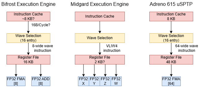
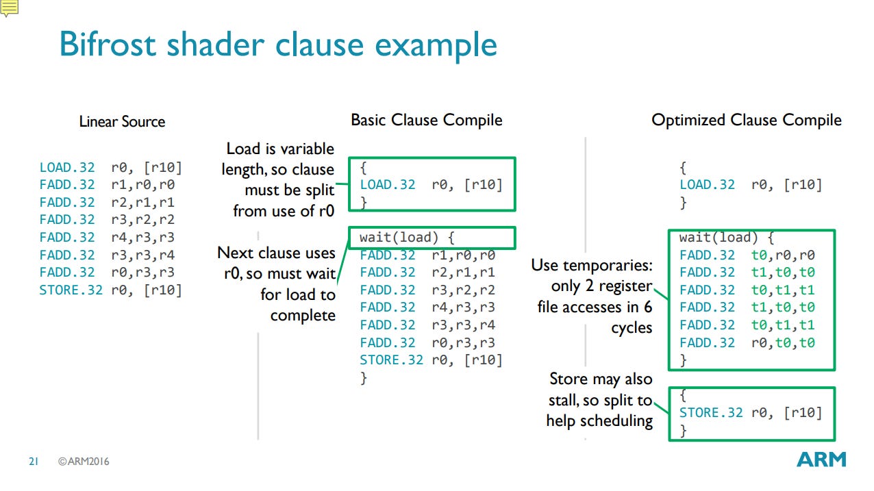
Each Execution Engine tracks state for up to 16 warps, each of which corresponds to a vector of eight API threads executing in lockstep. Hardware switches between warps to hide latency, much like SMT on a CPU. Bifrost uses a clause-based ISA to simplify scheduling. Instructions packed into a clause execute atomically, and architectural state is only well-defined between clauses. Only one instruction in a clause can access long- and variable-latency units outside the EU, such as memory pipelines.
Memory dependencies are managed between clauses, so an instruction that needs data from a memory access must go into a separate clause. A 6-entry software managed scoreboard specifies cross-clause dependencies. Clauses reduce pressure on scheduling hardware, which only has to consult the scoreboard at clause boundaries rather than with each instruction. Bifrost has parallels to AMD’s Terascale, which also uses clauses, though their implementation details differ. Terascale groups instructions into clauses based on type; for example, math instructions go into an ALU clause, and memory accesses go into separate texture- or vertex-fetch clauses.
From a programmer’s perspective, Mali-G52 can theoretically have 768 active workitems across the GPU; that’s eight lanes per warp * 16 warps per EE * 6 EEs across the GPU. In practice, actual active thread count, or occupancy, can vary depending on available parallelism and register usage; Bifrost’s ISA provides up to 64 registers, but using more than 32 will halve theoretical occupancy (implying 16 KB of register file capacity). There are no intermediate allocation steps. For comparison, Qualcomm’s Adreno 6xx can only achieve maximum occupancy with 12 registers per thread.
Register Access and Execution Pipelines
Instruction execution is split into register access, FMA, and FADD stages. During the register access stage, a Bifrost instruction takes direct control of the operand collector to read instruction inputs and write results from the prior instruction. Each EE’s register file has four ports; two can handle reads, one can handle writes, and one can handle either. Feeding the EE’s FMA and FADD pipes would nominally require five inputs, so register read bandwidth is very limited. If a prior instruction wants to write results from both the FMA and FADD pipes, register bandwidth constraints only become more severe.
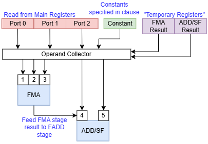
To alleviate register file bandwidth demands, Bifrost can source inputs from a uniform/constant port, which provides 1×64 bits or 2×32 bits of data from immediate values embedded into a clause. Additionally, Bifrost provides “temporary registers”, which are really software-controlled forwarding paths that hold results from the prior instruction. Finally, because the FADD unit is placed at a later pipeline stage than the FMA unit, the FADD unit can use the FMA unit’s result as an input.
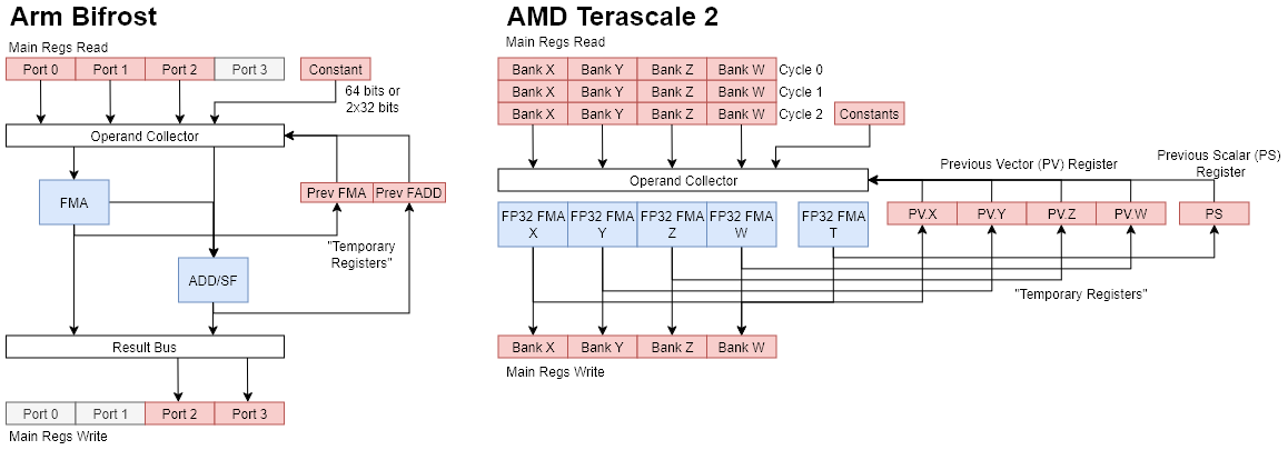
Bifrost’s temporary registers, software-managed operand collector, and register bandwidth constraints will be immediately familiar to enjoyers of AMD’s Terascale 2 architecture. Terascale 2 uses 12 register file inputs to feed five VLIW lanes, which could need up to 15 inputs. Just like Bifrost, AMD’s compiler uses a combination of register reuse, temporary registers (PV/PS), and constant reads to keep the execution units fed. Like Bifrost, PV/PS are only valid between consecutive instructions in the same clause, and reduce both register bandwidth and allocation requirements. One difference is that result writeback on Terascale 2 doesn’t share register file bandwidth with reads, so using temporary registers isn’t as critical.
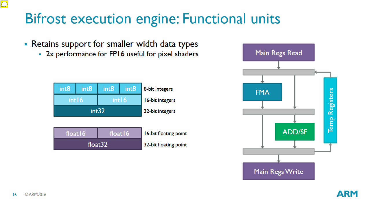
Bifrost’s execution pipelines have impressive flexibility when handling different data types and essentially maintain 256-bit vector execution (or 128-bit on 4-wide EE variants) with 32/16/8-bit data types. Machine learning research was already well underway in the years leading up to Bifrost, and rather than going all-in as Nvidia did with Volta’s dedicated matrix multiplication units, Arm made sure the vector execution units could scale throughput with lower-precision types.
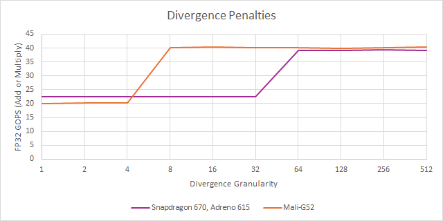
Qualcomm’s Adreno 615 takes a different execution strategy, with 64-wide warps and correspondingly wide execution units. That makes Adreno 615 more prone to divergence penalties, but lets Qualcomm control more parallel execution units with one instruction. Adreno 615 has 128 FP32 lanes across the GPU, all capable of multiply-adds, and runs them at a very low 430 MHz. Mali-G52 can only do 48 FP32 FMA operations per clock, but can complete 96 FP32 operations per clock with FMA+FADD dual issue. Combined with a higher 800 MHz clock speed, Mali-G52 can provide similar FP add throughput to Adreno 615. However, Adreno 615 fares better with multiply-adds, and can reach just over 100 GFLOPS.
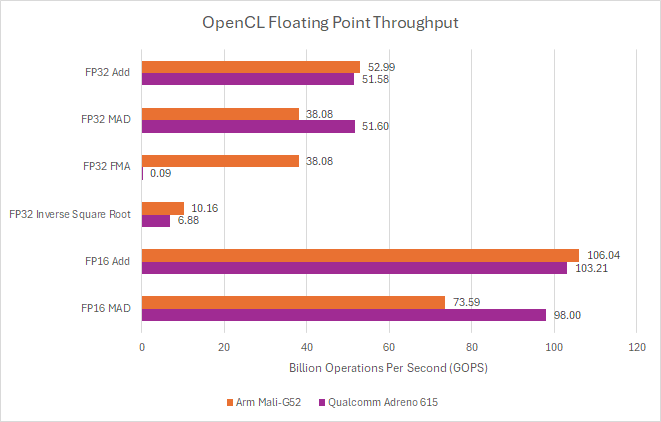
I’m being specific by saying multiply-adds, not fused multiply-adds; the latter rounds only once after the multiply and add (both computed with higher intermediate precision), which improves accuracy. Adreno apparently has no fast-path FMA hardware, and demanding FMA accuracy (via OpenCL’s fma function) requires over 600 cycles per FMA per warp. Bifrost handles FMA with no issues. Both mobile GPUs shine with FP16, which executes at double rate compared to FP32.
Special functions like inverse square roots execute down Bifrost’s FADD pipeline, at half rate compared to basic operations (or quarter rate if considering FMA+FADD dual issue). Arm has optimized handling for such complex operations on Bifrost compared to Midgard. Only the most common built-in functions exposed in APIs like OpenCL get handled with a single instruction. More complex special operations take multiple instructions. Adreno executes special functions at a lower 1/8 rate.
Integer operations see a similar split on Bifrost as FP ones. Integer adds can execute down the FADD pipe, while multiplies use the FMA pipe. Adreno’s more uniform setup gives it an advantage for adds; both of Bifrost’s pipes can handle integer operations at full rate, giving Bifrost an advantage for integer multiplies.
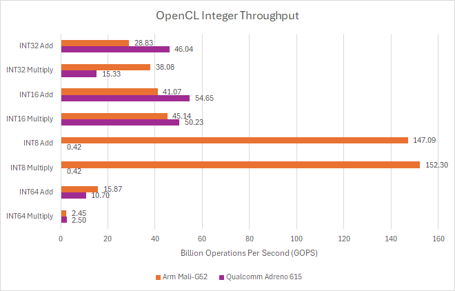
Lower precision INT8 operations see excellent throughput on Bifrost, but suffer glass jaw behavior on Adreno. Clearly Qualcomm didn’t implement fast-path INT8 hardware, but an INT8 operation can be carried out on INT32 units with the result masked to 8 bits. Terascale 2 also lacks INT8 hardware, but can emulate them at just under half rate. FP64 support is absent on both mobile GPUs.
Bifrost’s execution engines are built for maximum flexibility, and handle a wider range of operations with decent performance than Qualcomm’s Adreno. Adreno, by comparison, appears tightly optimized for graphics. Graphics rasterization doesn’t need higher precision from fused multiply-adds, nor do they need lower precision INT8 operations. Qualcomm packs a variety of other accelerators onto Snapdragon chips, which could explain why they don’t feel the need for consistently high GPU performance across such a wide range of use cases. Arm’s licensing business model means they can’t rely on the chip including other accelerators, and Bifrost’s design reflects that.
Memory Pipeline
Bifrost’s memory subsystem includes separate texture and load/store paths, each with their own caches. EEs access these memory pipelines through the Shader Core’s messaging network. Intel uses similar terminology, with EUs accessing memory by sending messages across the subslice’s internal messaging fabric. AMD’s CUs/WGPs and Nvidia’s SMs have some sort of interconnect to link execution unit partitions to shared memory pipelines; Arm and Intel’s intra-core networks may be more flexible still, since they allow for variable numbers of execution unit partitions:
Arm’s documentation states Mali-G52’s load/store cache and texture caches are both 16 KB. However, latency testing suggests the texture cache is 8 KB. These parameters may be configurable on implementer request, and indeed vary across different Bifrost SKUs. For example, Mali-G71, a first-generation Bifrost variant, has 16 KB and 8 KB load/store and texture caches respectively on the spec sheet.
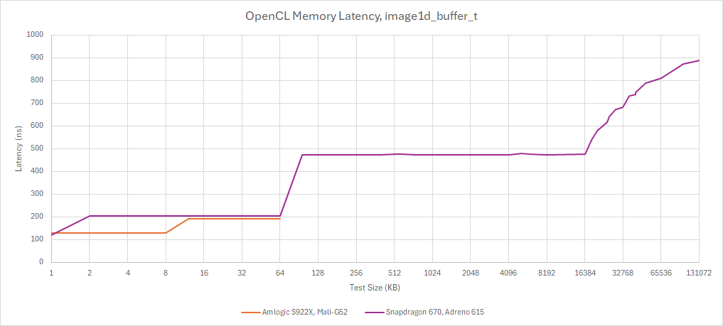
Pointer chasing in the texture cache carries slightly higher latency than doing so in the load/store cache, which isn’t surprising. However it’s worth noting some GPUs, like AMD’s Terascale, have TMUs that can carry out indexed addressing faster than doing the same calculation in the programmable shader execution units.
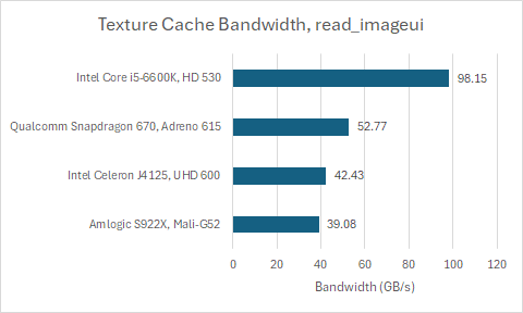
Texture cache bandwidth is low on Bifrost compared to Adreno and Intel’s Gen 9. OpenCL’s read_imageui function returns a vector four 32-bit integers, which can be counted as a sample of sorts. Mali-G52 can deliver 26.05 bytes per Shader Core cycle via read_imageui, consistent with Arm’s documentation which states a large Shader Core variant can do two samples per clock. Adreno 615 achieves 61.3 bytes per uSPTP cycle, or four samples. That’s enough to put Adreno 615 ahead despite its low clock speed. I suppose Qualcomm decided to optimize Adreno’s texture pipeline for throughput rather than caching capacity, because its 1 KB texture cache is small by any standard.
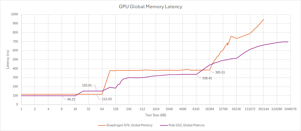
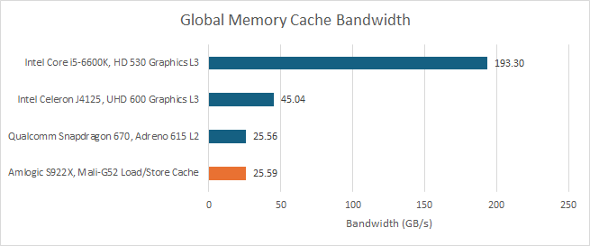
It’s amazing how little cache bandwidth these mobile GPUs have. Even on the same chip, the Amlogic S922X’s four A73 cores can hit 120 GB/s of L1D read bandwidth. Global memory bandwidth for compute applications is similarly limited. Adreno 615 and Mali-G52 are about evenly matched. A Bifrost SC delivered 16 bytes per cycle in a global memory bandwidth test, while an Adreno 615 uSPTP can load 32 bytes per cycle from L2.
Bifrost’s L1 can likely deliver 32 bytes per cycle, matching the texture cache, because I can get that from local memory using float4 loads. I don’t have a float4 version of my global memory bandwidth test written yet, but results from testing local memory should suffice:
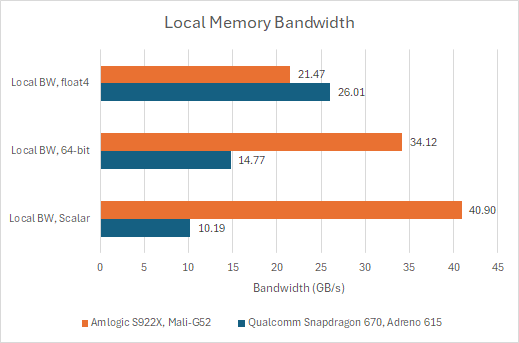
Bifrost metaphorically drops local memory on the ground. GPU programming APIs provide a workgroup-local memory space, called local memory in OpenCL or Shared Memory in Vulkan. GPU hardware usually backs this with dedicated on-chip storage. Examples include AMD’s Local Data Share, and Nvidia/Intel reserving a portion of cache to use as local memory.
Mali GPUs do not implement dedicated on-chip shared memory for compute shaders; shared memory is simply system RAM backed by the load-store cache just like any other memory type
Bifrost doesn’t give local memory any special treatment. An OpenCL kernel can allocate up to 32 KB of local memory, but accesses to local memory aren’t guaranteed to remain on-chip. Worse, each Shader Core can only have one workgroup with local memory allocated, even if that workgroup doesn’t need all 32 KB.

GPUs that back local memory with on-chip storage can achieve better latency than Bifrost; that includes Adreno. Qualcomm disclosed that Adreno X1 allocates local memory out of GMEM, and their prior Adreno architectures likely did the same. However, Qualcomm doesn’t necessarily enjoy a bandwidth advantage, because GMEM access similarly appears limited to 32 bytes per cycle.
L2 Cache and System Level
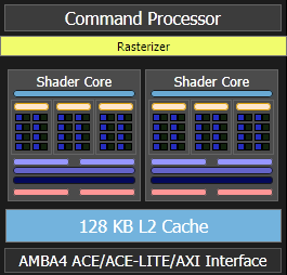
Bifrost’s L2 functionally works like the L2 cache in modern AMD and Nvidia GPUs. It’s a write-back cache built from multiple slices for scalability. Arm expects Bifrost implementations to have 64-128 KB of L2 per Shader Core, up from Midgard’s corresponding 32-64 KB figure. Amlogic has chosen the lower end option, so the Mali-G52 has 128 KB of L2. A hypothetical 32 Shader Core Bifrost GPU may have 2-4 MB of L2.
On the Amlogic S922X, L2 latency from the texture side is slightly better than on Qualcomm’s Adreno 615. However, Adreno 615 enjoys better L2 latency for global memory accesses, because it doesn’t need to check L1 on the way. L2 bandwidth appears somewhat lower than Adreno 615, though Mali-G52 has twice as much L2 capacity at 128 KB. However the Snapdragon 670 has a 1 MB system level cache, which likely mitigates the downsides of a smaller GPU-side L2.

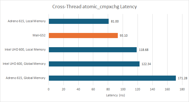
Bifrost shows reasonably good latency when using atomic compare and exchange operations to pass data between threads. It’s faster than Adreno 615 when using global memory, though Qualcomm offers lower latency if you use atomics on local memory.
GPUs often handle atomic operations using dedicated ALUs close to L2 or backing storage for local memory. Throughput for INT32 atomic adds isn’t great compared to Intel, and is very low next to contemporary discrete GPUs from AMD and Nvidia.

L2 misses head out to the on-chip network, and make their way to the DRAM controller. Amlogic has chosen a a 32-bit DDR4-2640 interface for the S922X, which provides 10.56 GB/s of theoretical bandwidth. A chip’s system level architecture is ultimately up to the implementer, not Arm, which can affect Bifrost’s system level feature support.
In alignment with Bifrost’s compute aspirations, Arm designed a L2 that can accept incoming snoops. With a compatible on-chip interconnect and CPU complex, Bifrost can support OpenCL Shared Virtual Memory with fine-grained buffer sharing. That lets the CPU and GPU share data without explicit copying or map/unmap operations. Evidently Amlogic’s setup isn’t compatible, and Mali-G52 only supports coarse-grained buffer sharing. Worse, it appears to copy entire buffers under the hood with map/unmap operations.
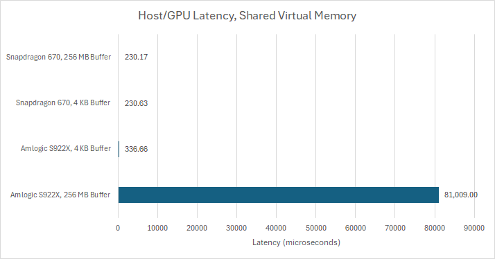
Qualcomm on the other hand controls chip design from start to finish; Adreno 615 supports zero-copy behavior, and Qualcomm’s on-chip network has the features needed to make that happen.
While many modern GPUs can support zero-copy data sharing with the CPU, copy performance can still matter. Besides acting as a baseline way of getting data to the GPU and retrieving results, buffers can be de-allocated or reused once their data is copied to the GPU. Copy bandwidth between the host and GPU is low on the Amlogic S922X at just above 2 GB/s. A copy requires both a read and a write, so that would be 4 GB/s of bandwidth. That’s in line with measured global memory bandwidth above, and suggests the DMA units aren’t any better than the shader array when it comes to accessing DRAM bandwidth.

Adreno 615 has better copy performance, possibly helped by its faster LPDDR4X DRAM interface. However, copying data back from the GPU is agonizingly slow. Games largely transfer data to the GPU, not the other way around, so that’s another sign that Adreno is tightly optimized for gaming.
Rasterization and Tiled Rendering
Adreno and Mali share another common problem: mobile devices can’t afford high bandwidth DRAM interfaces compared to desktop CPUs, let alone GPUs with wide GDDR setups. However, graphics rasterization can be bandwidth-hungry, and ROPs can be a significant source of bandwidth pressure. When pixel/fragment shaders output pixel colors to the ROPs, the ROPs have to ensure those results are written in the correct order. That can involve depth testing or alpha blending, as specified by the application.

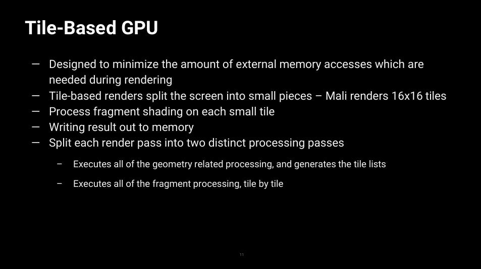
Both Adreno 6xx and Bifrost reduce ROP-side DRAM traffic using tiled rendering, which splits the screen into rectangular tiles, and renders them one at a time. Tiles are sized to fit within on-chip buffers, which contain intermediate accesses from alpha blending and depth testing. The tile is only written out to DRAM after it’s finished rendering. Tiled rendering requires building per-tile visible triangle lists as vertex shaders finish calculating vertex coordinates. Then, those triangle lists are read back as the GPU rasterizes tiles one by one. Handling triangle lists generates DRAM traffic, which could obviate the benefit of tiled rendering if not handled carefully.
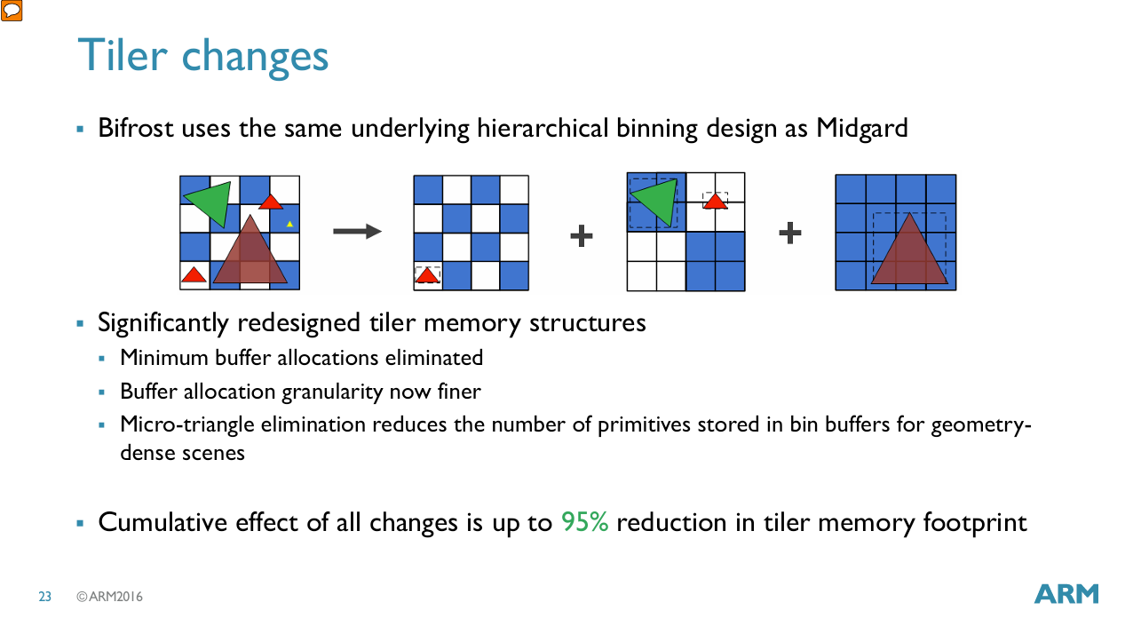
Bifrost uses a hierarchical tiling strategy like Midgard. Tiles are nominally 16×16 pixels, but Arm can use larger power-of-two tile sizes to try containing triangles. Doing so reduces how often a triangle overlaps different tiles and thus is referenced in multiple triangle lists. Compared to Midgard, Arm also redesigned tiler memory structures with finer-grained allocations and no minimum buffer allocations. Finally, Bifrost can eliminate triangles too small to affect pixel output at the tiler stage, which also reduces wasted pixel/fragment shader work. These optimizations can reduce both bandwidth usage and memory footprint between the vertex and pixel shader stages. Arm also optimizes bandwidth usage at the tile writeback stage, where “Transaction Elimination” compares a tile’s CRC with the corresponding tile in the prior frame, and skips tile writeback if they match, an often efficient trade of logic for memory bus usage.
Because Bifrost uses 256 bits of tile storage per pixel, tile memory likely has at least 8 KB of capacity. Arm further implies tile memory is attached to each Shader Core, so Mali-G52 may have 16 KB of tile memory across its two Shader Cores. Adreno 615 also uses tiled rendering, and uses 512 KB of tile memory (called GMEM) to hold intermediate tile state.
Compute Performance: FluidX3D
FluidX3D is a GPGPU compute application that simulates fluid behavior. FP16S/FP16C modes help reduce DRAM bandwidth requirements by using 16-bit FP formats for storage. Calculations are still performed on FP32 values to maintain accuracy, with extra instructions used to convert between 16 and 32-bit FP formats.

Adreno 615 and Mali-G52 both appear more compute-bound than bandwidth-bound, so FP16 formats don’t help. FluidX3D uses FMA operations by default, which destroys Adreno 615’s performance because it doesn’t have fast-path FMA hardware. Qualcomm does better if FMA operations are replaced by multiply-adds. However, Adreno 615 still turns in an unimpressive result. Despite having more FP32 throughput and more memory bandwidth on paper, it falls behind Mali-G52.
Power Management
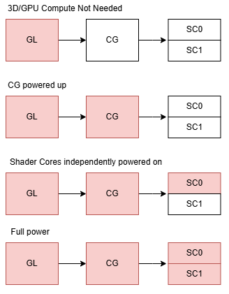
Mali-G52 is organized into four power domains. A “GL” domain is always on, and likely lets the GPU listen for power-on commands. Next, a “CG” (Common Graphics?) domain is powered on when the GPU needs to handle 3D work or parallel compute. Next, the Shader Cores (SC0, SC1) are powered on as necessary. Each Shader Core sits on a separate power domain, letting the driver partially power up Mali’s shader array for very light tasks.
Power savings can also come from adjusting clock speed. The Amlogic S922X appears to generate Mali-G52’s clocks from 2 GHz “FCLK”, using various divider settings.

Final Words
Arm’s business model relies on making its IP blocks attractive to the widest possible variety of implementers. Bifrost fits into that business model thanks to its highly parameterized design and very small building blocks, which makes it ideal for hitting very specific power, area, and performance levels within the low power iGPU segment.

Qualcomm’s Adreno targets similar devices, but uses much larger building blocks. Adreno’s strategy is better suited to scaling up the architecture, which aligns with Qualcomm’s ambition to break into the laptop segment. However, larger building blocks make it more difficult to create tiny GPUs. I feel like Qualcomm scaled down Adreno 6xx with all the knobs they had, then had to cut clock speed to an incredibly low 430 MHz to hit the Snapdragon 670’s design goals.
Beyond scaling flexibility, Bifrost widens Arm’s market by aiming for consistent performance across a wide range of workloads. That applies both in comparison to Qualcomm’s Adreno, as well as Arm’s prior Midgard architecture. Bifrost’s execution units are pleasantly free of “glass jaw” performance characteristics, and GPU to CPU copy bandwidth is better than on Adreno. Adreno isn’t marketed as a standalone block, and is more sharply focused on graphics rasterization. Qualcomm might expect common mobile compute tasks to be offloaded to other blocks, such as their Hexagon DSP.
Overall, Bifrost is an interesting look into optimizing a low power GPU design to cover a wide range of applications. It has strong Terascale to GCN energy, though Bifrost really lands at a midpoint between those two extremes. It’s fascinating to see Terascale features like clause-based execution, a software-controlled operand collector, and temporary registers show up on a 2016 GPU architecture. Apparently features that Terascale used to pack teraflops of FP32 compute into 40nm class nodes continue to be useful for hitting very tight power targets on newer nodes. Since Bifrost, Arm has continued to modernize their GPU architecture with a focus on both graphics rasterization and general purpose compute. They’re a fascinating and unique GPU designer, and I look forward to seeing where they go in the future.
If you like the content then consider heading over to the Patreon or PayPal if you want to toss a few bucks to Chips and Cheese. Also consider joining the Discord.
Thanks for another great deep dive! The history of the Mali GPUs and how ARM came to having a GPU department and developing low-power GPU IP for mobile devices is fascinating all in itself. It started with ARM's acquisition of Falanx, located in Trondheim, Norway. Hence all those names from Norse mythology for the various generations.
It's IMHO really impressive that, at least in the smartphone space, current generation fully featured Malis (Immortalis) are very competitive with Qualcomm's current gen Adreno GPUs.