AmpereOne at Hot Chips 2024: Maximizing Density
Ampere Computing focuses on developing cloud-native processors, and aims to serve many users while providing security, privacy, and consistent performance, without relying on process node scaling. Features that increase performance at the expense of consistency were ruled out, including SMT and on-the-fly clock speed adjustments. Density is also a priority, in order to let cloud providers service as many customers as possible with each physical server.
AmpereOne is Ampere’s latest server CPU, and uses an in-house core design. That draws a clear contrast to Amazon’s Graviton 4, Nvidia’s Grace, or Ampere’s own last generation Altra CPU. All of those license Neoverse cores from Arm. Ampere’s custom core can run at up to 3.7 GHz. Oracle has made AmpereOne cloud instances publicly available in the weeks before Hot Chips, so I’ve been able to gather some data. I’ll be using that to provide context for Ampere’s presentation. Oracle’s cloud instances use a SKU that tops out at 3 GHz.
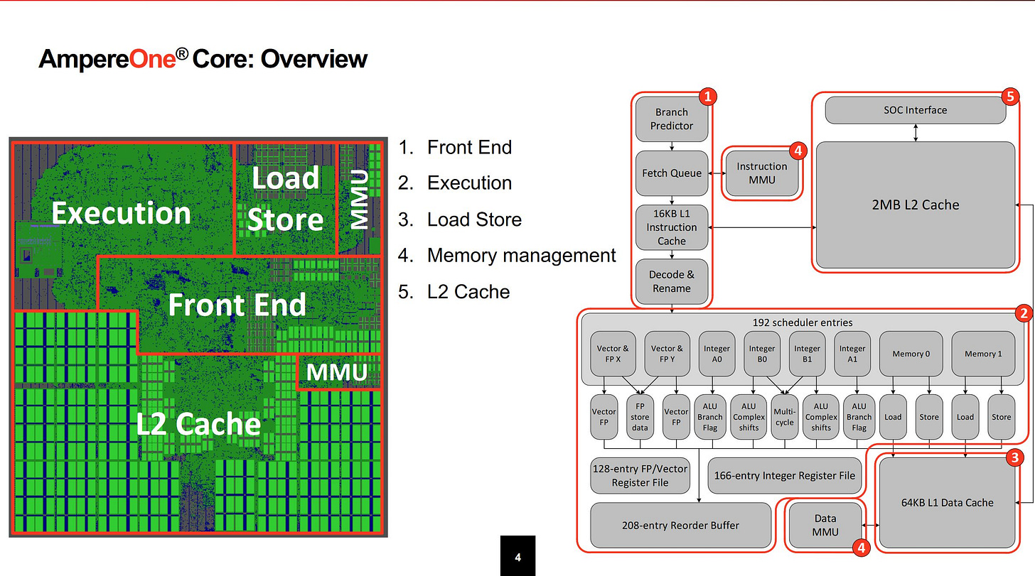
A GDS plot shows a large L2 cache, with core components clustered around the top. The L2 cache takes up considerable core area. One comparison is AMD’s Zen 4c core. AMD uses a smaller 1 MB L2 cache in combination with a lower latency L3. Zen 4 also has a wider pipeline, more reordering capacity, and substantial vector capabilities. Still, the L2 cache takes up quite a bit of area in AMD’s design.
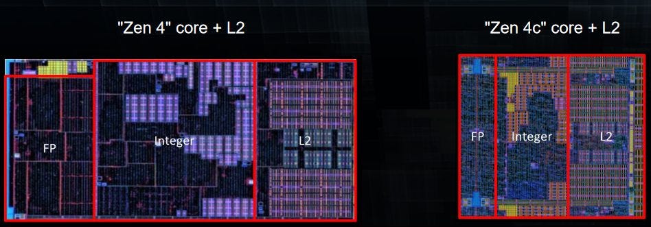
I wonder if this is a trait of density optimized cores. Perhaps L2 caches are quite dense even in high performance designs, so most of the gain in a density optimized design comes from shrinking core logic and L1 memories.
Frontend Design
The frontend is responsible for bringing instructions into the core. Branch prediction tells the frontend where to go, and is critical for both performance and power efficiency. Ampere uses an 8-table TAGE predictor for direction prediction. A TAGE predictor is pretty much state of the art, and can select the best history length (from a geometric series) to use for each branch. AmpereOne can choose one of eight tables to use to provide a prediction, with each table providing a prediction using a different history length. This is a state-of-the-art prediction technique also used by AMD, Qualcomm, and probably Intel.
Ampere claims prediction accuracy in the high 90% range, which is in line with other predictors in recent CPUs. From testing on an Oracle cloud instance, that claim generally seems accurate. Even a challenging workload like file compression enjoys over 95% branch prediction accuracy.
Mispredicts per instruction are roughly in-line with AMD’s latest cores, which is a good place to be. This metric takes executed instruction count differences into account.
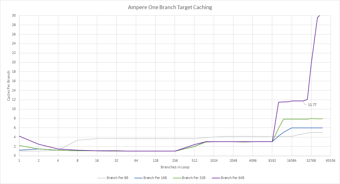
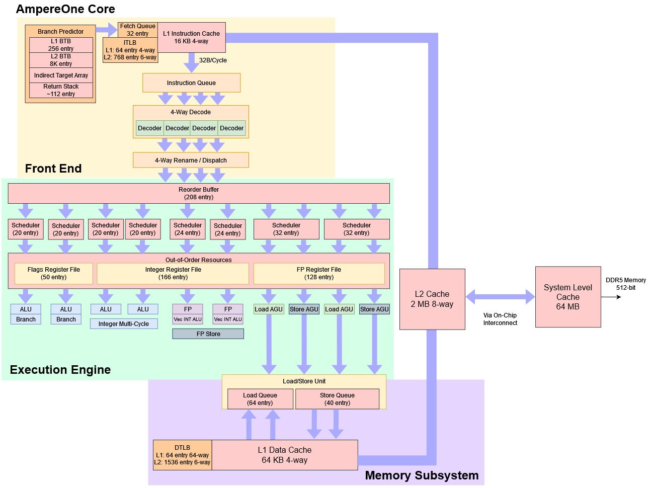
An 8K entry branch target buffer (BTB) tracks frequently used branch targets. The first level has 256 entries and zero-bubble latency from Ampere’s slides, which aligns with microbenchmarking results. The second level has 8K entries. I microbenchmarked using a chain of unconditional taken branches, and those see one branch every three cycles (2 cycle latency) once it spills out of the L1 BTB.
Branches that miss the L2 BTB appear to hit cache latency. If so, a code fetch from L2 has a latency of 11-12 cycles, which is similar to latency from the data side.
AmpereOne has a low 10 cycle mispredict recovery time. As part of the effort to achieve this low pipeline length, Ampere kept the instruction cache small at 16 KB. Since Ampere doesn’t use a micro-op cache or any faster source of instruction delivery, L1 instruction cache latency is part of the mispredict penalty. Therefore, using a smaller, lower latency instruction cache helps Ampere achieve a fast 10 cycle mispredict penalty. For comparison, Zen 4 has a 11 to 18 cycle mispredict penalty, with a claimed 13 cycle common case. The fastest 11 cycle case is likely for a micro-op cache hit. AmpereOne and Zen 4 have very different clock targets, but Ampere has achieved a very low mispredict recovery time in cycles.
The predictor is decoupled from the fetch pipeline by a 32 entry queue, which lets the branch predictor run ahead and drive instruction prefetch. Because the L1 instruction cache is small, Ampere implemented a low latency path from L2 to the frontend pipeline. L2 bandwidth to the frontend is sufficient to fully feed the decoders, and that aligns with a microbenchmark where I fill an array with NOPs with a return at the end, and jump to it.
This high L2 code fetch performance is important because the small L1 instruction cache from testing can behave closer to a micro-op cache depending on the application. Instructions should be fetched from the 16 KB L1i most of the time, just as Zen 4/5 do so from their micro-op caches most of the time. However, streaming code from L2 (or L1i in Zen 4/5’s case) needs to provide sufficient performance to not drop the ball with large code footprints.

The decode stage on AmpereOne can emit four micro-ops per cycle, but those can come from up to five instructions per cycle. That ability to scan five instructions per cycle helps exploit instruction fusion cases, where two adjacent instructions can be combined into one micro-op. Micro-op fusion means instructions can be tracked with fewer slots consumed in backend resources, and is also a goal pursued by Intel, AMD, Arm, and Qualcomm. Ampere says they believe they have the most aggressive fusing in the industry, allowing for high throughput from a 4-wide machine.
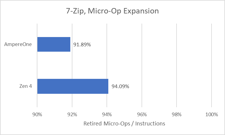
From brief testing, file compression is an interesting workload for instruction fusion. it has a lot of branches, and many CPUs can fuse a flag setting instruction with an adjacent conditional branch. Both Zen 4 and AmpereOne achieve negative micro-op expansion, which makes more efficient use of downstream queues and buffers.
AmpereOne’s frontend design is unconventional with its small instruction cache size. Ampere said they decided to size frontend structures in order to aggressively cut down on frontend latency and deliver instructions to the execution units as fast as possible. They evaluated over 1000 instruction traces to inform their design and tradeoffs.
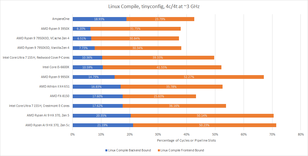
From a quick look at three workloads alongside data from a prior article, Ampere’s custom core is not more frontend bound than other cores.
A close comparison is Crestmont, which also tends to be far more backend bound than frontend bound. Crestmont is also density optimized, but uses a 64 KB instruction cache to feed a 6-wide decoder.
A complicating factor is that AmpereOne (and Crestmont) tend to be more backend bound than high performance designs like Zen 4. Still, that at least means AmpereOne’s slightly unconventional frontend caching strategy isn’t holding back performance.
Backend Execution Engine
At the backend, AmpereOne has eight schedulers feeding 12 execution pipes. Ampere says they’ve implemented “particularly” deep schedulers with 192 total entries. There are four integer schedulers, letting the core handle two branches and two complex shifts per cycle. Two of those schedulers can issue multi-cycle integer operations like multiplies and divides to a shared unit. From microbenchmarking using Henry Wong’s methodology, the integer schedulers are 20 entries deep.
On the floating point side, microbenchmarking indicates there are two schedulers with about 24 entries. Basic FP instructions like floating point adds can use both schedulers and their associated port. Both ports can also handle BF16, FP16, and AES operations. Less common instructions like ADDV and FJCVTZS are only implemented on one port. Both ports can feed a shared FP store data unit.
AmpereOne has two schedulers for memory operations, which support all addressing modes and can each pick one load and one store per cycle. Microbenchmarking indicates each memory scheduler has 32 entries.
Tuning distributed schedulers can be difficult because one queue filling up can cause a dispatch stall at the renamer, even if entries in other queues are free. On a file compression workload that I tested, micro-ops may be inefficiently distributed across the four schedulers/pipes. Alternatively the core could be running out of space in integer register file, and that increments the same performance monitoring event (IDR_STALL_IXU_SCHED). I’ll need to test the core more to see which is the case.
But I suspect micro-ops are not well distributed across ports in the file compression workload because one of the integer issue queues, designated IXA in performance monitoring documentation, saw very high load compared to the others.
7-Zip compression may be an abnormal case. 74% utilization on a port on average throughout a workload’s duration is high, and bottlenecking on that port’s throughput is a distinct possibility too. In libx264, micro-ops are better distributed across the AmpereOne’s ports and issue queues. I don’t consider two 24-entry FP/vector schedulers as particularly deep these days. Neoverse V2 has two 28 entry FP/vector schedulers, and AMD’s Zen 4 has two 32 entry FP schedulers. Neoverse V2 and Zen 4 both use a non-scheduling queue to further increase the number of FP/vector operations the backend can have in flight, though operations in the non-scheduling queue can’t be considered for execution and must wait for scheduling capacity to become available.
However, 2×24 entry FP schedulers may be considered deep with AmpereOne’s density optimized design. In that respect, the dispatch stalls because of a full FP scheduler are expected for a low power, low area core that doesn’t have the budget for a powerful vector unit.
Load/Store
AmpereOne has a 64 KB, 4-way set associative L1 data cache. It’s a write-through design, with writes combined with a write-combining buffer on the way to L2. The L1 data cache has 4 cycles of load to use latency.
From testing, the L2 has enough bandwidth to sustain 16 bytes of writes per cycle. I criticized the write-through L1D in Bulldozer and Pentium 4 because the L2 caches in those architectures had much lower write bandwidth. It’s good to see that’s not the case in Ampere.
The load/store unit also has to handle memory dependencies. AmpereOne has a more advanced mechanism for doing this than contemporary Arm cores, and can do fast forwarding for cases where a load is contained within a prior store (with a latency of 6-7 cycles). Misaligned loads take more of a penalty than expected on modern CPUs, considering there are two load and two store ports. Likely, the L1 data cache only has two ports. Memory accesses that touch the same 16B block (aligned to a 8B boundary) suffer a false dependency, but the load/store unit recovers quickly. Failed store forwarding costs about 17 cycles.
Store forwarding latency is 6-7 cycles, which is a bit high for a low clocked core. In exchange, AmpereOne can forward at that latency as long as a load is contained within a prior store. Arm Ltd’s cores, including the current generation Neoverse V2, can only do fast store forwarding when the load is load-size aligned within the store.
Vector store forwarding latency is very high at 12 cycles, though curiously the failure penalty is better. Misaligned access penalties are the same as with 64-bit/32-bit accesses, suggesting the L1D has natively 128-bit wide ports.
Ampere built the load/store unit from the ground up to avoid vulnerabilities like Meltdown. A load that violates permissions will not provide data to dependent operations. Ampere has also implemented memory tagging, which uses the upper bits of the memory address to determine whether an access is allowed.
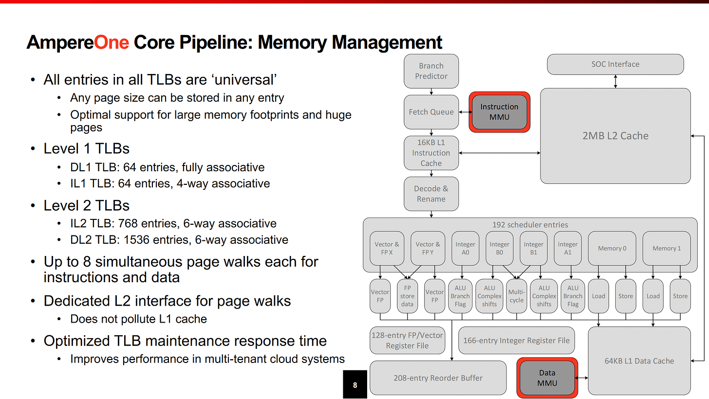
Permissions of course are also enforced through the memory management unit. Ampere emphasizes that their TLBs, which cache virtual to physical address translations, can support any page size with each entry.
Ampere draws a contrast with other architectures that use different TLBs for larger page sizes, often with fewer entries. This can work well for large memory footprint workloads. However, other modern cores like Neoverse V2 and Zen 4 can support 2 MB pages across all TLB sizes. Differences only show up with larger page sizes, which only apply to very specialized applications.
The core supports eight simultaneous page walks for instruction and data. The page walker gets a dedicated interface to L2 to prevent them from polluting the L1 cache during page walks. Ampere also implemented unspecified optimizations for broadcasting TLB maintenance operations, because inefficient broadcast of such operations could be bad at high core counts.
AmpereOne’s private L2 cache is a key part of their strategy for scalability and consistent performance. The L2 can schedule a read and a write every cycle. In testing with a read-modify-write pattern (adding a constant to every element of an array), I was able to sustain 24 bytes per cycle once the test spilled into L2. It’s not quite 32 bytes per cycle, but is better than 16. Ampere also says the L2 can deliver a full 64B line to L1 every cycle, but sustained load bandwidth is limited to 32B/cycle by the load/store unit.
To control power in such a large, low latency cache, Ampere made sure to use the most efficient SRAMs possible for the L2. Control and scheduling logic is centralized instead of being replicated in each data bank. The L2 can track 48 outstanding requests to the rest of the system. There’s also a set of prefetchers at the L2, which feed a prefetch queue that prioritizes the most accurate prefetches. The L2 can throttle its request rate to the system based on feedback from the rest of the SoC.
L2 latency is claimed to be 11 cycles, which aligns with my measurements using a pointer chasing latency microbenchmark. 3.68 nanoseconds is just about 11 cycles at 3 GHz. The large L2 is also critical in my view because it insulates the core from very high system level cache latency.
While not covered in Ampere’s presentation, AmpereOne appears to have similar L3 latency as Nvidia’s Grace CPU. I previously criticized that design for having a small 1 MB L2 cache, as stalls from memory load latency prevented Grace from making the most of its higher clock speed compared to Graviton 4. It’s good to see Ampere use a 2 MB L2 cache. DRAM latency is about 166 ns, much higher than in other server platforms using DDR5. Part of this is likely comes from the cost of traversing the large mesh.
System Level
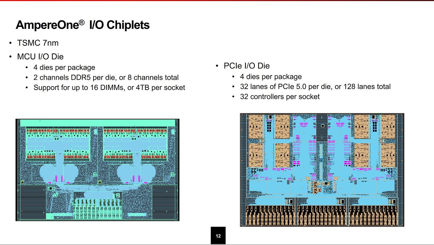
Following an increasingly popular trend, AmpereOne has several chiplets to use the most appropriate process node for different SoC subsystems. AmpereOne is Ampere’s first chiplet setup.
Chiplets are connected to each other using Ampere’s custom die-to-die interconnect. The center compute chiplet, or CCL, is built on TSMC’s 5 nm process. The PCIe and memory controller chiplets are built on TSMC’s 7 nm process. AmpereOne’s chiplet setup allows eight and 12 channel DDR5 setups with the same building blocks. Additionally, the chiplet setup makes it easy to integrate customer IP, should Ampere need to do that.
Within the compute chiplet, cores are arranged in quad core clusters, repeated and arranged in 6 columns of eight clusters each. A subset of quad core clusters are co-located with coherency engines, which contain a slice of system level cache and snoop filters. AmpereOne has enough snoop filter capacity to cover all 384 MB of L2 on the chip.
All of that is arranged on a 8×9 mesh. Ampere states that the mesh is not a completely in-house design, and their official documentation indicates the mesh is based on Arm’s Coherent Mesh Network (CMN). However, Ampere has customized the mesh to support memory tagging and custom cross-die links. From the mesh map in Ampere’s documentation, the 6×8 grid of core clusters are in the bottom center of the mesh. The mesh layout is as follows:
Crosspoints near the corner of the mesh connect to memory controller dies, while the CXRH nodes around the edge serve an unknown function. Ampere wouldn’t tell me, but I suspect they’re die-to-die interfaces that connect to PCIe IO dies. Those also repeat up and down the east/west sides of the die.
The IO dies provide eight DDR5 channels and 128 lanes of PCIe 5.0.
Ampere is proud of being the first company to bring a memory tagging implementation to the datacenter market. Memory tagging can help detect bugs like attempting to use memory that has previously been freed. When memory is allocated, it’s given a tag. Pointers are also tagged with the allocation they’re supposed to access.
With each memory access, the load/store unit compares the pointer’s access tag with the allocation tag. A mismatch will cause the core to raise a fault, indicating that your software has a bug. Beyond helping programmers investigate memory management errors, Ampere says memory tagging can help in cloud environments, and does not incur bandwidth or memory capacity overhead.
At the system level, Ampere uses what they call Adaptive Traffic Management. Ampere already hinted at how this works with the L2 slide. Downstream agents like Coherency Engines (system level cache slices and snoop filters) or memory controllers communicate how busy they are to requesters (cores). Cores then adjust the rate and profile of the traffic they generate.
A core running a latency hungry workload will respond differently to one running a bandwidth hungry workload. As a result, Ampere claims better latency at high bandwidth loads than competitors. Ampere tested this by testing a single latency sensitive application next to increasing numbers of bandwidth hungry applications.
At the rack level, Ampere claims better performance and better performance per watt than AMD’s Genoa and Bergamo.
There is currently no way I can test a physical rack. Oracle cloud won’t even allow access to a whole chip, with a quota of 16 cores likely set for capacity reasons, and getting large comparison systems would be prohibitively costly too. Therefore, I’ll deviate from the presentation from this point on.
Returning to the data from our prior article, AmpereOne provides decent per-core performance. 7-Zip is probably a better case, because it gives the branch predictors on even the most modern cores quite a challenge. Bigger cores likely aren’t able to stretch their reordering capacity muscle as much. AmpereOne here provides comparable clock-for-clock performance as Intel’s Skylake, though Skylake will likely pull ahead at stock clock speeds.
Video encoding with libx264 is a far more difficult task for AmpereOne. Its weak FP/vector side does it no favors, and it falls behind Intel’s density optimized Crestmont cores. Again, the performance gap will only grow if the higher performance cores run at stock clock speeds.
My view is that core for core, AmpereOne doesn’t try to match competing designs from AMD, Intel, or even Arm. Instead, Ampere wants to accommodate more customers in the same physical space. Beyond that, consistent performance takes priority over high performance. Core features like a large private L2 cache align with those goals.
Perhaps the most interesting part of the core is its unconventional cache setup. Besides not going wide and fast, Ampere has gone with a slightly unconventional cache setup. I feel like AmpereOne’s L1 caches are meant to be just good enough to avoid bottlenecking on L2 accesses. It works out though, and AmpereOne remains reasonably well balanced compared to other cores. I didn’t get time to run a lot of workloads on AmpereOne, and Oracle’s cloud doesn’t make it any easier because familiar Linux distributions like Ubuntu and Debian aren’t supported on AmpereOne.
Still, my first impression is that Ampere has made a well balanced core. They make tradeoffs to go after high density, but stopping short of Zen 5 or Redwood Cove performance is a feature. It’s a very good start to the company’s custom CPU design journey, and I look forward to seeing what comes next.


