
AMD's RDNA4 Architecture (Video)

Hello you fine Internet folks,
Today AMD has released their new RDNA4 architecture found in the RX 9000 series, with the RX 9070 and RX 9070 XT GPUs launching first. These are cards targeting the high mid-range of the GPU market but not going after the highest end of the market like they did with RDNA2 and RDNA3.
RDNA4 is the fourth iteration of the RDNA architecture from AMD and it has some very interesting changes and additions compared to prior RDNA architectures.
Acknowledgments
AMD sent over a Powercolor Hellhound RX 9070 and a Powercolor Hellhound RX 9070 XT for review and analysis.
Architectural Improvements
Let’s start with the high-level die diagram changes first.

The die found in the RX 9070 series is fabricated on TSMC’s N4P node and has 53.9 billion transistors on a 356.5mm² die which give a density of roughly 151.2 million transistor per mm².

The majority of the differences between the RX 9070 and the RX 9070 XT are 8 fewer Compute Units, approximately 450MHz boost clock, and an 84-watt power limit reduction.
Cache Bandwidth and Hierarchy Changes
AMD has doubled the number of banks for the L2 cache which has also doubled the amount of L2 per Shader Engine. In prior RDNA architectures there was 1MB of L2 cache per Shader Engine, so the RX 6900 XT had 4MB of L2 cache due to having 4 Shader Engines and the RX 7900 XTX had 6MB of L2 cache due to having 6 Shader Engines.

With RDNA4 AMD has doubled the number of banks per L2 slice which has doubled the bandwidth of each L2 slice as well as doubled the amount of L2 cache per Shader Engine which means with the 4 Shader Engines that the RX 9070 XT has 8MB of L2 cache. It also appears as if AMD also increased the bandwidth of the Infinity Cache (MALL) as well.

What is interesting is that the L1 cache no longer exists on RDNA4. It appears as if the L1 is now a read/write-coalescing buffer and no longer a dedicated cache level. This is a major change in the RDNA cache hierarchy, the L1 was added to RDNA1 in order to reduce the number of requests to the L2 as well as reduce the number of clients to the L2.
Compute Unit and Matrix Unit Updates

AMD added FP operations to the Scalar Unit in RDNA3.5 and they have kept those additions to the Scalar Unit with RDNA4. AMD has also improved the scheduler with Split Barriers which allows instructions to be issued in between completion of consuming or producing one block of work and waiting for other waves to complete their work.
AMD has also added improvements to the register spill and fill behavior in the form of Register Block Spill/Fill operations which operates on up to 32 registers. A major reason for adding this capability was reducing unnecessary spill memory traffic for cases such as separately compiled functions by allowing code that knows which registers contain live state to pass that information to code that may need to save/restore registers to make use of them.
RDNA4 has also significantly beefied-up the matrix units compared to RDNA3. The FP16/BF16 throughput has been doubled along with a quadrupling of the INT8 and INT4 throughput. RDNA4 has also added FP8 (E4M3) along with BF8 (E5M2) at the same throughput as INT8. RDNA4 has also added 4:2 sparsity to its matrix units. However, one part of the Compute Unit that hasn’t seen improvement is the dual-issuing capability.
Ray Accelerator
Moving to the changes to AMD’s Ray Accelerator (RA) which has been a significant focus for AMD with RDNA4.
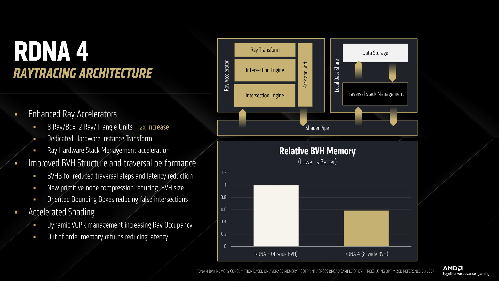
AMD has added a second intersection engine which has doubled the number of ray-box and ray-triangle intersections up from 4 and 1 to 8 and 2 respectively. AMD has also moved from a BVH4 to a BVH8 structure.
AMD has also added the ability for the ray accelerator to store results out of order, “Pack and Sort”. Packing allows the RA to skip ahead and process faster rays that don’t need to access memory or a higher latency cache level. Sorting allows the RA to preserve the correct ordering so that it appears to the program as if the instructions were executed in-order.
Out of Order Memory Access
One of the most exciting things that RDNA4 has added was out of order memory access. This is not like Nvidia’s Shader Execution Reordering, what SER allows for is reordering threads that hit or miss, as well as threads that go to the same cache or memory level, to be bundled in the same wave.

This out of order memory access seems to be very similar to the capabilities that Cortex-A510 has. While the Cortex-A510 is an in-order core for Integer and Floating-Point operations, for memory operations A510 can absorb up to 2 cache misses without stalling the rest of the pipeline. The number of misses that a RDNA4 Compute Unit can handle is unknown but the fact that it can deal with memory accesses out of order is a new feature for a GPU to have.
Dynamic Registers
And last but not least, AMD has added dynamic allocation of RDNA4’s registers.
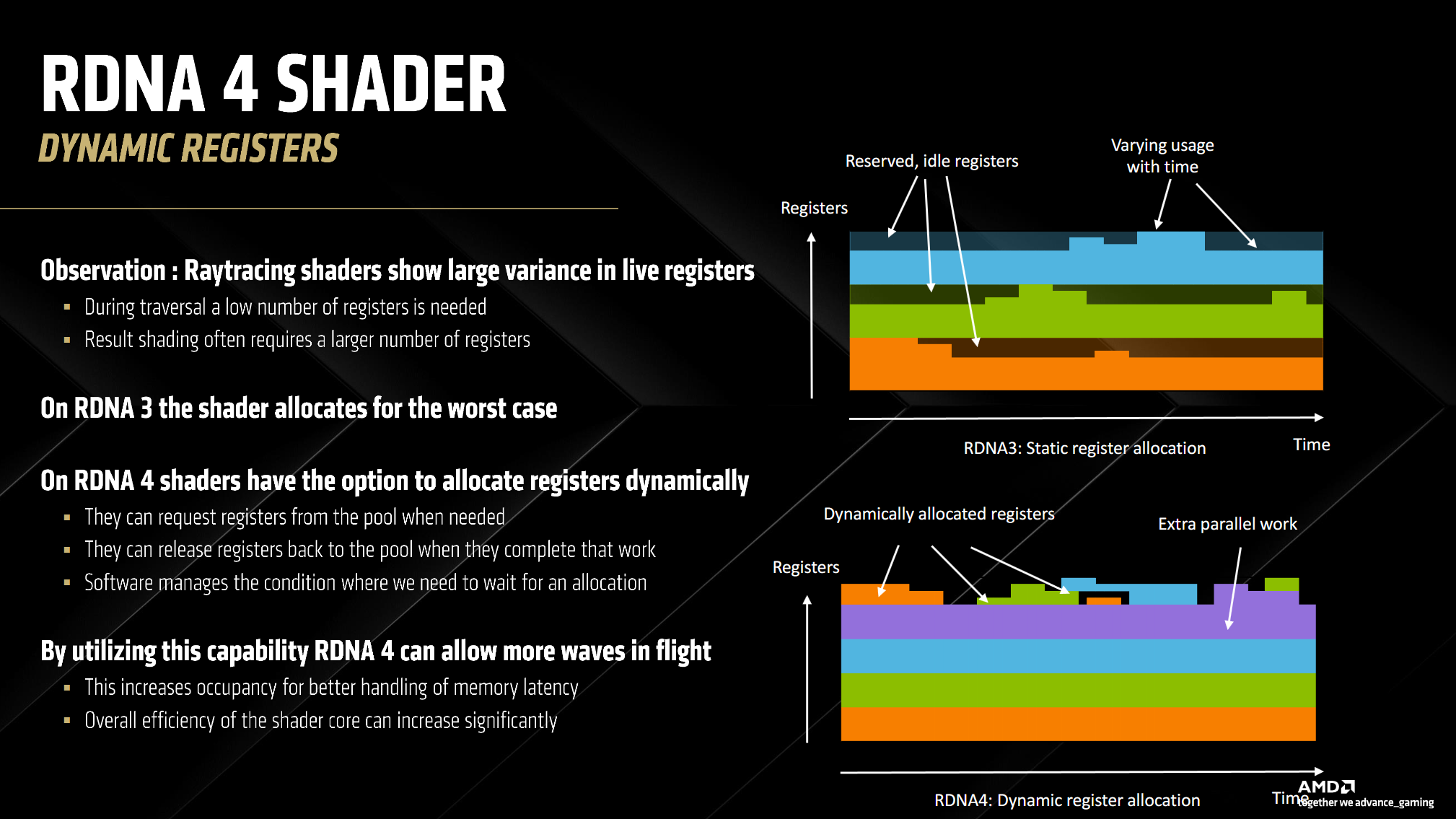
This allows shaders to request more registers than they usually can get. This provides the GPU with more opportunity for having more waves in flight at any given time. Dynamic register allocation along with the out of order memory access gives RDNA4 many tricks to hide the latency that some workloads, in particular ray tracing, have.
Performance of RDNA4 at Different Wattages
I’ll leave the majority of the benchmarking to the rest of the tech media; however, I do want to look at RDNA4’s behavior at various wattages.

The RX 9070 does quite well at 154 watts, despite at being 44% the power compared to the RX 9070 XT at 348W, the RX 9070 at 154 watts get on average 70% the performance of the RX 9070 XT at 348 watts which is a 59% performance per watt advantage for the RX 9070 at 154 watts.
Conclusion
AMD’s brand new RDNA4 architecture has made many improvements to the core of the RDNA compute unit with much improved machine learning and ray tracing accelerators along with major improvements to the handling of latency sensitive workloads.
However, RDNA4’s Compute Unit is not just the only improvements that AMD has made to RDNA4. AMD has also improved the cache bandwidth at the L2 and MALL levels along with making the L1 no longer a cache level but a read/write-coalescing buffer.
However, with the launch of the RX 9070 series, I do wonder what a 500-600mm² RDNA4 die with a 384/512 bit memory bus would have performed like. I wonder if it could have competed with the 4090, or maybe even the 5090.
If you like the content then consider heading over to the Patreon or PayPal if you want to toss a few bucks to Chips and Cheese. Also consider joining the Discord.
I'd love to see a detailed analysis of architectures between RDNA3 vs RDNA4 vs ADA vs Blackwell
Could you analyze this out of order memory more?
If i understand correctly, this is not a traditional cpu like out of order resource, because it doesnt exploit instruction level parallelism, only inter warps memory parallelism.
Do I see it right?