
AMD’s Pre-Zen Interconnect: Testing Trinity’s Northbridge

Today, AMD’s Infinity Fabric interconnect is ubiquitous across the company’s lineup. Infinity Fabric provides well-defined interfaces to a transport layer, and lets different functional blocks treat the interconnect as a black box. The system worked well enough to let AMD create integrated GPU products all the way from the Steam Deck’s tiny van Gogh APU, to giant systems packing four MI300A chips. Across all those offerings, Infinity Fabric enables coherent memory access as CPU and GPU requests converge to Coherent Slaves (CS-es), which have a probe filter and can request data from the appropriate source.
AMD was also trying to build powerful iGPUs over a decade ago, but their interconnect looked very different at the time. Their Northbridge architecture owes its name to the Athlon 64 era, when AMD brought the chipset northbridge’s functionality onto the CPU die. AMD’s engineers likely didn’t envision needing to tightly integrate a GPU during Athlon 64’s development, so the interconnect was designed to tie together a few CPU cores and service memory requests with low latency. But then AMD acquired ATI, and set about trying to take advantage of their new graphics talent by building powerful iGPUs.
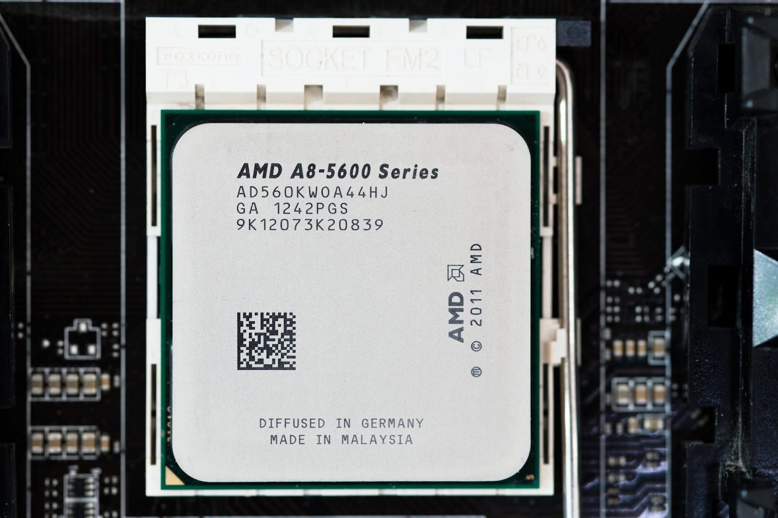
“Trinity” is an AMD Accelerated Processing Unit (APU) from 2012. It combines two dual-threaded Piledriver CPU modules with a 6-SIMD Terascale 3 iGPU. Here I’ll be looking into AMD’s second generation iGPU interconnect with the A8-5600K, a slightly cut-down Trinity implementation with four Terascale 3 SIMDs enabled and CPU boost clocks dropped from 4.2 to 3.9 GHz. I’m testing the chip on a MSI FM2-A75MA-E35 board with 16 GB of Kingston DDR3-1866 10-10-9-26 memory.

Trinity’s on-die network resembles that of AMD’s first APU, Llano, and has clear similarities to AMD’s Athlon 64 Northbridge. The Northbridge sits on a separate voltage and frequency domain, and runs at 1.8 GHz on the A8-5600K. It uses a two-level crossbar setup. CPU cores connect to a System Request Interface (SRI), which routes requests onto a set of queues. Most memory requests head to a System Request Queue (SRQ). The SRI also accepts incoming probes on a separate queue, and routes them to the CPU cores. A second level crossbar, simply called the XBAR, connects with the SRI’s various queues and routes requests to IO and memory. The XBAR can handle IO-to-IO communication too, though such traffic is rare on consumer systems.
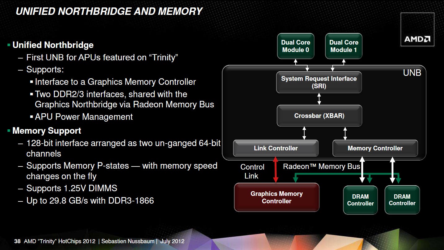
On Trinity, the XBAR’s scheduler (XCS) has 40 entries, making it slightly smaller than the 64 entry XCS on desktop and server Piledriver chips. AMD defaults to a 22+10+8 entry split between the SRI, Memory Controller (MCT),and upstream channel, though the BIOS can opt for a different XCS entry allocation. The XBAR sends memory requests to the MCT, which prioritizes requests based on type and age, and includes a strided-access prefetcher. Like Infinity Fabric’s CS, the MCT is responsible for ensuring cache coherency and can send probes back to the XBAR. The MCT also translates physical addresses to “normalized” addresses that only cover the memory space backed by DRAM.
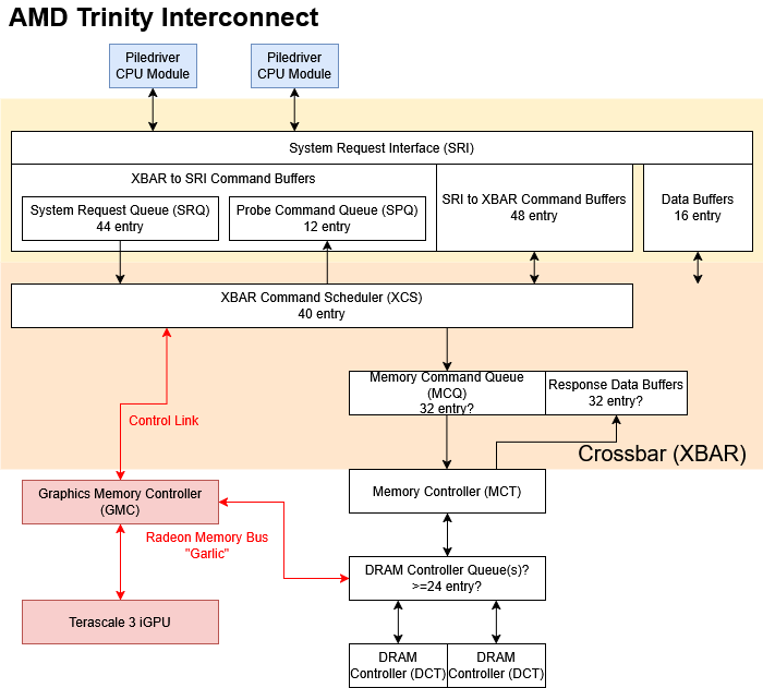
All AMD CPUs from Trinity’s era use a similar SRI+XBAR setup, but Trinity’s iGPU sets it apart from CPU-only products. The iGPU gets its own Graphics Memory Controller (GMC), which arbitrates between different request types and schedules requests to maximize DRAM bandwidth utilization. Thus the GMC performs an analogous role to the MCT on the CPU side. A “Radeon Memory Bus” connects the GMC to the DRAM controllers, bypassing the MCT. AMD documentation occasionally refers to the Radeon Memory Bus as “Garlic”, likely a holdover from internal names used during Llano’s development.
A second control link hooks the GPU into the XBAR, much like any other IO device. Previously, the control link was called the “Fusion Control Link”, or “Onion”. I’ll use “Garlic” and “Onion” to refer to the two links because those names are shorter.
The “Garlic” Link (Radeon Memory Bus)
Trinity’s “Garlic” link lets the GPU saturate DRAM bandwidth. It bypasses the MCT and therefore bypasses the Northbridge’s cache coherency mechanisms. That’s a key design feature, because CPUs and GPUs usually don’t share data. Snooping the CPU caches for GPU memory requests would waste power and flood the interconnect with probes, most of which would miss.
Bypassing the MCT also skips the Northbridge’s regular memory prioritization mechanism, so the MCT and GMC have various mechanisms to keep the CPU and GPU from starving each other of memory bandwidth. First, the MCT and GMC can limit how many outstanding requests they have on the DRAM controller queues (DCQs). Then, the DCQs can alternate between accepting requests from the MCT and GMC, or can be set to prioritize the requester with fewer outstanding requests. Trinity defaults to the former. Finally, because the CPU tends to be more latency sensitive, Trinity can prioritize MCT-side reads ahead of GMC requests. Some of this arbitration seems to happen at queues in front of the DCQ. AMD’s BIOS and Kernel Developer’s Guide (BKDG) indicates there’s a 4-bit read pointer for a sideband signal FIFO between the GMC and DCT, so the “Garlic” link may have a queue with up to 16 entries.

From software testing, Trinity does a good job controlling CPU-side latency under increasing GPU bandwidth demand. Even with the GPU hitting the DRAM controllers with over 24 GB/s of reads and writes, CPU latency remains under 120 ns. Loaded latency can actually get worse under CPU-only bandwidth contention, even though Trinity’s CPU side isn’t capable of fully saturating the memory controller. When testing loaded latency, I have to reserve one thread for running the latency test, so bandwidth in the graph above tops out at just over 17 GB/s. Running bandwidth test threads across all four CPU logical threads would give ~20.1 GB/s.

Mixing CPU and GPU bandwidth load shows that latency goes up when there’s more CPU-side bandwidth. Again, the GPU can pull a lot of bandwidth without impacting CPU memory latency too heavily. Likely, there’s more contention at the SRI and XBAR than at the DRAM controllers.
Control Link, and Cache Coherency (Or Not)
Integrated GPUs raise the prospect of doing zero-copy data sharing between the CPU and GPU, without being constrained by a PCIe bus. Data sharing is conceptually easy, but cache coherency is not, and caching is critical to avoiding DRAM performance bottlenecks. Because requests going through the “Garlic” link can’t snoop caches, “Garlic” can’t guarantee it retrieves the latest data written by the CPU cores.

That’s where the “Onion” link comes in. An OpenCL programmer can tell the runtime to allocate cacheable host memory, then hand it over for the GPU to use without an explicit copy. “Onion” requests pass through the XBAR and get switched to the MCT, which can issue probes to the CPU caches. That lets the GPU access the CPU’s cacheable memory space and retrieve up-to-date data. Unfortunately, “Onion” can’t saturate DRAM bandwidth and tops out at just under 10 GB/s. Trinity’s interconnect also doesn’t come with probe filters, so probe response counts exceed 45 million per second. Curiously, probe response counts are lower than if a probe had been issued for every 64B cacheline.

Northbridge performance counters count “Onion” requests as IO to memory traffic at the XBAR. “Garlic” traffic is not counted at the XBAR, and is only observed at the DRAM controllers. Curiously, the iGPU also creates IO to memory traffic when accessing a very large buffer nominally allocated out of the GPU’s memory space (no ALLOC_HOST_PTR flag), implying it’s using the “Onion” link when it runs out of memory space backed by “Garlic”. If so, iGPU memory accesses over “Onion” incur roughly 320 ns of extra latency over a regular “Garlic” access.

Therefore Trinity’s iGPU takes a significant bandwidth penalty when accessing CPU-side memory, even though both memory spaces are backed by the same physical medium. AMD’s later Infinity Fabric handles this in a more seamless manner, as CS-es observe all CPU and GPU memory accesses. Infinity Fabric CS-es have a probe filter, letting them maintain coherency without creating massive probe traffic.
CPU to iGPU Memory Access
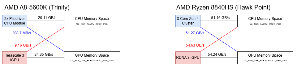
Telling the GPU to access cacheable CPU memory is one way to enable zero-copy behavior. The other way is to map GPU-side memory into a CPU program’s address space. Doing so lets Trinity’s iGPU use its high bandwidth “Garlic” link, and AMD allows this using a CL_MEM_USE_PERSISTENT_MEM_AMD flag. But because the Northbridge has no clue what the GPU is doing through its “Garlic” link, it can’t guarantee cache coherency. AMD solves this by making the address space uncacheable (technically write-combining) from the CPU side, with heavy performance consequences for the CPU.

Besides not being able to enjoy higher bandwidth and lower latency from cache hits, the CPU can’t combine reads from the same cacheline into a single fill request. From the Northbridge perspective, the System Request Interface sends “sized reads” to the XBAR instead of regular “cache block” commands. From Llano’s documentation, the CPU to iGPU memory request path only supports a single pending read, and that seems to apply to Trinity too.

Bandwidth sinks like a stone with the CPU unable to exploit memory level parallelism. Worse, the CPU to iGPU memory path appears less optimized in latency terms. Pointer chasing latency is approximately 93.11 ns across a small 8 KB array. For comparison, requests to cacheable memory space with 2 MB pages achieve lower than 70 ns of latency with a 1 GB array. I’m not sure what page size AMD’s drivers use when mapping iGPU memory into CPU address space, but using a 8 KB array should avoid TLB misses and make the two figures comparable. On AMD’s modern Ryzen 8840HS, which uses Infinity Fabric, there’s no significant latency difference when accessing GPU memory. Furthermore, GPU memory remains cacheable when mapped to the CPU side. However, memory latency in absolute terms is worse on the Ryzen 8840HS at over 100 ns.
Interconnect Traffic in Practice
While AMD had GPU compute in its sights when designing Trinity, its biggest selling point was as a budget gaming solution. Many modern games struggle or won’t launch at all on Trinity, so I’ve selected a few older workloads to get an idea of how much traffic Trinity’s interconnect has to work with.

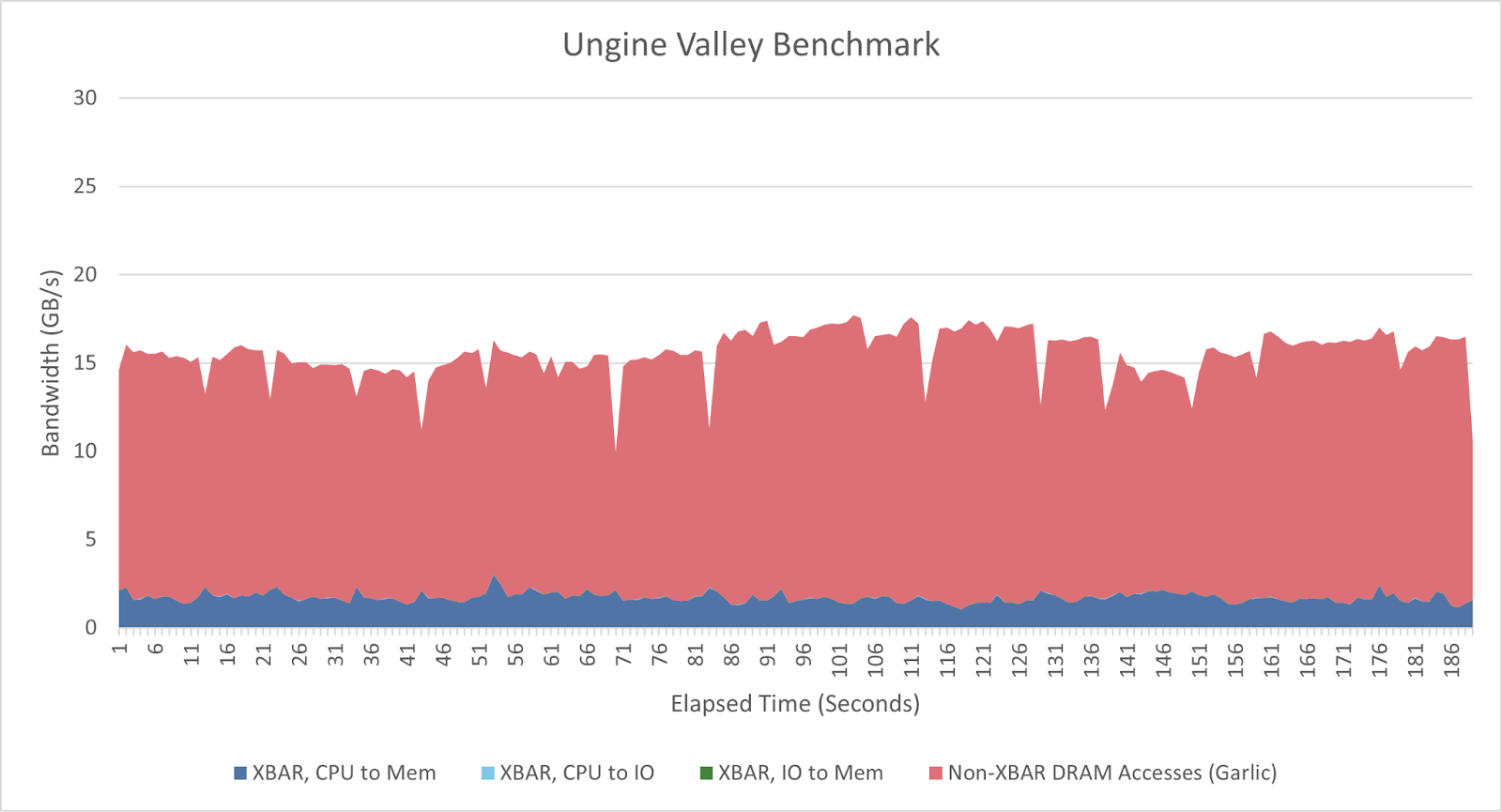
Unigine Valley is a 2013-era DirectX 11 benchmark. Performance counter data collected over a benchmark pass shows plenty of DRAM traffic not observed at the XBAR, which can be attributed to the iGPU’s “Garlic” link. CPU-side memory bandwidth is light, and generally stays below 3 GB/s. Total DRAM traffic peaked at 17.7 GB/s, measured over a 1 second interval.
Final Fantasy 14’s Heavensward benchmark came out a few years after Trinity. With the “Standard (Laptop)” preset running at 1280x720, the A8-5600K averaged 25.6 FPS. Apparently that counts as “Fairly High”, which I only somewhat agree with.

The Heavensward benchmark is more bandwidth hungry, with DRAM bandwidth reaching 22.7 GB/s over a 1 second sampling interval. The CPU side uses more bandwidth too, often staying in the 3-4 GB/s range and sometimes spiking to 5 GB/s. Still, the bulk of DRAM traffic can be attributed to the iGPU, and uses the “Garlic” link.

The Elder Scrolls Online (ESO) is a MMO that launched a few years after Trinity, and can still run on the A8-5600K (if barely) thanks to FSR. I’m running ESO at 1920x1080 with the low quality preset, and FSR set to Quality. Framerate isn’t impressive and often stays below 20 FPS.

CPU bandwidth can often reach into the high 4 GB/s range, though that often occurs when loading in or accessing hub areas with many players around. GPU-side bandwidth demands are lower compared to the two prior benchmarks, and total bandwidth stays under 16 GB/s.
RawTherapee converts camera raw files into standard image formats (i.e. JPEG). Here, I’m processing 45 megapixel raw files from a Nikon D850. RawTherapee only uses the CPU for image processing, so most DRAM traffic is observed through the XBAR, coming from the CPU. The iGPU still uses a bit of bandwidth for display refreshes and perhaps the occasional GPU-accelerated UI feature. In this case, I have the iGPU driving a pair of 1920x1080 60 Hz displays.

Darktable is another raw conversion program. Unlike RawTherapee, Darktable can offload some parts of its image processing pipeline to the GPU. It’s likely the kind of application AMD hoped would become popular and showcase its iGPU prowess. With Darktable, Trinity’s Northbridge handles a mix of traffic from the CPU and iGPU, depending on what the image processing pipeline demands. IO to memory traffic also becomes more than a rounding error, which is notable because that’s how “Onion” traffic is counted. Other IO traffic like SSD reads can also be counted at the XBAR, but that should be insignificant in this workload.

Final Words
In Trinity’s era, powerful iGPUs were an obvious way for AMD to make use of their ATI acquisition and carve out a niche, despite falling behind Intel on the CPU field. However AMD’s interconnect wasn’t ideal for integrating a GPU. The “Onion” and “Garlic” links were a compromise solution that worked around the Northbridge’s limitations. With these links, Trinity doesn’t get the full advantages that an iGPU should intuitively enjoy. Zero-copy behavior is possible, and should work better than doing so with a contemporary discrete GPU setup. But both the CPU and GPU face lower memory performance when accessing the other’s memory space.
Awkwardly for AMD, Intel had a more integrated iGPU setup with Sandy Bridge and Ivy Bridge. Intel’s iGPU sat on a ring bus along with CPU cores and L3 cache. That naturally made it a client of the L3 cache, and unified the CPU and GPU memory access paths at that point. Several years would pass before AMD created their own flexible interconnect where the CPU and GPU could both use a unified, coherent memory path without compromise. Fortunately for AMD, Intel didn’t have a big iGPU to pair with Ivy Bridge.
Trinity’s interconnect may be awkward, but its weaknesses don’t show for graphics workloads. The iGPU can happily gobble up bandwidth over the “Garlic” link, and can do so without destroying CPU-side memory latency. Trinity does tend to generate a lot of DRAM traffic, thanks to a relatively small 512 KB read-only L2 texture cache on the GPU side, and no L3 on the CPU side. Bandwidth hungry workloads like FF14’s Heavensward benchmark can lean heavily on the chip’s DDR3-1866 setup. But even in that workload, there’s a bit of bandwidth to spare. Trinity’s crossbars and separate coherent/non-coherent iGPU links may lack elegance and sophistication compared to modern designs but it was sufficient to let AMD get started with powerful iGPUs in the early 2010s.
If you like the content then consider heading over to the Patreon or PayPal if you want to toss a few bucks to Chips and Cheese. Also consider joining the Discord.
Loved my Llano A6-3400m. Gamed on it.
Thanks Chester, another great dive and (for me) down memory lane with Trinity! One aspect of modern APUs I am curious about is if and how iGPU-assisted compute is actually implemented nowadays. Judging by the now-ubiquitous NPU blocks in designs from both AMD and Intel, the idea of GPU-assisted compute seems to have been abandoned (outside AI), but is it ? Would love to hear your and anyone else's take!