AMD’s Mild Hybrid Strategy: Ryzen Z1 in ASUS’s ROG Ally
Editor’s Note: ASUS sent us the ROG Ally sample – our first review sample from a company – in order to test the Ryzen Z1 SOC inside the device. So a massive thank you to them!
CPUs with hybrid core configurations have become mainstream as chip makers look to get the best of all worlds. ARM started to use big.LITTLE configurations for mobile SoCs a decade ago. Intel’s Lakefield chip combined one Sunny Cove performance core with four Tremont efficiency cores. AMD has resisted this trend – and for good reason, as hybrid configurations are more difficult to optimize for software. But things have been changing with Zen 4. The Ryzen 9 7950X3D uses cores with two different L3 cache configurations in an attempt to optimize performance for applications that either prefer high clock speeds or more cache.
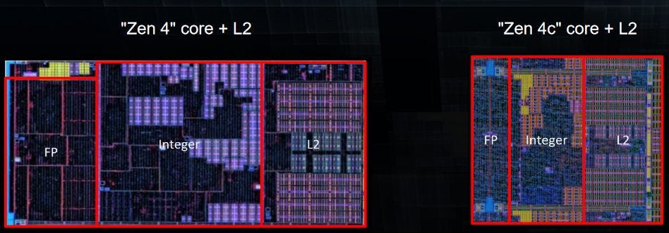
AMD’s Ryzen Z1 is another semi-hybrid core configuration. Instead of different L3 cache configurations, the Ryzen Z1 combines two high-performance Zen 4 cores with four density-optimized Zen 4c cores. Zen 4c cores are architecturally identical to regular Zen 4 cores, but sacrifice high clock speeds for smaller die areas. Today, we’ll be looking at the Ryzen Z1 as implemented by ASUS in the ROG Ally.
Clock Behavior
The Ryzen Z1’s Zen 4 cores can clock up to 5 GHz, while the Zen 4c cores stop at 3.55 GHz. ASUS has configured the ROG Ally to ramp clocks very quickly, and both cores reach their maximum clock speed in just over 1.5 ms.
Cache and Memory Latency
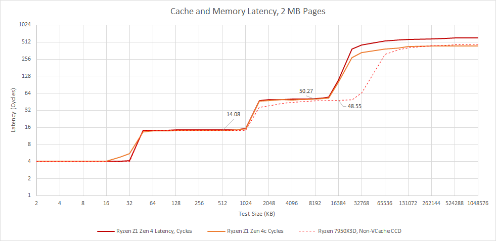
AMD claims Zen 4 and Zen 4c cores are architecturally identical, and thus we see identical L1 and L2 latencies in terms of cycles. L1 has 4 cycles of load-to-use latency, and L2 has 14.
L3 latency is just above 50 cycles on the Ryzen Z1 from both Zen 4 and Zen 4c cores. Desktop Zen 4 can access its L3 in 1-2 fewer cycles, even though it has a larger 32 MB L3. The Ryzen Z1 only has 16 MB of L3 cache.
True latency is higher on Zen 4c due to lower clocks. L3 latency is mediocre at 14.16 ns, while regular Zen 4 cores enjoy 10.46 ns of L3 latency. Desktop Zen 4 cores clock even higher because they aren’t restricted by the tight power and thermal limitations imposed by a mobile platform.
The Ryzen Z1 is equipped with LPDDR5 memory, which shows much higher latency than desktop DDR5 memory. Z1’s situation is therefore similar to Van Gogh. Both chips take a double whammy of a smaller L3 cache and higher latency access to main memory. However, the Z1 is better off in absolute terms. Its 123.9 ns of main memory latency is better than Van Gogh’s 155 ns. A 16 MB L3 cache is also worlds better than a 4 MB one.
L3 Latency with Multiple Cores Active
The L3 cache on AMD’s Zen lineup is tightly coupled to the CPU cores and runs at the speed of the fastest core. It’s a massive improvement over Bulldozer, whose poorly performed L3 was placed behind the on-die northbridge. The L3 improvement allowed Zen to architecturally compete with Intel, who enjoyed a considerable L3 performance advantage up to that point. Unlike Intel, whose L3 clocks was decoupled from the cores since Haswell, AMD kept the L3 clock tied to core clock. Different cores can still run at different clocks thanks to per-core dividers. But those dividers aren’t infinitely flexible. They can only be adjusted in 1/8 divide steps, and core frequency can’t be too far from L3 frequency.
L3/L2 fifo logic related to 4-cycle data heads-up requires core to be 1/3 of L3 frequency or higher[…] core and L3 frequencies below 400MHz are not supported by the architecture.
Zen 4 Processor Programming Reference
Those limitations weren’t an issue for Ryzen CPUs up to now, because the delta between the fastest and slowest core in a cluster is quite small. Ryzen Z1 is more interesting because cores in the same cluster can simultaneously run at 5 GHz and 3.55 GHz. While a significant difference, Zen’s L3 design has no issues having one core run at ~3/4 the frequency of the fastest one.
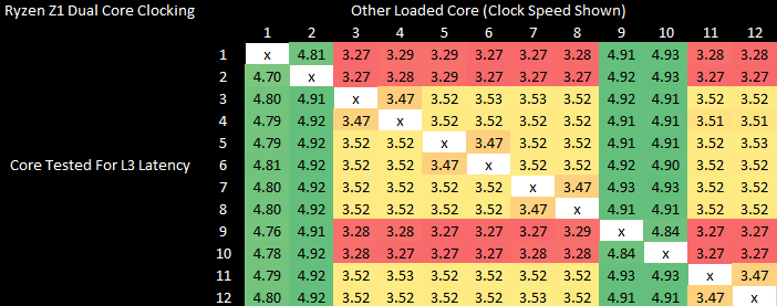
The table above shows measured L3 latency in nanoseconds from each core with a dummy load on another core. Logical cores 1,2 and 9,10 are hardware threads on Zen 4 cores, while the rest are Zen 4c. Zen 4 cores don’t take a L3 latency penalty if a Zen 4c core is active. For Zen 4c cores, having a Zen 4 core active slightly improves L3 latency. Likely, the L3 continues to run at the speed of the fastest core.
Since I had to put a dummy load on a second thread, I took the opportunity to make it a clock speed test. Like the boost clock test at the start of this article, I’m inferring clock speed from register-to-register integer addition latency. The dummy thread reports how many adds it was able to complete while watching a specific memory location that the test thread uses to indicate it’s done.
Ryzen Z1’s Zen 4 cores always run at maximum clock regardless of which other core is active. The Zen 4c cores reach their maximum 3.55 GHz clock if the other active core is also a Zen 4c core. If a vanilla Zen 4 core is active though, the Zen 4c core runs at 3.3 GHz.
In comparison, the differences in the L3 latency on AMD’s desktop Ryzen 7950X3D is negligible as different pairs of cores are loaded. The 7950X3D’s V-Cache enabled die does see lower clock speeds, but the two dies act as separate clusters with different L3 cache instances. Thus the chip’s largest clock speed delta doesn’t come into play as cores on the two dies can clock independently.
Within each die, the 7950X3D acts like a homogeneous setup. There are minor variations in frequency between cores, but nothing like what the Ryzen Z1 exhibits:
Cache and Memory Bandwidth
Bandwidth is in a similar situation. Zen 4c has similar per-cycle read bandwidth to regular Zen 4. It can pull just under 64 bytes per cycle from L1, 32 bytes per cycle from L2, and 26-27 bytes per cycle from L3.
From DRAM, a single Zen 4c core can pull just over 41 GB/s. Regular Zen 4 cores enjoy a bit more DRAM bandwidth, but I suspect the difference is again affected by clock speed.
Multithreaded Memory Read Bandwidth
The higher clocked Zen 4 cores may be individually ahead, but the Ryzen Z1 has twice as many Zen 4c cores. Together, the four Zen 4c cores enjoy more cache bandwidth than the two Zen 4 cores.
Once we get out of caches, memory bandwidth is around 49 GB/s regardless of whether the test uses two Zen 4 cores or four Zen 4c cores. Both are more than capable of saturating the memory controller.
Hybrid setups are prone to long tailed behavior where threads that end up on big cores finish faster, leaving the chip under-utilized as the workload finishes. That makes memory bandwidth testing difficult. To get around this, I’m using a heavily modified version of my memory bandwidth benchmark. Threads are each pinned to a core. Iterations (work) per thread are adjusted until the runtime of the fastest and slowest threads are no more than 10% apart.

With the modified test, Ryzen Z1 shows a peak of 1.329 TB/s of L1 data cache bandwidth, and later drops to just over 1.27 TB/s as the chip starts to thermal throttle. If we estimate clock speeds by dividing measured bandwidth by Zen 4’s theoretical 64 bytes per cycle of load bandwidth, the vanilla Zen 4 cores were running somewhere north of 4.3 GHz toward the end of the L1-sized test region, and the Zen 4c cores ran at about 2.9 GHz.
L2 and L3 bandwidth end up at ~700 GB/s and 540 GB/s respectively. Those figures are a good showing for a six-core setup, especially one in a handheld device. However, when comparing to six Zen 4 cores in a desktop configuration, it’s clear that compromises are necessary in a mobile device. Better cooling and higher power targets allow higher clock speeds, and desktop Zen 4 pulls ahead by a massive 44.8% in L1 bandwidth. Margins are similar when hitting L2 and L3 caches. When the test spills out to main memory, the gap closes as clock speed differences stop mattering in the face of a memory bandwidth bottleneck. The six Zen 4 cores from the Ryzen 7950X3D enjoy just a 6.6% DRAM bandwidth advantage over the Ryzen Z1.
Core to Core Latency
CPUs have to provide a coherent view of memory across multiple cores even when each core has private caches. If one core writes to its private cache and another core needs to see the write, the CPU will have to snoop the first core’s caches to ensure the reading core gets an up-to-date view of memory. I’m testing latency for this sequence with atomic compare and swap operations.
Even though the Ryzen Z1 has two different CPU core types, performance with atomics is unaffected. All cores are part of the same L3 cluster, so coherency is handled by the L3 slice the tested address is homed to.
AMD’s design contrasts with that of Intel’s hybrid architectures. Meteor Lake and Alder Lake’s E-Cores have a separate level of shared caches. Meteor Lake introduces another E-Core type that doesn’t sit on the L3, so coherency has to be handled at multiple levels. Thus Intel shows higher variation in latency for atomics than AMD’s design.
Vector Compute Throughput
I’ve seen presentations throw around massive throughput numbers for GPUs and other accelerators, but CPUs have vector units too, and particularly x86 CPUs tend to have excellent vector performance. For fun, I wrote a vector throughput test that uses the same mitigation strategy for hybrid architectures as the modified memory bandwidth test above. Iteration counts are adjusted until the slowest and fastest threads are within 10%, except 20% on Qualcomm due to noisy mobile OS environments.
Despite sitting in the low power segment, the Ryzen Z1 is capable of over 1 TFLOPS of FP32 performance. That gives it substantially higher vector throughput than the Maxwell iGPU in Nintendo’s Switch. On the integer side, Zen 4 and Zen 4c both have four vector math pipes capable of handling packed integer additions with impressive performance.

Desktop Zen 4 benefits from higher power targets and thus higher clock speeds. Six Zen 4 cores on the Ryzen 7950X3D easily outpace Ryzen Z1. Qualcomm’s Snapdragon 8+ Gen 1 is another interesting comparison. Qualcomm’s chip uses one Cortex X2, three Cortex A710, and four Cortex A510 cores. Pairs of A510 cores share a vector unit, and A710 has mediocre vector throughput. On top of that, the Snapdragon 8+ Gen 1 has to make do with passive cooling in a cell phone. Ryzen Z1’s vector throughput is on a different planet.
But that’s not necessarily a good thing. A low power CPU like the Ryzen Z1 is probably not expected to handle vector-heavy workloads like video encoding, photo editing, or n-body simulations. Snapdragon 8+ Gen 1 may be a better fit for web browsing and email checking. Games also tend to have modest demands for vector performance.
Final Words
CPU designers face a litany of competing demands. An ideal core has high density, high performance, and low power consumption, but these demands are often at odds with each other. For example, circuitry capable of higher clocks at lower power often consumes more die area. CPU core design is always a compromise, with designers looking to strike the best balance with competing demands in mind. ARM and Intel have adopted heterogeneous setups, finding it difficult to meet the ever-increasing conflicting demands by further compromising on one homogeneous design.
AMD stuck with a more homogeneous setup, and for good reasons. Similar cores are easier for software to target without performance loss due to long-tailed behavior. Different core designs also require more engineering resources. Despite its recent growth, AMD is still a much smaller company than Intel, and cannot afford to use its engineering resources inefficiently.

Therefore, AMD’s hybrid strategy is more conservative than Intel’s or ARM’s. Instead of using different core designs, AMD redid Zen 4’s physical design to shrink the core at the expense of frequency. By doing so, AMD’s work on the Zen 4 architecture serves both Zen 4 and Zen 4c cores. Zen 4c still requires additional engineering resources to create and validate its different physical design, but the investment should be significantly less than what’s required for a ground-up redesign.
On one hand, using the same architecture for Zen 4 and Zen 4c limits AMD’s optimization potential. Intel could use a 3-cycle L1d in Gracemont, taking advantage of low clocks to reduce pipeline depth. Zen 4 and Zen 4c both have 4-cycle L1d caches, even though a 3-cycle L1d should be possible at Zen 4c’s low clock targets. On the other hand, keeping the same core design avoids Intel’s troubles with mismatched ISA extension support. AVX-512 is supported across all of Ryzen Z1’s cores, while Intel has disabled AVX-512 on their hybrid designs. General optimization is also easier for AMD’s Ryzen Z1, because any architecture-specific optimization done for Zen 4 are still applicable to Zen 4c.
Zooming out, Zen 4 feels like the start of a conservative hybrid strategy from AMD. On the desktop scene, AMD’s Ryzen 7950X3D mixes cache configurations and has mild clock speed differences. For portable devices, the Ryzen Z1 here mixes cores with different physical designs and has larger clock speed deltas across the chip. AMD’s other consumer offerings do not use hybrid configurations. It’s a clear contrast from Intel’s strategy since Alder Lake, where hybrid setups are used across a large portion of Intel’s consumer CPU lineup.
AMD’s hybrid strategy makes a lot of sense today as the vastly smaller company contends with both Intel and NVIDIA. But there was a time when AMD maintained two concurrent core architecture lineups. In the early 2010s, Bobcat and Jaguar covered low-power applications while Bulldozer went for high performance. It’ll be interesting to see whether AMD treads back in that direction, or Zen 4’s conservative hybrid strategy is here to stay.
We would like to thank ASUS again for providing a review sample that makes this article possible.
If you like our articles and journalism, and you want to support us in our endeavors, then consider heading over to our Patreon or our PayPal if you want to toss a few bucks our way. If you would like to talk with the Chips and Cheese staff and the people behind the scenes, then consider joining our Discord.


