
AMD’s Magny Cours and HyperTransport Interconnect: A High Core Count Blast from the Past

Today, we’re used to desktop processors with 16 or more cores, and several times that in server CPUs. But even prior to 2010, Intel and AMD were working hard to reach higher core counts. AMD’s “Magny Cours”, or Opteron 6000 series, was one such effort. Looking into how AMD approached core count scaling with pre-2010s technology should make for a fun retrospective. Special thanks goes to cha0shacker for providing access to a dual socket Opteron 6180 SE system.
A Magny Cours chip is basically two Phenom II X6 CPU dies side by side. Reusing the prior generation’s 6-core die reduces validation requirements and improves yields compared to taping out a new higher core count die. The two dies are connected via HyperTransport (HT) links, which previously bridged multiple sockets starting from the K8 generation. Magny Cours takes the same concept but runs HyperTransport signals through on-package PCB traces. Much like a dual socket setup, the two dies on a Magny Cours chip each have their own memory controller, and cores on a die enjoy faster access to locally attached memory. That creates a NUMA (Non-Uniform Memory Access) setup, though Magny Cours can also be configured to interleave memory accesses across nodes to scale performance with non-NUMA aware code.

Magny Cours’s in-package links have an awkward setup. Each die has four HT ports, each 16 bits wide and capable of operating in an “unganged” mode to provide two 8-bit sub links. The two dies are connected via a 16-bit “ganged” link along with a 8-bit sublink from another port. AMD never supported using the 8-bit cross-die link though, perhaps because its additional bandwidth would be difficult to utilize and interleaving traffic across uneven links sounds complicated. Magny Cours uses Gen 3 HT links that run at up to 6.4 GT/s, so the two dies have 12.8 GB/s of bandwidth between them. Including the disabled 8-bit sublink would increase intra-package bandwidth to 19.2 GB/s.

With one and a half ports connected within a package, each die has 2.5 HT ports available for external connectivity. AMD decided to use those to give a G34 package four external HT ports. One is typically used for IO in single or dual socket systems, while the other three connect to the other socket.

Quad socket systems get far more complicated, and implementations can allocate links to prioritize either IO bandwidth or cross-socket bandwidth. AMD’s slides show a basic example where four 16-bit HT links are allocated to IO, but it’s also possible to have only two sockets connect to IO.
HyperTransport Performance
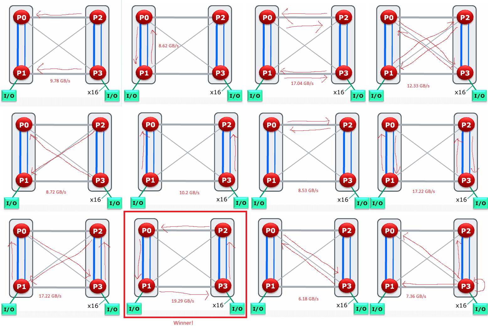
In the dual socket setup we’re testing with here, two ports operate in “ganged” mode and connect corresponding dies on the two sockets. The third port is “unganged” to provide a pair of 8-bit links, which connect die 0 on the first socket to die 1 on the second socket, and vice versa. That creates a fully connected mesh. The resulting topology resembles a square, with more link bandwidth along its sides and less across its diagonals.
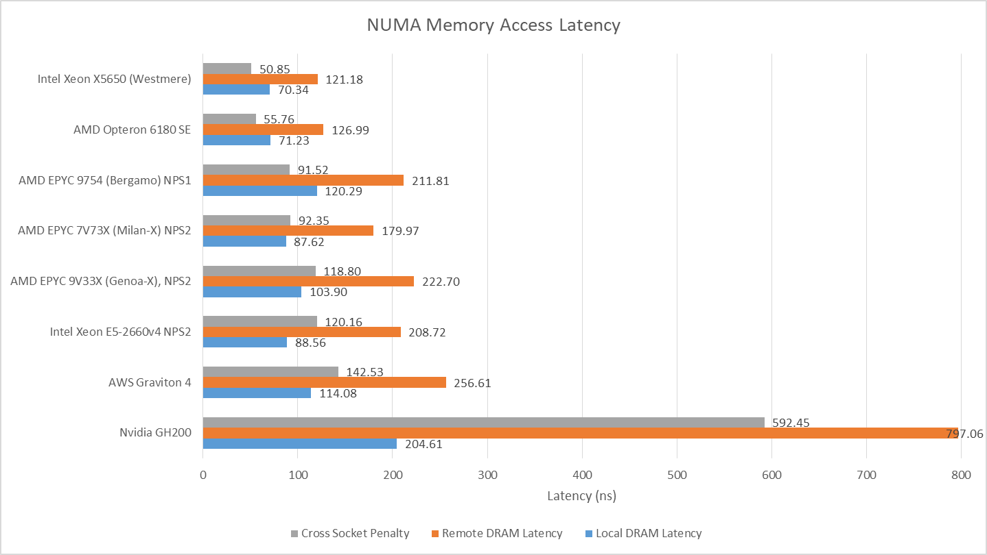
Cross-node memory latency is 120-130 ns, or approximately 50-60 ns more than a local memory access. Magny Cours lands in the same latency ballpark as a newer Intel Westmere dual socket setup. Both dual socket systems from around 2010 offer significantly lower latencies for both local and remote accesses compared to modern systems. The penalty for a remote memory access over a local one is also lower, suggesting both the memory controllers and cross-socket links have lower latency.
Core to Core Latency
Like prior AMD generations, Magny Cours’s memory controllers (MCTs) are responsible for ensuring coherency. They can operate in a broadcast mode, where the MCTs probe everyone with each memory request. While simple, this scheme creates a lot of probe traffic and increases DRAM latency because the MCTs have to wait for probe responses before returning data from DRAM. Most memory requests don’t need data from another cache, so AMD implemented an “HT assist” option that reserves 1 MB of L3 cache per die for use as a probe filter. The MCTs use the probe filter to remember which lines in its local address space are cached across the system and if so, what state they’re cached in.

Regardless of whether HT assist is enabled, Magny Cours’s MCTs are solely responsible for ensuring cache coherency. Therefore, core to core transfers must be orchestrated by the MCT that owns the cache line in question. Cores on the same die may have to exchange data through another die, if the cache line is homed to that other die. Transfers within the same die have about 180 ns of latency, with a latency increase of an extra ~50 ns to the other die within the same socket. In the worst case, latency can pass 300 ns when bouncing a cache line across three dies (two cores on separate dies, orchestrated by a memory controller on a third die).

For comparison, Intel’s slightly newer Westmere uses core valid bits at the L3 cache to act as a probe filter, and can complete core to core transfers within the same die even if the address is homed to another die. Core to core latencies are also lower across the board.
Bandwidth
The bandwidth situation with AMD’s setup is quite complicated because it’s a quad-node system, as opposed to the dual-node Westmere setup with half as many cores. Magny Cours connected via 16-bit HT links gets about 5 GB/s of bandwidth between them, with slightly better performance over an intra-package link as opposed to a cross-socket one. Cross-node bandwidth is lowest over the 8-bit “diagonal” cross-socket links, at about 4.4 GB/s.

From a simple perspective of how fast one socket can read data from another, the Opteron 6180 SE lands in the same ballpark as a Xeon X5650 (Westmere) system. Modern setups of course enjoy massively higher bandwidth, thanks to newer DDR versions, wider memory buses, and improved cross-socket links.

Having cores on both sockets read from the other’s memory pool brings cross-socket bandwidth to just over 17 GB/s, though getting that figure requires making sure the 16-bit links are used rather than the 8-bit ones. Repeating the same experiment but going over the 8-bit diagonal links only achieves 12.33 GB/s. I was able to push total cross-node bandwidth to 19.3 GB/s with a convoluted test where cores on each die read from memory attached to another die over a 16-bit link. To summarize, refer to the following simple picture:
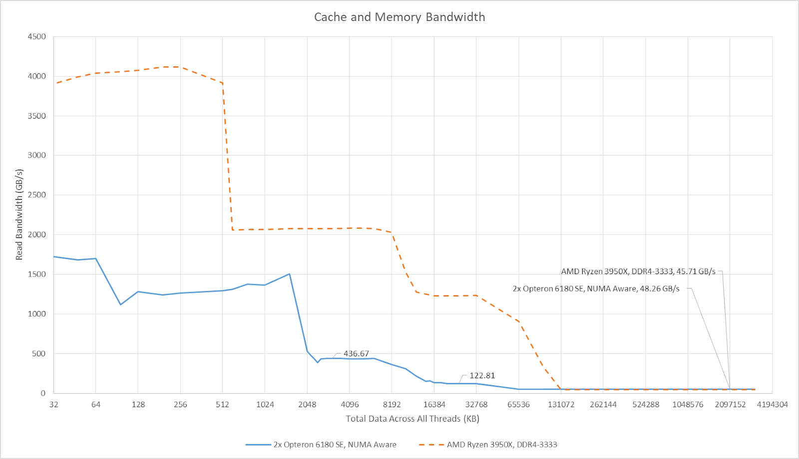
NUMA-aware applications will of course try to keep memory accesses local, and minimize the more expensive accesses over HyperTransport links. I was able to achieve just over 48 GB/s of DRAM bandwidth across the system with all cores reading from their directly attached memory pools. That gives the old Opteron system similar DRAM bandwidth to a relatively modern Ryzen 3950X setup. Of course, the newer 16-core chip has massively higher cache bandwidth and doesn’t have NUMA characteristics.
Intra-Die Interconnect
Magny Cours’s on-die network, or Northbridge, bridges its six cores to the local memory controller and HyperTransport links. AMD’s Northbridge design internally consists of two crossbars, dubbed the System Request Interface (SRI) and XBAR. Cores connect to the SRI, while the XBAR connects the SRI with the memory controller and HyperTransport links. The two-level split likely reduces port count on each crossbar. 10h CPUs have a 32 entry System Request Queue between the SRI and XBAR, up from 24 entries in earlier K8-based Opterons. At the XBAR, AMD has a 56 entry XBAR Scheduler (XCS) that tracks commands from the SRI, memory controller, and HyperTransport links.
Crossbar: This topology is simple to build, and naturally provides an ordered network with low latency. It is suitable where the wire counts are still relatively small. This topology is suitable for an interconnect with a small number of nodes
Arm’s AMBA 5 CHI Architecture Specification (https://kolegite.com/EE_library/datasheets_and_manuals/FPGA/AMBA/IHI0050E_a_amba_5_chi_architecture_spec.pdf), on the tradeoffs between crossbar, ring, and mesh interconnects
The crossbar setup in AMD’s early on-die network does an excellent job of delivering low memory latency. Baseline memory latency with just a pointer chasing pattern is 72.2 ns. Modern server chips with more complicated interconnects often see memory latency exceed 100 ns.
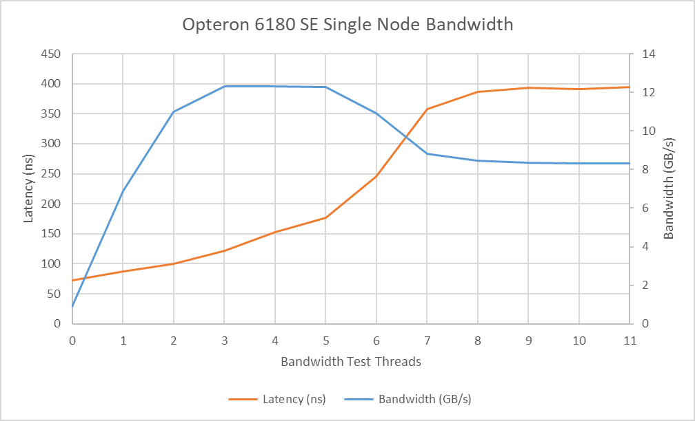
As bandwidth demands increase, the interconnect does a mediocre job of ensuring a latency sensitive thread doesn’t get starved by bandwidth hungry ones. Latency increases to 177 ns with the five other cores on the same die generating bandwidth load, which is more than a 2x increase over unloaded latency. Other nodes connected via HyperTransport can generate even more contention on the local memory controller. With cores on another die reading from the same memory controller, bandwidth drops to 8.3 GB/s, while latency from a local core skyrockets to nearly 400 ns. Magny Cours likely suffers contention at multiple points in the interconnect. The most notable issue though is poor memory bandwidth compared to what the setup should be able to achieve.

Three cores are enough to reach bandwidth limits on Magny Cours, which is approximately 10.4 GB/s. With dual channel DDR3-1333 on each node, the test system should have 21.3 GB/s of DRAM bandwidth per node, or 85.3 GB/s across all four nodes. However, bandwidth testing falls well short: even when using all 6 cores to read from a large array, a single die on the Opteron 6180 SE is barely better than a Phenom II X4 945 with DDR2-800, and slightly worse than a Phenom X4 9950 with fast DDR2. This could be down to the low 1.8 GHz northbridge clock and a narrow link to the memory controller (perhaps 64-bit), or insufficient queue entries at the memory controller to absorb DDR latency. Whatever the case, Magny Cours leaves much of DDR3’s potential bandwidth advantage on the table. This issue seems to be solved in Bulldozer, which can achieve well over 20 GB/s with a 2.2 GHz northbridge clock.
Single Thread Performance: SPEC CPU2017
Magny Cours is designed to deliver high core count, not maximize single threaded performance. The Opteron 6180 SE runs its cores at 2.5 GHz and northbridge at 1.8 GHz, which is slower than even first-generation Phenoms. With two desktop dies in the same package, AMD needs to use lower clock speeds to keep power under control. Single-threaded SPEC CPU2017 scores are therefore underwhelming. The Opteron 6180 SE comes in just behind Intel’s later Goldmont Plus core, which can clock up to 2.7 GHz.

AMD’s client designs from a few years later achieved much better SPEC CPU2017 scores. The older Phenom X4 9950 takes a tiny lead across both test suites. Its smaller 2 MB L3 cache is balanced out by higher clocks, with an overclock to 2.8 GHz really helping it out. Despite losing 1 MB of L3 for use as a probe filter and thus only having 5 MB of L3, the Opteron 6180 maintains a healthy L3 hit rate advantage over its predecessor.

The exact advantage of the larger L3 can vary of course. 510.parset is a great showcase of what a bigger cache can achieve, with the huge hit rate difference giving the Opteron 6180 SE a 9.4% lead over the Phenom X4 9950. Conversely, 548.exchange2 is a high IPC test with a very tiny data footprint. In that subtest, the Phenom X4 9950 uses its 12% clock speed advantage to gain a 11% lead.
Final Words
Technologies available in the late 2000s made core count scaling a difficult task. Magny Cours employed a long list of techniques to push core counts higher while keeping cost under control. Carving a snoop filter out of L3 capacity helps reduce die area requirements. At a higher level, AMD reuses a smaller die across different market segments, and uses multiple instances of the same die to scale core counts. As a result, AMD can keep fewer, smaller dies in production. In some ways, AMD’s strategy back then has parallels to their current one, which also seeks to reuse a smaller die across different purposes.
While low cost, AMD’s approach has downsides. Because each hexacore die is a self-contained unit with its own cores and memory controller, Magny Cours relies on NUMA-aware software for optimal performance. Intel also has to deal with NUMA characteristics when scaling up core counts, but their octa-core Nehalem-EX and 10-core Westmere EX provide more cores and more memory bandwidth in each NUMA node. AMD’s HyperTransport and low latency northbridge do get credit for keeping NUMA cross-node costs low, as cross-node memory accesses have far lower latency than in modern designs. But AMD still relies more heavily on software written with NUMA in mind than Intel.
Digging deeper reveals quirks with Magny Cours. Memory bandwidth is underwhelming for a DDR3 system, and the Northbridge struggles to maintain fairness under high bandwidth load. A four-node system might be fully connected, but “diagonal” links have lower bandwidth. All of that makes the system potentially more difficult to tune for, especially compared to a modern 24-core chip with uniform memory access. Creating a high core count system was quite a challenge in the years leading up to 2010, and quirks are expected.
But Magny Cours evidently worked well enough to chart AMD’s scalability course for the next few generations. AMD would continue to reuse a small die across server and client products, and scaled core count by scaling die count. Even for their Bulldozer Opterons, AMD kept using this general setup of four sockets with 2 dies each, only updating it for Zen1, which is perhaps the ultimate evolution of the Magny Cours strategy, hitting four dies per socket and replacing the Northbridge/HyperTransport combination with Infinity Fabric components. Today, AMD continues to use a multi-die strategy, though with more die types (IO dies and CCDs) to provide more uniform memory access.
If you like the content then consider heading over to the Patreon or PayPal if you want to toss a few bucks to Chips and Cheese. Also consider joining the Discord.
Wow, this is indeed a blast from the past! Fun fact: I have some rare AMD Magny-Cours ES samples lying around. I remember, back in the day, we considered Magny-Cours not for SMP applications, but for workloads that relied on single-core performance—essentially large, VM-based applications. As Chester pointed out, Intel's approach was better at the time, but AMD played the long game, sticking with the same technique for a long time. They constantly made refinements that ultimately led to the groundbreaking Zen1 architecture. Fun times indeed.