
Alibaba/T-HEAD's Xuantie C910

T-HEAD is a wholly owned subsidiary of Alibaba, one of China's largest tech companies. Over the past few years, T-HEAD has created a line of RISC-V cores. Alibaba seems to have two motivations for pushing RISC-V. On one hand, the company stands to benefit from creating cost effective chips optimized for areas it cares about, like IoT endpoints and edge computing. On the other, Alibaba almost certainly wants to reduce its dependence on foreign imports. RISC-V is an open instruction set, and isn't controlled by US or British corporations like x86-64 or ARM. T-HEAD's RISC-V push can thus be seen more broadly as a part of China's push to create viable domestic microchips.

Xuantie C910 slots into the "high performance" category within T-HEAD's lineup. Besides joining a small number of out-of-order RISC-V cores that have made it into hardware, C910 is an early adopter for RISC-V's vector extension. It supports RVV 0.7.1, which features masking and variable vector length support. T-HEAD has since released the C920 core, which brings RVV support up to version 1.0, but otherwise leaves C910 unchanged.

C910 targets "AI, Edge servers, Industrial control, [and] ADAS" as possible applications. It's also T-HEAD's first generation out-of-order design, so taking on all those applications is ambitious. C910 is implemented in clusters of up to four cores, each with a shared L2 cache. T-HEAD targets 2 to 2.5 GHz on TSMC's 12nm FinFET process, where a C910 core occupies 0.8 mm2. Core voltage is 0.8V at 2 GHz, and 1.0V at 2.5 GHz. On TSMC's 7nm process, T-HEAD managed to push core frequency to 2.8 GHz. T-HEAD's paper further claims dynamic power is around 100 microwatts/MHz, which works out to 0.2W at 2 GHz. Of course, this figure doesn't include static power or power draw outside the core. Yet all of these characteristics together make clear C910 is a low power, low area design.

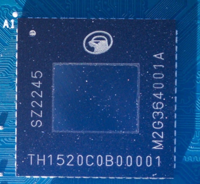
This article will examine C910 in the T-HEAD TH1520, using the LicheePi single board computer. TH1520 is fabricated on TSMC’s 12nm FinFET process, and has a quad-core C910 cluster with 1 MB of L2 running at 1.85 GHz. It’s connected to 8 GB of LPDDR4X-3733. C910 has been open-sourced, so I’ll be attempting to dig deeper into core details by reading some of the source code – but with some disclaimers. I’m a software engineer, not a hardware engineer. Also, some of the code is likely auto-generated from another undisclosed source, so reading that code has been a time consuming and painful experience. Expect some mistakes along the way.
Core Overview
The Xuantie C910 is a 3-wide, out-of-order core with a 12 stage pipeline.

Like Arm’s Cortex A73, C910 can release out-of-order resources early. For microbenchmarking, I used both a dependent branch and incomplete load to block retire, just as I did on A73.

Frontend: Instruction Fetch and Branch Prediction
C910’s frontend is tailored to handle both 16-bit and 32-bit RISC-V instructions, along with the requirements of RISC-V’s vector extension. The core has a 64 KB, 2-way set associative instruction cache with a FIFO replacement policy. Besides caching instruction data, C910 stores four bits of predecode data for each possible 16-bit instruction slot. Two bits tentatively indicate whether an instruction starts at that position, while the other two provide branch info. In total, C910 uses 83.7 KB of raw bit storage for instruction caching.

An L1i access reads instruction bytes, predecode data, and tags from both ways. Thus, the instruction fetch (IF) stage brings 256 bits of instruction bytes into temporary registers alongside 64 bits of predecode data. Tags for both ways are checked to determine which way has a L1i hit, if any. Simultaneously, the IF stage checks a 16 entry, fully associative L0 BTB, which lets the core handle a small number of taken branches with effectively single cycle latency.

Instruction bytes and predecode data from both ways are passed to the next Instruction Pack (IP) stage. All of that is fed into a pair of 8-wide early decode blocks, called IP decoders in the source code. Each of the 16 early decode slots handles a possible instruction start position at a 16-bit boundary, across both ways. These early decoders do simple checks to categorize instructions. For vector instructions, the IP decoders also figure out VLEN (vector length), VSEW (selected element width), and VLMAX (number of elements).
Although the IP stage consumes 256 bits of instruction data and 64 bits of predecode data, and process all of that with 16 early decode slots, half of that is always discarded because the L1i can only hit in one way. Output from the 8-wide decode block that processed the correct way is passed to the next stage, while output from the other 8-wide decoder is discarded.

C910’s main branch predictor mechanisms also sit at the IP stage. Conditional branches are handled with a bi-mode predictor, with a 1024 entry selection table, two 16384 entry history tables containing 2-bit counters, and a 22-bit global history register. The selection table is indexed by hashing the low bits of the branch address and global history register, while the history tables are indexed by hashing the high hits of the history register. Output from the selection table is used to pick between the two history tables, labeled “taken” and “ntaken”. Returns are handled using a 12 entry return stack, while a 256 entry indirect target array handles indirect branches. In all, the branch predictor uses approximately 17.3 KB of storage. It’s therefore a small branch predictor by today’s standards, well suited to C910’s low power and low area design goals. For perspective, a high performance core like Qualcomm’s Oryon uses 80 KB for its conditional (direction) predictor alone, and another 40 KB for the indirect predictor.

Testing with random patterns of various lengths shows C910 can deal with moderately long patterns. It’s in line with what I’ve seen this test do with other low power cores. Both C910 and A73 struggle when there are a lot of branches in play, though they can maintain reasonably good accuracy for a few branches without excessively long history.

C910’s main BTB has 1024 entries and is 4-way set associative. Redirecting the pipeline from the IP stage creates a single pipeline bubble, or effectively 2 cycle taken branch latency. Branches that spill out of the 1024 entry BTB have 4 cycle latency, as long as code stays within the instruction cache.

The Instruction Pack stage feeds up to eight 16-bit instructions along with decoder output into the next Instruction Buffer (IB) stage. This stage’s job is to smooth out instruction delivery, covering any hiccups in frontend bandwidth as best as it can. To do this, the IB stage has a 32 entry instruction queue and a separate 16 entry loop buffer. Both have 16-bit entries, so 32-bit instructions will take two slots. C910’s loop buffer serves the same purpose as Pentium 4’s trace cache, seeking to fill in lost frontend slots after a taken branch. Of course, a 16 entry loop buffer can only do this for the smallest of loops.
To feed the subsequent decode stage, the IB stage can pick instructions from the loop buffer, instruction queue, or a bypass path to reduce latency if queuing isn’t needed. Each instruction and its associated early decode metadata are packed into a 73-bit format, and sent to the decode stage.
Frontend: Decode and Rename
The Instruction Decode (ID) stage contains C910’s primary decoders. Three 73-bit inputs from the IP stage are fed into these decoders, which parse out register info and splits instructions into multiple micro-ops if necessary.

Only the first decode slot can handle instructions that decode into four or more micro-ops. All decode slots can emit 1-2 micro-ops for simpler instructions, though the decode stage in total can’t emit more than four micro-ops per cycle. Output micro-ops are packed into a 178-bit format, and passed directly to the rename stage. C910 does not have a micro-op queue between the decoders and renamers like many other cores. Rename width and decoder output width therefore have to match, explaining why the renamer is 4-wide and why the decoders are restricted to 4 micro-ops per cycle. Any instruction that decoders into four or more micro-ops will block parallel decode.
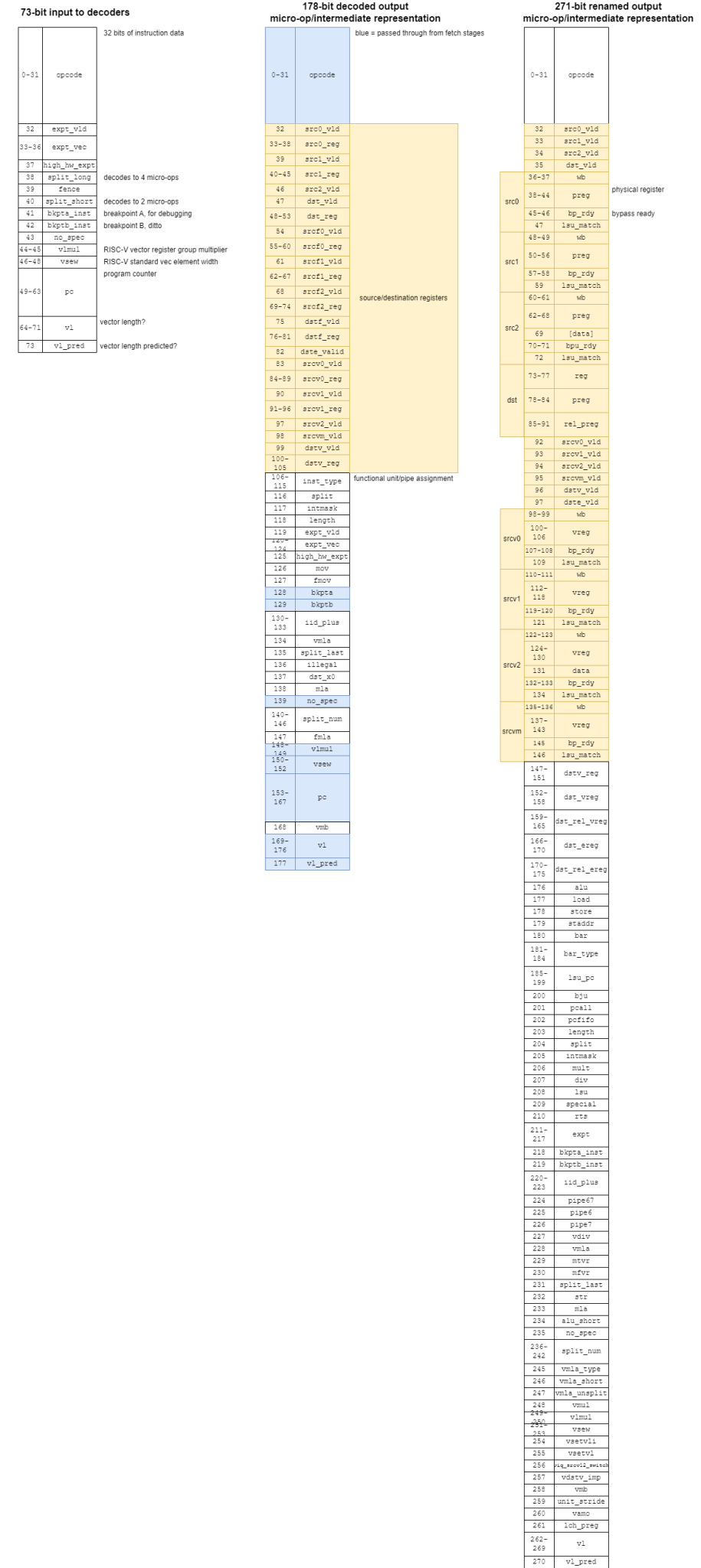
C910’s instruction rename (IR) stage then checks for matches between architectural registers to find inter-instruction dependencies. It then assigns free registers out of the respective pool (integer or FP registers), or by picking newly deallocated registers coming off the retire stage. The IR stage does further decoding too. Instructions are further labeled with whether they’re a multi-cycle ALU operation, which ports they can go to, and so on. After renaming, micro-ops are 271 bits.

From software, C910’s frontend can sustain 3 instructions per cycle as long as code fits within the 64 KB instruction cache. L2 code bandwidth is low at under 1 IPC. SiFive’s P550 offers more consistent frontend bandwidth for larger code footprints, and can maintain 1 IPC even when running code from L3.
Out-of-Order Execution Engine
C910’s backend uses a physical register file (PRF) based out-of-order execution scheme, where both pending and known-good instruction results are stored in register files separate from the ROB. C910’s source code (ct_rtu_rob.v) defines 64 ROB entries, but T-HEAD’s paper says the ROB can hold up to 192 instructions. Microbenchmarking generally agrees.

Therefore, C910 has reorder buffer capacity on par with Intel’s Haswell from 2013, theoretically letting it keep more instructions in flight than P550 or Goldmont Plus. However, other structures are not appropriately sized to make good use of that ROB capacity.

RISC-V has 32 integer and 32 floating point registers, so 32 entries in each register file generally have to be reserved for holding known-good results. That leaves only 64 integer and 32 floating point registers to hold results for in-flight instructions. Intel’s Haswell supports its 192 entry ROB with much larger register files on both the integer and floating point side.
Execution Units
C910 has eight execution ports. Two ports on the scalar integer side handle the most common ALU operations, while a third is dedicated to branches. C910’s integer register file has 10 read ports to feed five execution pipes, which includes three pipes for handling memory operations. A distributed scheduler setup feeds C910’s execution ports. Besides the opcode and register match info, each scheduler entry has a 7-bit age vector to enable age-based prioritization.

Scheduler capacity is low compared to Goldmont Plus and P550, with just 16 entries available for the most common ALU operations. P550 has 40 scheduler entries available across its three ALU ports, while Goldmont Plus has 30 entries.
C910’s FPU has a simple dual pipe design. Both ports can handle the most common floating point operations like adds, multiplies, and fused multiply. Both pipes can handle 128-bit vector operations too. Feeding each port requires up to four inputs from the FP/vector register file. A fused multiply instruction (a*b+c) requires three inputs. A fourth input provides a mask register. Unlike AVX-512 and SVE, RISC-V doesn’t define separate mask registers, so all inputs have to come from the FP/vector register file. Therefore, C910’s FP register file has almost as many read ports as the integer one, despite feeding fewer ports.

Floating point execution latency is acceptable, and ranges from 3 to 5 cycles for the most common operations. Some recent cores like Arm’s Cortex X2, Intel’s Golden Cove, and AMD’s Zen 5 can do FP addition with 2 cycle latency. I don’t expect that from a low power core though.

Memory Subsystem
Two address generation units (AGUs) on C910 calculate effective addresses for memory accesses. One AGU handles loads, while the other handles stores. C910’s load/store unit is generally split into two pipelines, and aims to handle up to one load and one store per cycle. Like many other cores, store instructions are broken into a store address and a store data micro-op.

39-bit virtual addresses are then generated into 40-bit physical addresses. C910’s L1 DTLB has 17 entries and is fully associative. A 1024 entry, 4-way L2 TLB handles L1 TLB misses for both data and instruction accesses, and adds 4 cycles latency over a L1 hit. Physically, the L2 TLB has two banks, both 256×84 SRAM instances. The tag array is a 256×196 bit SRAM instance, and a 196-bit access includes tags for all four ways along with four “FIFO” bits, possibly used to implement a FIFO replacement policy. Besides necessary info like the virtual page number and a valid bit, each tag includes an address space ID and a global bit. These can exempt an entry from certain TLB flushes, reducing TLB thrashing on context switches. In total, the L2 TLB’s tags and data require 8.96 KB of bit storage.

Physical addresses are written into the load and store queues, depending on whether the address is a load or store. I’m not sure how big the load queue is. C910’s source code suggests there are 12 entries, and microbenchmarking results are confusing.

In the source code, each load queue entry stores 36 bits of the load’s physical address along with 16 bits to indicate which bits are valid, and a 7-bit instruction id to ensure proper ordering. A store queue entry stores the 40-bit physical address, pending store data, 16 byte valid bits, a 7-bit instruction id, and a ton of other fields. To give some examples:
wakeup_queue: 12 bits, possibly indicates which dependent loads should be woken up when data is ready
sdid: 4 bits, probably store data id
age_vec, age_vec_1: 12 bit age vectors, likely for tracking store order
To check for memory dependencies, the load/store unit compares bits 11:4 of the memory address. From software testing, C910 can do store forwarding for any load completely contained within the store, regardless of alignment within the store. However, forwarding fails if a load crosses a 16B aligned boundary, or a store crosses a 8B aligned boundary. Failed store forwarding results in a 20+ cycle penalty.
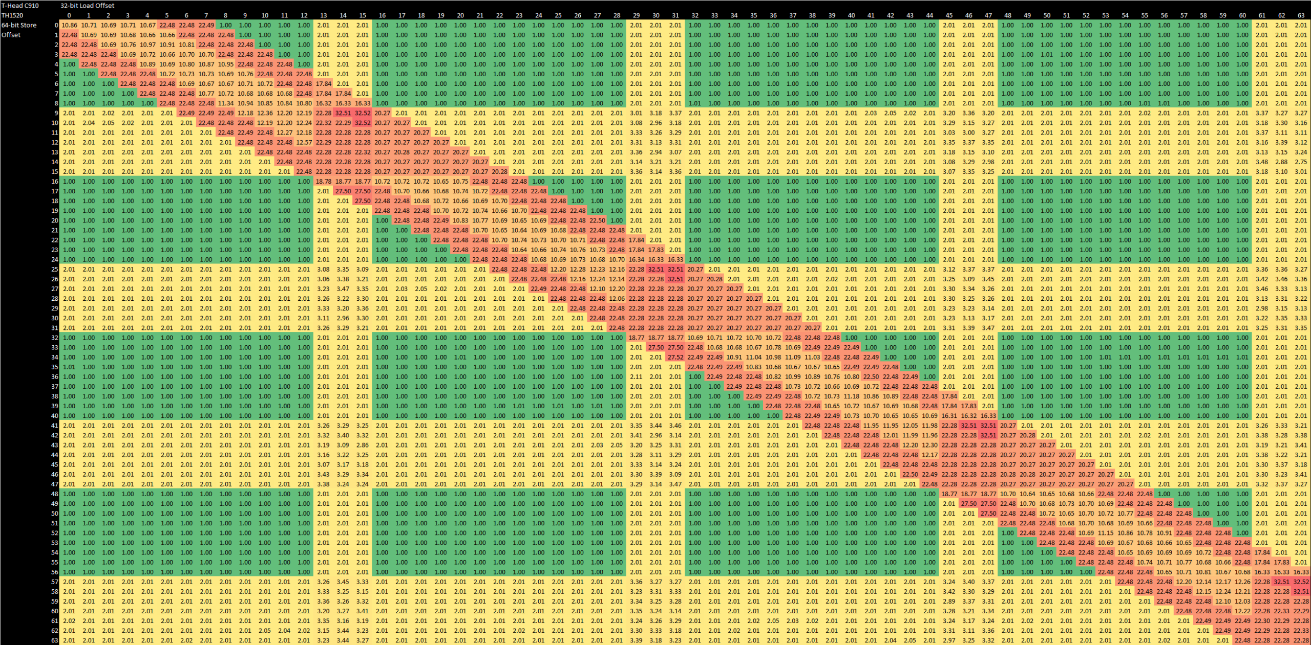
C910 handles unaligned accesses well, unlike P550. If a load doesn’t cross a 16B boundary or a store doesn’t cross a 8B boundary, it’s basically free. If you do cross those alignment boundaries, you don’t face a performance penalty beyond making an extra L1D access under the hood. Overall, C910’s load/store unit and forwarding behavior is a bit short of the most recent cores from Intel and AMD. But it’s at about the same level as AMD’s Piledriver, a very advanced and high performance core in its own right. That’s a good place to be.
Data Cache
The 64 KB, 2-way data cache has 3 cycle latency, and is divided into 4 byte wide banks. It can handle up to one load and one store per cycle, though 128-bit stores take two cycles. L1D tags are split into two separate arrays, one for loads and one for stores.

Data cache misses are tracked by one of eight line-fill buffer entries, which store the miss address. Refill data is held in two 512-bit wide fill buffer registers. Like the instruction cache, the data cache uses a simple FIFO replacement policy.
L2 Cache and Interconnect
Each C910 core interfaces with the outside world via a “PIU”, or processor interface unit. At the other end, a C910 cluster has a Consistency Interface Unit (CIU) that accepts requests from up to four PIUs and maintains cache coherency. The CIU is split into two “snb” instances, each of which has a 24 entry request queue. SNB arbitrates between requests based on age, and has a 512-bit interface to the L2 cache.
C910’s L2 cache acts as both the first stop for L1 misses and as a cluster-wide shared last level cache. On the TH1520, it has 1 MB of capacity and is 16-way set associative with a FIFO replacement policy. To service multiple accesses per cycle, the L2 is built from two banks, selected by bit 6 of the physical address. The L2 is inclusive of upper level caches, and uses ECC protection to ensure data integrity.

L2 latency is 60 cycles which is problematic for a core with limited reordering capacity and no mid-level cache. Even P550’s 4 MB L3 cache has better latency than C910’s L2, from both a cycle count and true latency standpoint. Intel’s Goldmont Plus also uses a shared L2 as a last level cache, and has about 28 cycles of L2 latency (counting a uTLB miss).

C910’s L2 bandwidth also fails to impress. A single core gets just above 10 GB/s, or 5.5 bytes per cycle. All four cores together can read from L2 at 12.6 GB/s, or just 1.7 bytes per cycle per core. Write bandwidth is better at 23.81 GB/s from all four cores, but that’s still less than 16 bytes per cycle in total, and writes are usually less common than reads.
Again, C910’s L2 is outperformed by both P550’s L3 and Goldmont Plus’s L2. I suspect multi-threaded applications will easily push C910’s L2 bandwidth limits.
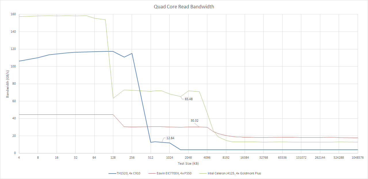
Off-cluster requests go through a 128-bit AXI4 bus. In the Lichee Pi 4A, the TH1520 has just under 30 GB/s of theoretical DRAM bandwidth from its 64-bit LPDDR4X-3733 interface. Achieved read bandwidth is much lower. Multithreaded applications might find 4.2 GB/s a bit tight, especially when there’s only 1 MB of last level cache shared across four cores.

DRAM latency is at least under control at 133.9 ns, tested using 2 MB pages and 1 GB array. It’s not on the level of a desktop CPU, but it’s better than Eswin and Intel’s low power implementations.
Core to Core Latency
Sometimes, the memory subsystem has to carry out a core to core transfer to maintain cache coherency. Sites like Anandtech have used a core to core latency test to probe this behavior, and I’ve written my own version. Results should be broadly comparable with those from Anandtech.
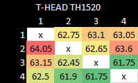
T-HEAD’s CIU can pass data between cores with reasonable speed. It’s much better than P550, which saw over 300 ns of latency within a quad core cluster.
Final Words
C910 is T-HEAD’s first out-of-order core. Right out of the gate, C910 is more polished than P550 in some respects. Core to core latency is better, unaligned accesses are properly handled, and there’s vector support. Like P550, C910 aims to scale across a broad range of low power applications. L2 capacity can be configured up to 8 MB, and multi-cluster setups allow scaling to high core counts. I feel like there’s ambition behind C910, since Alibaba wants to use in-house RISC-V cores instead of depending on external factors.
Alibaba has been promoting Xuantie core IP series to facilitate external customers for edge computing applications, such as AI, edge servers, industrial control and advanced driver assistance systems (ADAS)…by the end of 2022, a total volume of 15 million units is expected
Xuantie-910: A Commercial Multi-Core 12-Stage Pipeline Out-of-Order 64-bit High Performance RISC-V Processor with Vector Extension – T-Head Division, Alibaba Cloud
Yet I also feel the things C910 does well are overshadowed by executing poorly on the basics. The core’s out-of-order engine is poorly balanced, with inadequate capacity in critical structures like the schedulers and register files in relation to its ROB capacity. CPU performance is often limited by memory access performance, and C910’s cache subsystem is exceptionally weak. The cluster’s shared L2 is both slow and small, and the C910 cores have no mid-level cache to insulate L1 misses from that L2. DRAM bandwidth is also lackluster.
C910 is therefore caught in a position where it needs to keep a lot of instructions in flight to smooth out spikes in demand for memory bandwidth and mitigate high L2 latency, but can rarely do so in practice because its ROB capacity isn’t supported by other structures. C910’s unaligned access handling, vector support, and decent core-to-core latency are all nice to have. But tackling those edge cases is less important than building a well balanced core supported by a solid memory subsystem. Missing the subset of applications that use unaligned accesses or take advantage of vectorization is one thing. But messing up performance for everything else is another. And C910’s poor L2 and DRAM performance may even limit the usefulness of its vector capabilities, because vectorized applications tend to pull more memory bandwidth.
Hopefully T-HEAD will use experience gained from C910 to build better cores going forward. With Alibaba behind it, T-HEAD should have massive financial backing. I also hope to see more open source out-of-order cores going forward. Looking through C910 source code was very insightful. I appreciated being able to see how micro-op formats changed between pipeline stages, and how instruction decode is split across several stages that aren’t necessarily labeled “decode”.
If you like the content then consider heading over to the Patreon or PayPal if you want to toss a few bucks to Chips and Cheese. Also consider joining the Discord.
I adore your content. Just got excited when I heard my phone ding and saw it was this new article:D
Th anks, nice follow up article on RISC-V CPUs. I wonder how many of these four core cluster Xuanties can be combined in one CPU? In other words, are there large manycore CPUs based on this? Thanks!