
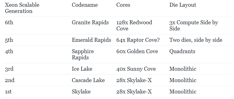
A Look into Intel Xeon 6’s Memory Subsystem

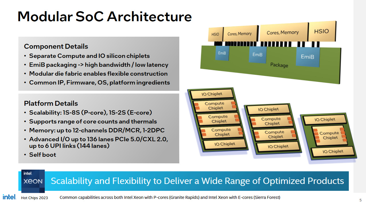
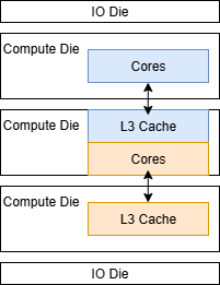
Intel’s server dominance has been shaken by high core count competition from the likes of AMD and Arm. Xeon 6, Intel’s latest server platform, aims to address this with a more scalable chiplet strategy. Chiplets are now arranged side by side, with IO chiplets on either side of the chip. It’s reminiscent of the arrangement Huawei used for Kunpeng 920, but apparently without the uniform chiplet height restrictions of Huawei’s design. Intel also scales up to three compute dies, as opposed to a maximum of two on Kunpeng 920.
Compared to Emerald Rapids and Granite Rapids, Xeon 6 uses a more aggressive chiplet strategy. Lower speed IO and accelerators get moved to separate IO dies. Compute dies contain just cores and DRAM controllers, and use the advanced Intel 3 process. The largest Xeon 6 SKUs incorporate three compute dies and two IO dies, scaling up to 128 cores per socket. It’s a huge core count increase from the two prior generations.
AWS has Xeon 6 instances generally available with their r8i virtual machine type, providing an opportunity to check out Intel’s latest chiplet design from a software performance perspective. This will be a short look. Renting a large cloud instance for more detailed testing is prohibitively expensive.
System Overview
AWS’s r8i instance uses the Xeon 6 6985P-C. This SKU is not listed on Intel’s site or other documentation, so a brief overview of the chip is in order. The Xeon 6 6985P-C has 96 Redwood Cove cores that clock up to 3.9 GHz, and each have 2 MB of L2 cache. Redwood Cove is a tweaked version of Intel’s Golden Cove/Raptor Cove, and has previously featured on Intel’s Meteor Lake client platform. Redwood Cove brings a larger 64 KB L1 instruction cache among other improvements discussed in another article. Unlike their Meteor Lake counterparts, Xeon 6’s Redwood Cove cores enjoy AVX-512 support with 2x 512-bit FMA units, and 2x512-bit load + 1x512-bit store throughput to the L1 data cache. AMX support is present as well, providing specialized matrix multiplication instructions to accelerate machine learning applications.
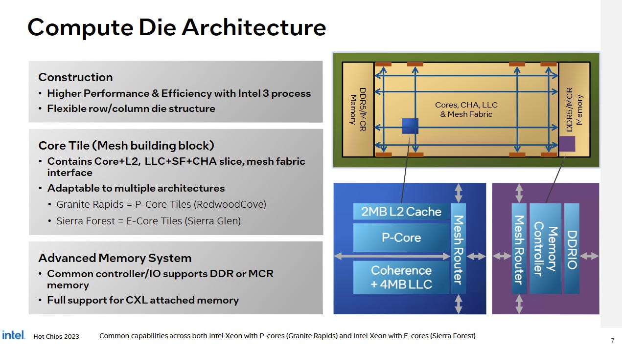
Xeon 6 uses a mesh interconnect like prior Intel server chips. Cores share a mesh stop with a CHA (Caching/Home Agent), which incorporates a L3 cache slice and a snoop filter. The Xeon 6 6985P-C has 120 CHA instances running at 2.2 GHz, providing 480 MB of total L3 across the chip. CHA count interestingly doesn’t match enabled core count. Intel may be able to harvest cores without disabling the associated cache slice, as they had to do on some older generations.
The mesh runs across die boundaries to keep things logically monolithic. Modular Data Fabric (MDF) mesh stops sit at die edges where dies meet with their neighbors. They handle the logical layer of the mesh protocol, much like how IFOP blocks on AMD chips encode the Infinity Fabric protocol for transport between dies. The physical signals on Xeon 6 run over Intel’s EMIB technology, which uses an embedded silicon bridge between dies. The Xeon 6 6985P-C has 80 MDF stops running at 2.5 GHz. Intel hasn’t published documents detailing Xeon 6’s mesh layout. One possibility is that 10 MDF stops sit at each side of a die boundary.
Intel places memory controllers at the short edge of the compute dies. The largest Xeon 6 SKUs have 12 memory controllers, or four per compute die. The Xeon 6 6985P-C falls into that category. AWS equipped the Xeon 6 6985P-C with 1.5 TB of Micron DDR5-7200 per socket. I couldn’t find the part number (MTC40F2047S1RC72BF1001 25FF) anywhere, but it’s certainly very fast DDR5 for a server platform. AWS has further configured the chip in SNC3 mode. SNC stands for sub-NUMA clustering, and divides the chip into three NUMA nodes. Doing so partitions the physical address space into three portions, each backed by the DRAM controllers and L3 cache on their respective compute dies. That maintains affinity between the cores, cache, and memory controllers on each die, reducing latency as long as cores access the physical memory backed by memory controllers on the same die. Xeon 6 also supports a unified mode where all of the attached DRAM is exposed in one NUMA node, with accesses striped across all of the chip’s memory controllers and L3 slices. However, SNC3 mode is what AWS chose, and is also Intel’s default mode.
Cache and Memory Latency
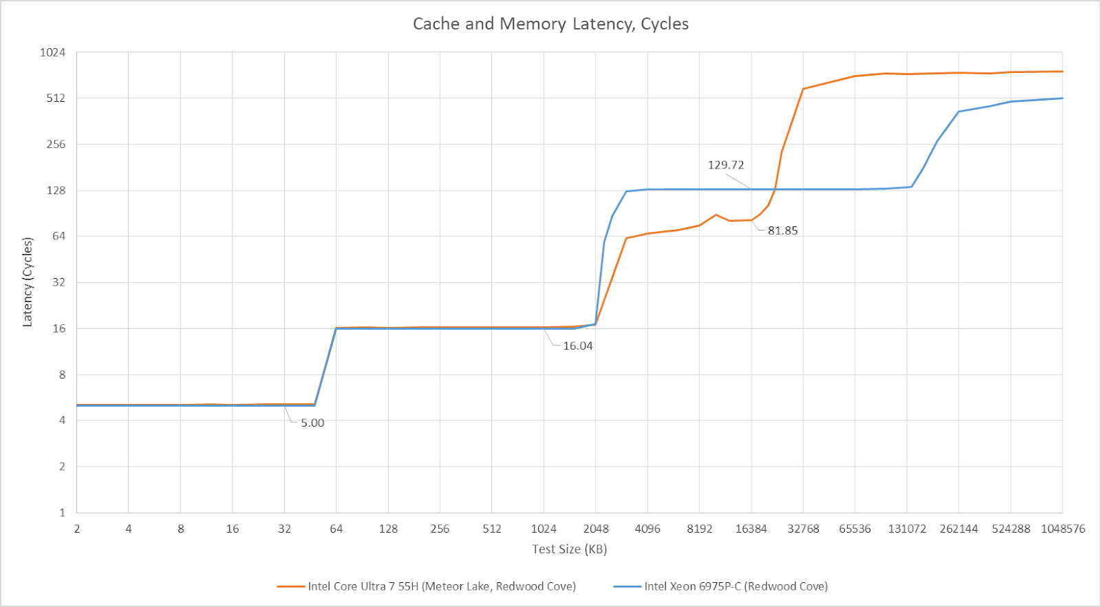
Xeon 6’s Redwood Cove cores have the same 5 cycle L1D and 16 cycle L2 latencies as their Meteor Lake counterparts, though the server part’s lower clock speeds mean higher actual latencies. Memory subsystem characteristics diverge at the L3 cache, which has a latency of just over 33 ns (~130 cycles). In exchange for higher latency, each core is able to access a huge 160 MB pool of L3 cache on its tile.
L3 latency regresses slightly compared to Emerald Rapids. It’s concerning because the Emerald Rapids Xeon Platinum 8559C chips in AWS’s i7i instances do not use SNC. Thus each core in Emerald Rapids sees the full 320 MB of L3 as a logically monolithic cache, and L3 accesses are distributed across both chiplets. The same applies to DRAM accesses. Emerald Rapids achieves lower latency to its DDR5-5600 Hynix memory (HMCGM4MGBRB240N).
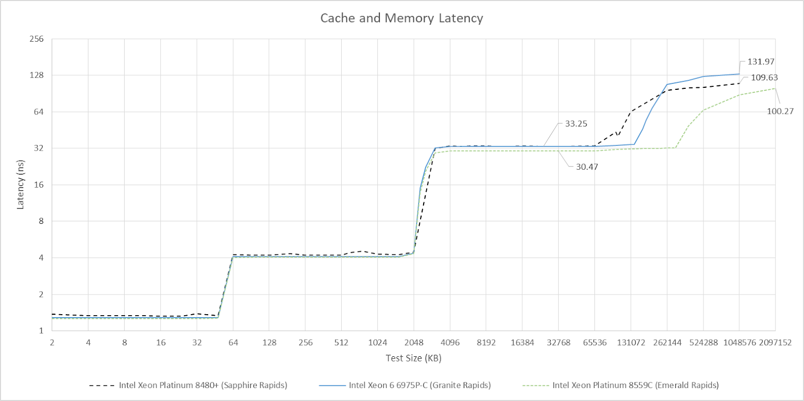
Compared to Sapphire Rapids, Xeon 6’s L3 is a straightforward upgrade with higher capacity at similar latency. DRAM latency is still a bit worse on Xeon 6 though. Note: I originally mentioned MCRDIMM support here. From the DIMM part number above, AWS isn’t using MCRDIMMs so they’re not relevant to results in this article.
Next to AMD’s Zen 5 server platform, codenamed Turin, Xeon 6 continues to use larger but slower caches. Intel’s large L2 helps mitigate L3 latency, letting Intel use a larger L3 shared across more cores. AMD’s L3 is higher performance, but is also smaller and only shared across eight cores. That translates to less efficient SRAM capacity usage across the chip, because data may be duplicated in different L3 cache instances. For low threaded workloads, AMD may also be at a disadvantage because a single core can only allocate into its local 32 MB L3 block, even though the chip may have hundreds of megabytes of total L3. Even if AMD extends each CCD’s L3 with 3D stacking (VCache), 96 MB is still less than Intel’s 160 MB.
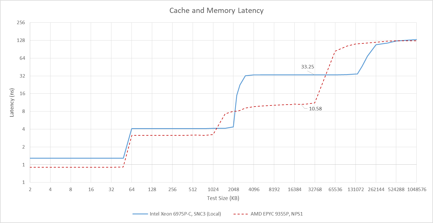
Memory latency on AMD’s platform is 125.6 ns, higher than Emerald Rapids but better than Xeon 6. For this test, the AMD system was set up in NPS1 mode, which distributes accesses across all of the chip’s 12 memory controllers. It’s not the most latency optimized mode, and it’s concerning that AMD achieves better memory latency without having to contain memory accesses in smaller divisions.
Bandwidth
Xeon 6’s core-private caches provide high bandwidth with AVX-512 loads. A single core has about 30 GB/s of L3 bandwidth, just under what Emerald Rapids could achieve. A read-modify-write pattern nearly doubles L3 bandwidth, much like it does on AMD’s Zen line. On Zen, that’s due to implementation details in the L3’s victim cache operation. A L3 access request can come with a L2 victim, and thus perform both a read and a write on the L3. That doubles achievable bandwidth with the same request rate. Intel may have adopted a similar scheme, though figuring that out would require a more thorough investigation. Or, Intel may have independent queues for pending L3 lookups and writebacks. Zooming back up, Zen 5 achieves high L3 bandwidth at the cost of smaller L3 instances shared across fewer cores. It’s the same story as with latency.
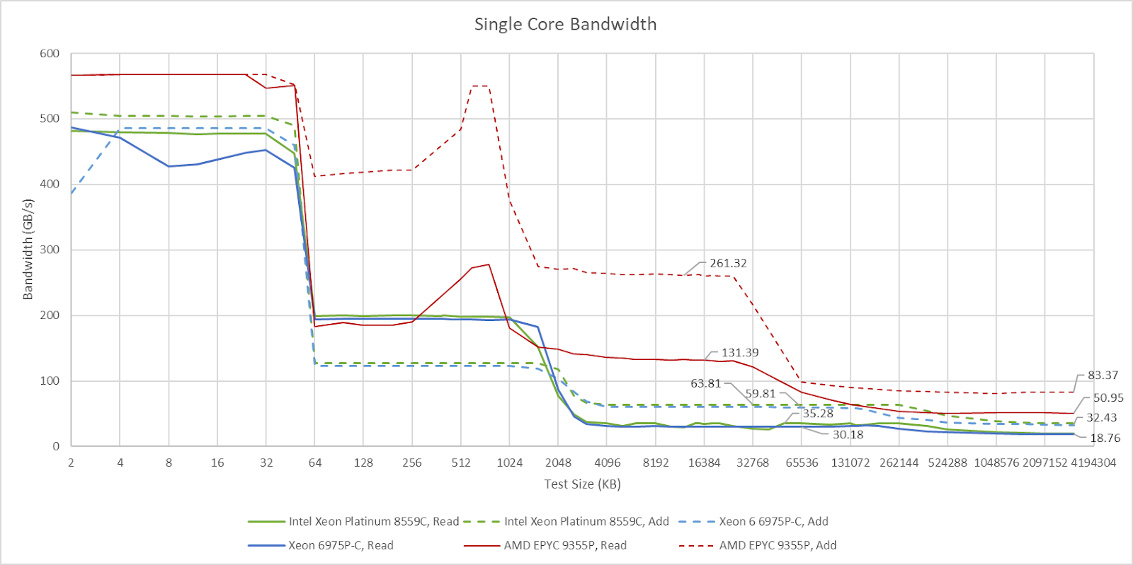
DRAM bandwidth from a single Xeon 6 core comes in at just below 20 GB/s. It’s lower than on Zen 5, but also less of a concern thanks to massive L3 capacity. As with L3 bandwidth, a read-modify-write pattern dramatically increases DRAM bandwidth achievable from a single core.
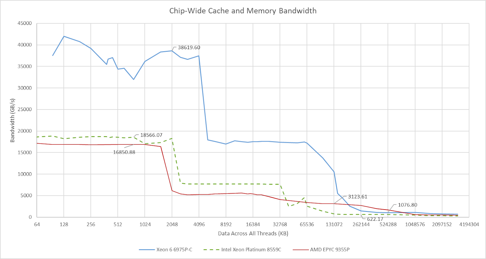
At the chip level, Xeon 6’s high core count and fast L1/L2 caches can provide massive bandwidth for code with good memory access locality. Total cache read bandwidth is a huge step above Emerald Rapids and smaller Zen 5 SKUs that prioritize per-core performance over throughput. Xeon 6’s L3 bandwidth improves to align with its core count increase, though L3 bandwidth in total remains behind AMD.
With each thread reading from memory backed by its local NUMA node, I got 691.62 GB/s of DRAM bandwidth. It’s a step ahead of Emerald Rapids’s 323.45 GB/s. Intel has really scaled up their server platform. Xeon 6’s 12 memory controllers and faster memory give it a huge leg up over Emerald Rapids’s eight memory controllers. AMD also uses 12 memory controllers, but the EPYC 9355P I had access to runs DDR5-5200, and achieved 478.98 GB/s at the largest test size using a unified memory configuration (single NUMA node per socket).
NUMA/Chiplet Characteristics
Intel uses consistent hashing to route physical addresses to L3 cache slice (CHAs), which then orchestrate coherent memory access. Xeon 6 appears to carry out this consistent hashing by distributing each NUMA node’s address space across L3 slices on the associated die, as opposed to covering the entire DRAM-backed physical address space with the CHAs on each die. Thus accesses to a remote NUMA node are only cached by the remote die’s L3. Accessing the L3 on an adjacent die increases latency by about 24 ns. Crossing two die boundaries adds a similar penalty, increasing latency to nearly 80 ns for a L3 hit.
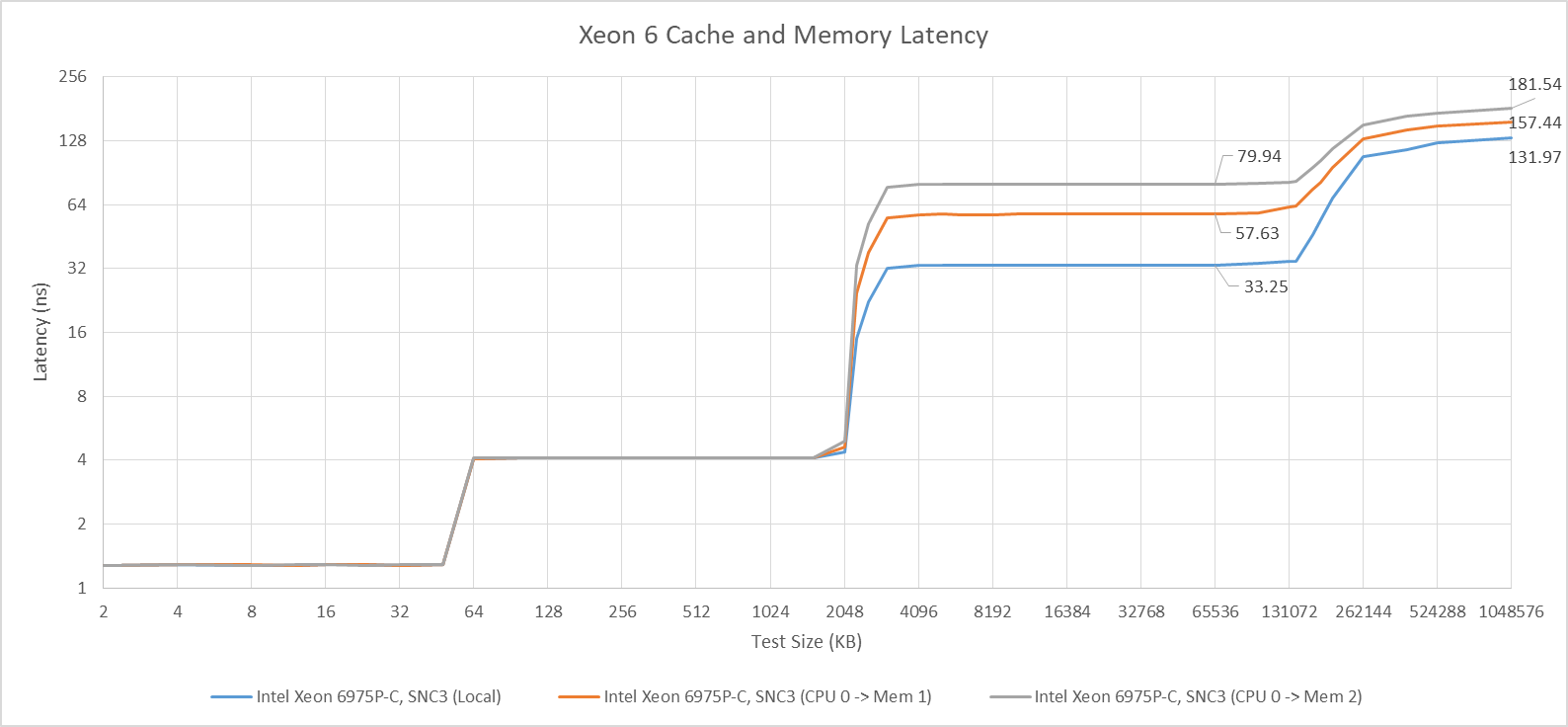
Similar penalties apply to remote DRAM accesses, though that’s to be expected for any NUMA setup. Getting data from memory controllers across one die boundary takes 157.44 ns, for about 26 ns extra over hitting a local one. Crossing two die boundaries adds another 25 ns, bringing latency to 181.54 ns.
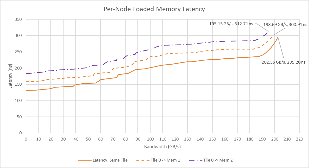
Under load, latency gradually increases until it reaches a plateau, before seeing a sharper rise as the test approaches DRAM bandwidth limits. It’s not a perfect hockey stick pattern like on some other chips. Latency remains reasonably well controlled, at just under 300 ns for a within-NUMA-node access under high bandwidth node. Crossing tile boundaries increases latency, but leaves bandwidth largely intact. Repeating the exercise with 96 MB used for bandwidth test threads and 16 MB for the latency test gives an idea of what cross-die L3 bandwidth is like. It’s very high. Cross-die bandwidth nearly reaches 500 GB/s for a read-only pattern.
I was able to exceed 800 GB/s of cross-die bandwidth by respecting Intel’s conga line topology, for lack of a better term. Specifically, I had cores from node 0 accessing L3 on node 1, and cores on node 1 accessing L3 on node 2. I used a read-modify-write pattern as well to maximize L3 bandwidth. It’s a rather contrived test, but it underscores the massive cross-die bandwidth present in Intel’s Xeon 6 platform. A single Xeon 6 compute die has more off-die bandwidth than an AMD CCD, even when considering GMI-Wide AMD setups that use two Infinity Fabric links between each CCD and the central IO die. However, each AMD L3 instance covers the physical address space across all NUMA nodes, so the situations aren’t directly comparable.
Coherency Latency
The memory subsystem may have to orchestrate transfers between peer caches, which I test by bouncing a value between two cores. That “core to core latency” shows similar characteristics to prior Xeon generations. Transfers within a compute die land in the 50-80 ns range, with only a slight increase when crossing die boundaries. NUMA characteristics above apply here too. I ran this test with memory allocated out of the first NUMA node.
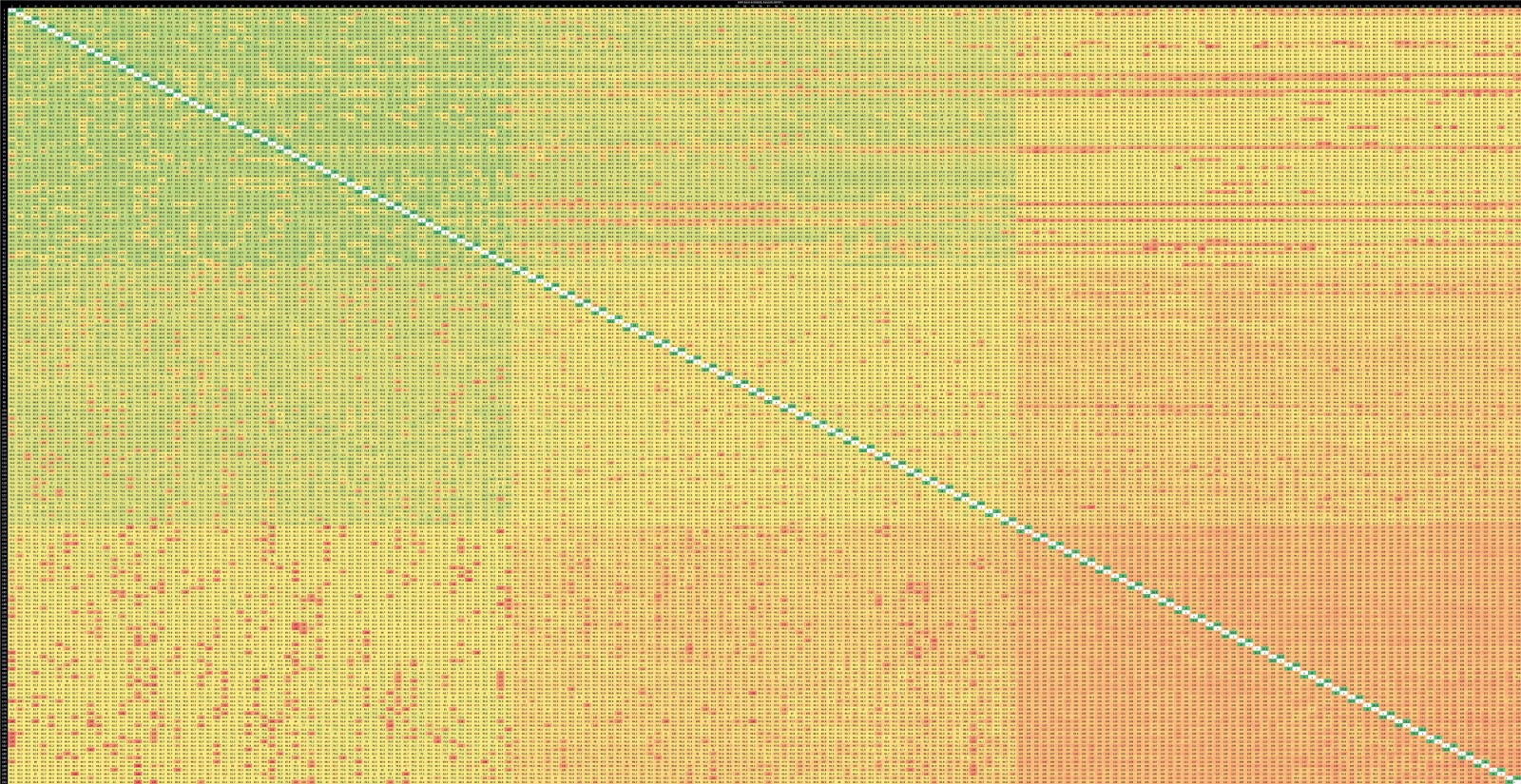
A pair of cores on NUMA node 2 would need a CHA on node 0 to orchestrate the transfer, which is why nodes farther away from the first compute die show higher latency in this test. The worst case of 100-120 ns with cores going through a CHA on the farthest NUMA node is still better than the 150-180 ns on AMD server platforms when crossing cluster (CCX) boundaries. In both cases, the round trip goes across two die boundaries. But Intel’s logically monolithic topology and advanced packaging technologies likely give it a lead.
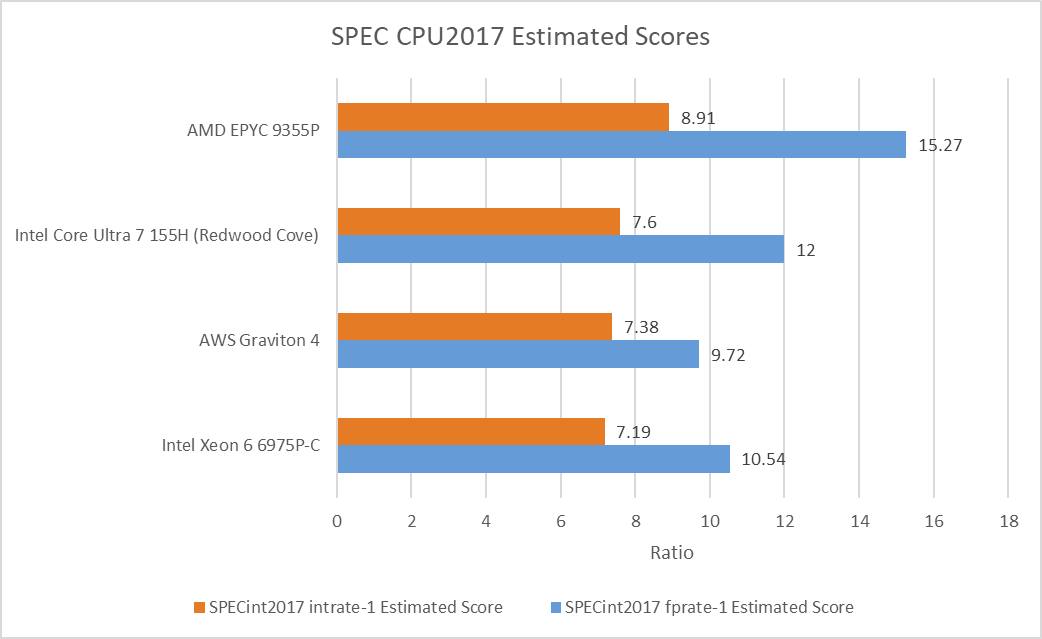
Single Core Performance: SPEC CPU2017
SPEC CPU2017 is an industry standard benchmark, and I’ve been running the rate suite with a single copy to summarize single-thread performance. This 96 core Xeon 6 part falls behind lower core count chips that are better optimized for per-core performance. Its score in the integer suite is closely matched to AWS’s Graviton 4, which similarly implements 96 cores per socket. Xeon 6 enjoys a slight 8.4% lead over Graviton 4 in the floating point suite.
Final Words
Intel’s latest server chiplet strategy is superficially similar to AMD’s. Both use compute and IO dies. Both strive for a scalable and modular design that can scale across a range of core counts. But Intel and AMD have very different system level design philosophies, driving huge architectural differences under the hood. Intel wants to present a logically monolithic chip, and wants their mesh to accommodate an ever increasing number of agents. It’s not an easy task, because it demands very high performance from cross-die transfers.
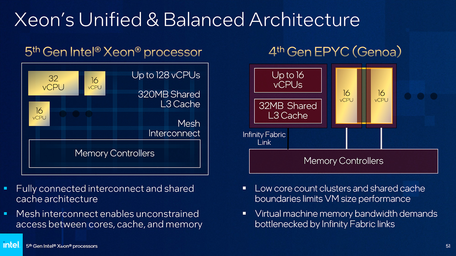
AMD in contrast doesn’t try to make a big system feel monolithic, and instead goes with two interconnect levels. A fast intra-cluster network handles high speed L3 traffic and presents the cluster as one client to Infinity Fabric. Infinity Fabric only handles DRAM and slower IO traffic, and thus faces a less demanding job than Intel’s mesh. Infinity Fabric does cross die boundaries, but gets by with on-package traces thanks to its lower performance requirements.
Intel’s approach has advantages, even when subdivided using SNC3 mode. These include a more unified and higher capacity L3 cache, better core to core latency, and no core cluster boundaries with bandwidth pinch points. And theoretically, placing memory controllers on compute dies allows SNC3 mode to deliver lower DRAM latency by avoiding cross-die hops.
But every design comes with tradeoffs. The DRAM latency advantage doesn’t materialize against AMD’s Turin. L3 performance isn’t great. Latency is high, and a Redwood Cove core has less L3 bandwidth than a Zen 5 core does from DRAM. I have to wonder how well the L3 would perform in a Xeon 6 chip configured to run as a single NUMA node too. L3 accesses would start with a baseline latency much higher than 33 ns. Getting hard numbers would be impossible without access to a Xeon 6 chip in such a configuration, but having 2/3 of accesses cross a die boundary would likely send latency to just under 50 ns. That is, (2 * 57.63 + 33.25) / 3 = 49.5 ns. Scalability is another question too. Extending the conga line with additional compute dies may erode Intel’s advantage of crossing fewer die boundaries on average than AMD. The best way to keep scaling within such a topology would likely be increasing core counts within each die, which could make it harder to scale to smaller configurations using the same dies.
I wonder if keeping a logically monolithic design is worth the tradeoffs. I’m not sure if anyone has built a mesh this big, and other large meshes have run into latency issues even with techniques like having core pairs share a mesh stop. Nvidia’s Grace for example uses a large mesh and sees L3 latency reach 38.2 ns. Subdividing the chip mitigates latency issues but starts to erode the advantages of a logically monolithic setup. But of course, no one can answer the question of whether the tradeoffs are worthwhile except the engineers at Intel. Those engineers have done a lot of impressive things with Xeon 6. Going forward, Intel has a newer Lion Cove core that’s meant to compete more directly with Zen 5. Redwood Cove was more contemporary with Zen 4. I look forward to seeing what Intel does at the system level with their next server design. Those engineers are no doubt busy cooking it up.
Great article! Although I believe ice lake has up to 40 cores, not 28 :P
For AI workload on the cloud say when pair with Google TPU pods like hardwares, which form of interconnect best suit AI related workloads?
Mesh (Granite Rapids) or "semi-mesh like" (Turing)
And does AI workload tend to favour XEON CPU, because of the onboard accelerators and all cores are connected via a mesh?