
AMD’s Instinct MI455X: Aiming for the Sun


Editor’s Note (7/25/2026): The article has been edited with more information about the L2 behavior along with the bandwidth of the die to die interface.
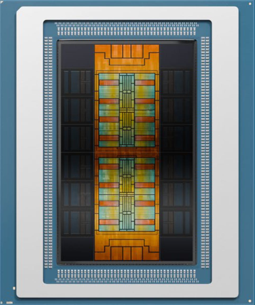
Hello you fine Internet folks, here at AMD’s Advancing AI event we are looking at AMD’s brand new Instinct MI455X, replacing the older Instinct MI355X at the top of their AI stack. It is AMD’s first GPU designed for rack-scale AI deployments and is based on the new CDNA5 architecture with major changes to the compute unit and SoC, including enhancements to compute performance, improved memory bandwidth, larger memory capacity, and packaged using TSMC’s CoWoS-L.
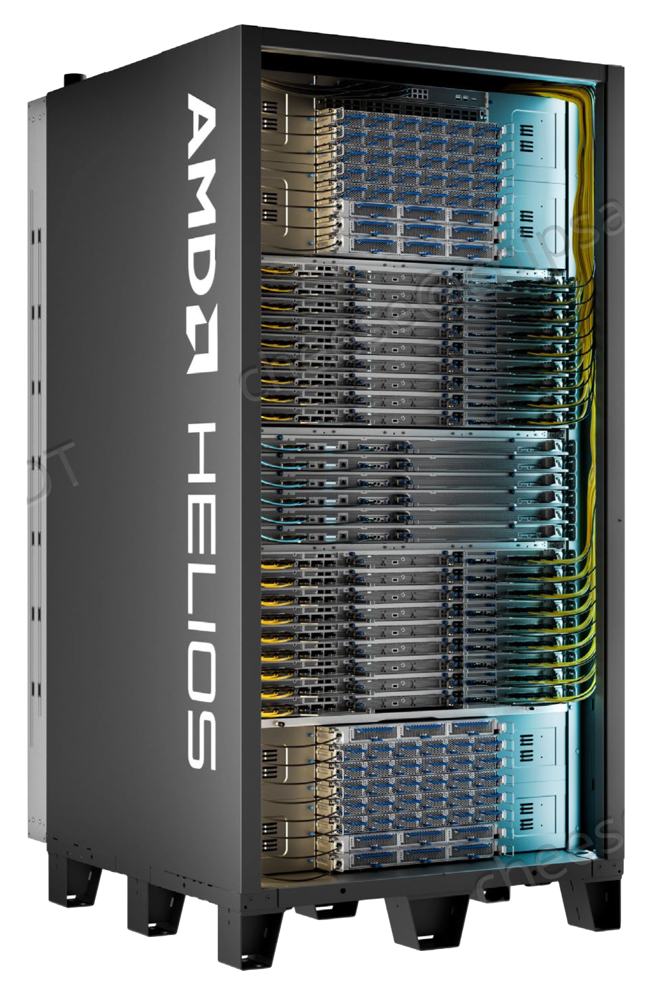
It comes along with the new Helios rackscale solution, enabling scaling to 72 GPUs in a single pod, up from 8 GPUs for previous MI355X systems. It also features a new fault-tolerant scale-up networking architecture based on UALink over Ethernet (UALoE) with single-hop all-to-all communication across the entire rack.
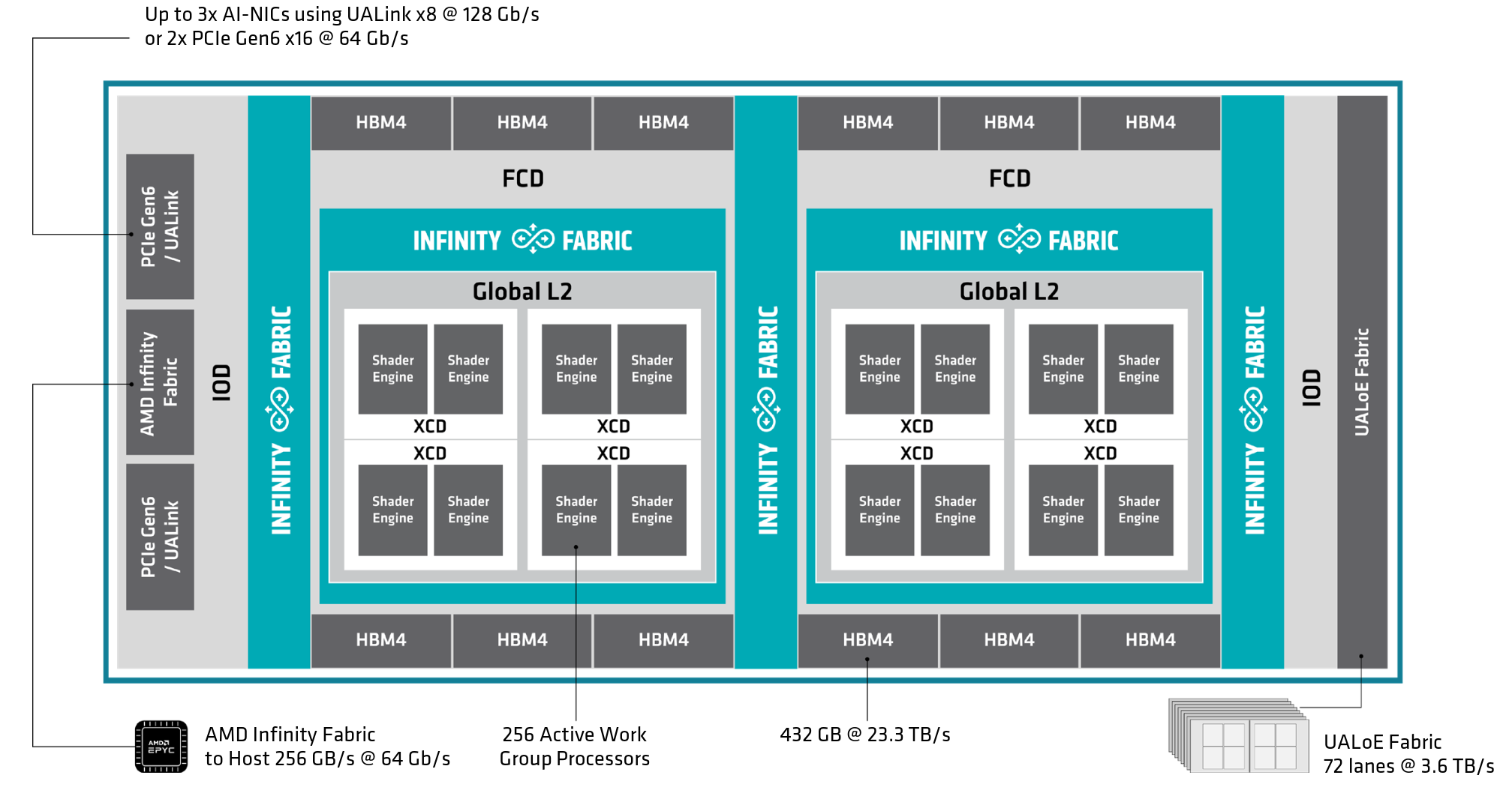
A single MI455X contains 256 Work Group Processors (WGPs) across 8 Accelerator Complex Dies (XCDs), with a max “engine” clock of 2.4GHz. This enables peak compute figures ranging from 315 TFLOP for matrix/vector FP32 and vector FP16, and up to 40.26 PFLOP for OCP MXFP4. This is paired with 12 stacks of HBM4 each on a 2048 bit bus for a total of 192 channels, giving each GPU a total of 432 GB of memory at 23.3 TB/sec.
CU/WGP changes
Starting with the changes in the “Compute Unit”, AMD now counts the WGPs instead of the CUs for CDNA5. Unlike what they have done on their consumer counterparts where each WGP counts as two CUs.
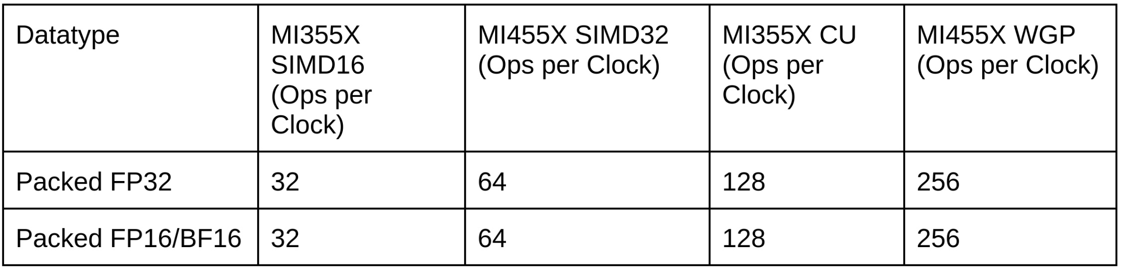
But just like RDNA4, each WGP comprises four dual issue Wave32 SIMD32 units alongside 4 scalar units which is a massive change from CDNA4’s four single issue Wave64 SIMD16 units.
This means that each WGP can do up to 256 packed FP32 operations per cycle (512 FLOPS if using FMA).
To support this new SIMD design, the VGPR register file has been reorganized with any wave now able to address up to 1,024 VGPRs which is four times the number of VGPRs that a wave could access in prior CDNA and RDNA architectures. Each SIMD still has 128kB of vector registers just like CDNA4 which means it has twice as many (1024) registers available in practice due to Wave32 vs Wave64, but it is still less than the 192kB available on RDNA4. It also means that a single wavefront is in some cases expected to occupy the entire SIMD.
The matrix units also have been beefed up with each matrix unit being able to do up to 8,192 FP4 operations per cycle and with 4 matrix units per WGP you can do up to 65,536 matrix operations per cycle per WGP.
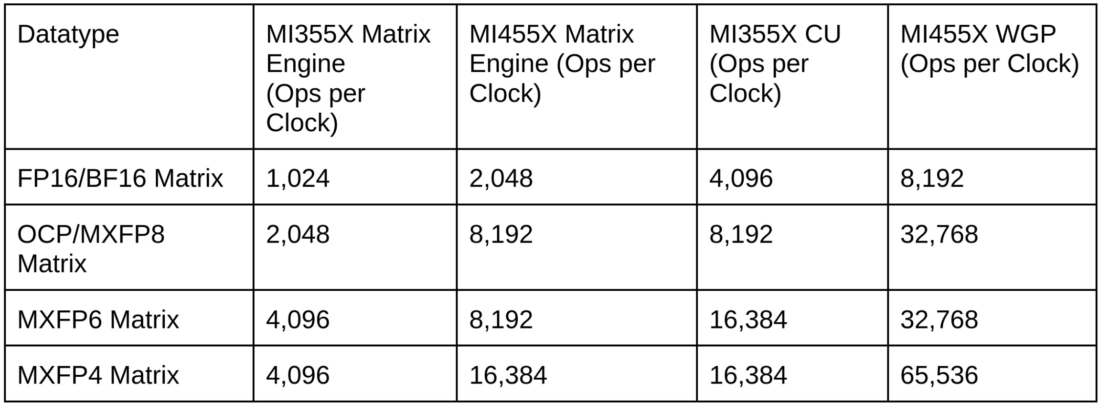
This means that only FP4 and FP8 are practically faster in the new architecture, and the rest of the performance comes from increasing the SIMD width from 16 to 32.
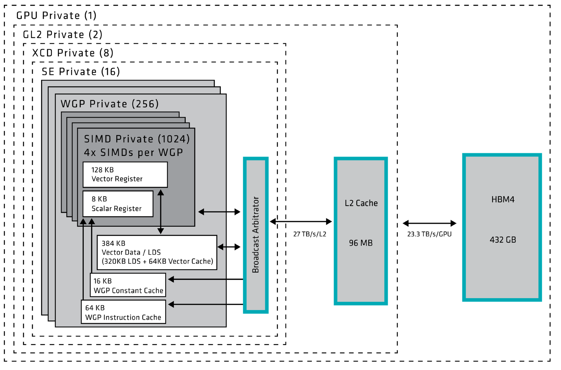
The inter-WGP caches have also changed to support this new design. Both the L1 Data Cache and the LDS have doubled in size to 64 KB of L1 Data Cache and 320 KB. The bandwidth of these caches has also doubled and can now do 2 256 bytes per clock.
Each XCD has 32 WGPs active, 34 physical WGPs of which 2 are fused off, which are broken up into 2 Shader Engines (SE) per XCD each with 16 WGPs. A shader engine is paired with a “Broadcast Arbitrator” replacing the L1 buffer (GL1) from RDNA4, which is now at the SE-level instead of the lower shader array-level. It works both as a write-combine buffer along with providing “up to 4x” bandwidth amplification by presumably broadcasting data.
The memory subsystem now allows multicast loads, accelerating matrix multiplication significantly by reducing redundant memory traffic. Imagine a GEMM that calculates C=A×B, then normally we would have each wavefront individually load a tile of, for example the A operand into the LDS of each WGP. With multicast loads we can instead load this tile of A into all relevant WGPs with a single multicast load instruction.
Each wavefront still loads a different B tile, but MI455X can fetch the common A data from L2 once and use the Broadcast Arbitrator to replicate it into all relevant WGPs private LDS allocations.
AMD calls this up to 4x bandwidth amplification, though the amplification happens after L2 and it does not quadruple L2 or HBM bandwidth. Instead, one unit of L2 traffic becomes four units of locally delivered data, reducing redundant cache reads and chiplet-link traffic while leaving each WGP with a nearby copy of the data.
SoC/Cache Changes
Moving down to the base dies, MI455X has 192 MB of Global L2 cache split across two Fabric Cache Dies (FCDs). Each FCD contains 96 1 MB SRAM blocks, giving it 96 MB of L2 capacity for the 128 WGPs attached to that cache domain. Each FCD can deliver up to 27 TB/s of L2 bandwidth, for an aggregate of 54 TB/s across the package.
This arrangement also changes how the cache domains behave. On CDNA 3 and CDNA 4, CUs attached to one base die could access the cache on another base die within the same package. CDNA 5 removes that capability: a WGP attached to one FCD cannot access the L2 cache on the other FCD. In that respect, MI455X behaves more like an AMD EPYC CPU, where a core on one CCD cannot directly access the cache attached to another CCD.
AMD made this change to improve the behavior of atomic operations across XCDs, eliminate the kernel flush boundary that MI300-series XCDs required for global visibility, and increase L2 data reuse. Although the two L2 domains are isolated from each other, each 96 MB cache can hold data associated with any global address in the GPU. That allows a WGP’s local L2 domain to cache data that might otherwise require traffic across the die-to-die interface.
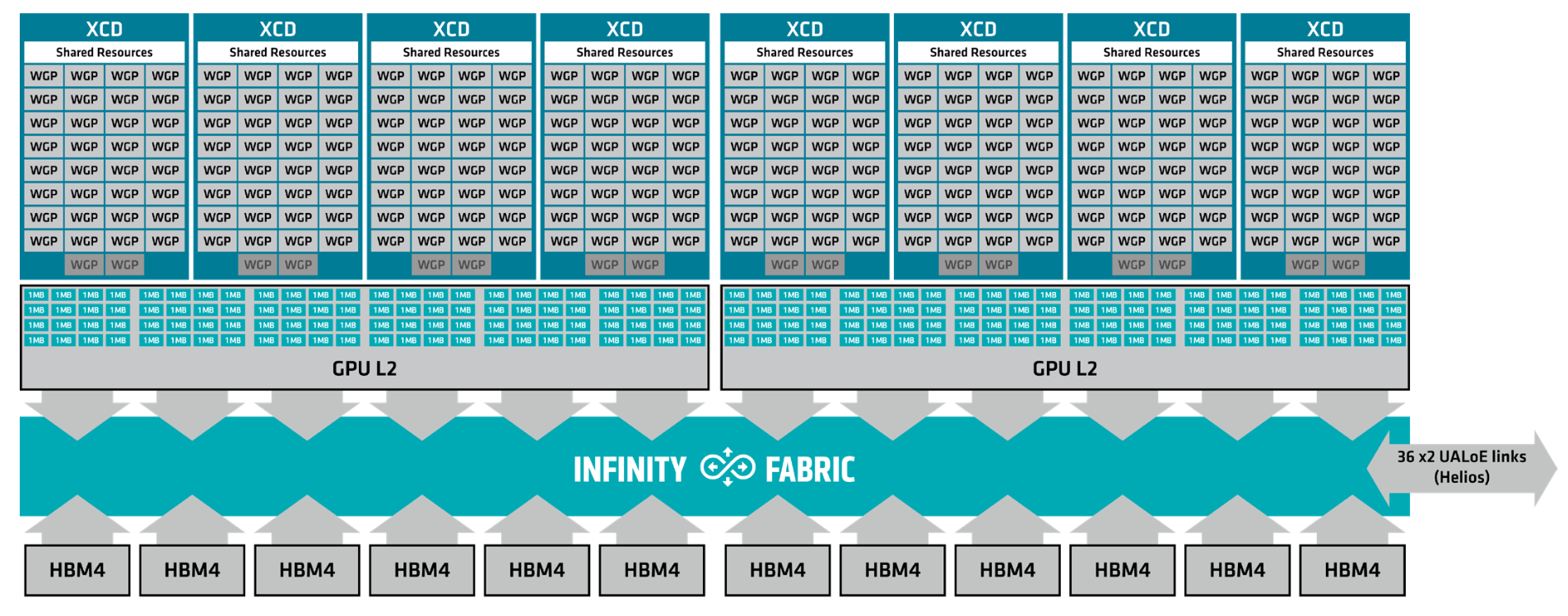
Speaking of that interface, the two FCDs are connected by a die-to-die interconnect providing approximately 14 TB/s of bidirectional bandwidth. The FCDs are also connected to 12 stacks of HBM4, with each stack providing 36 GB of capacity over a 2,048-bit interface. At approximately 7.6 GT/s per pin, those stacks provide a combined 432 GB of HBM4 and 23.3 TB/s of memory bandwidth.
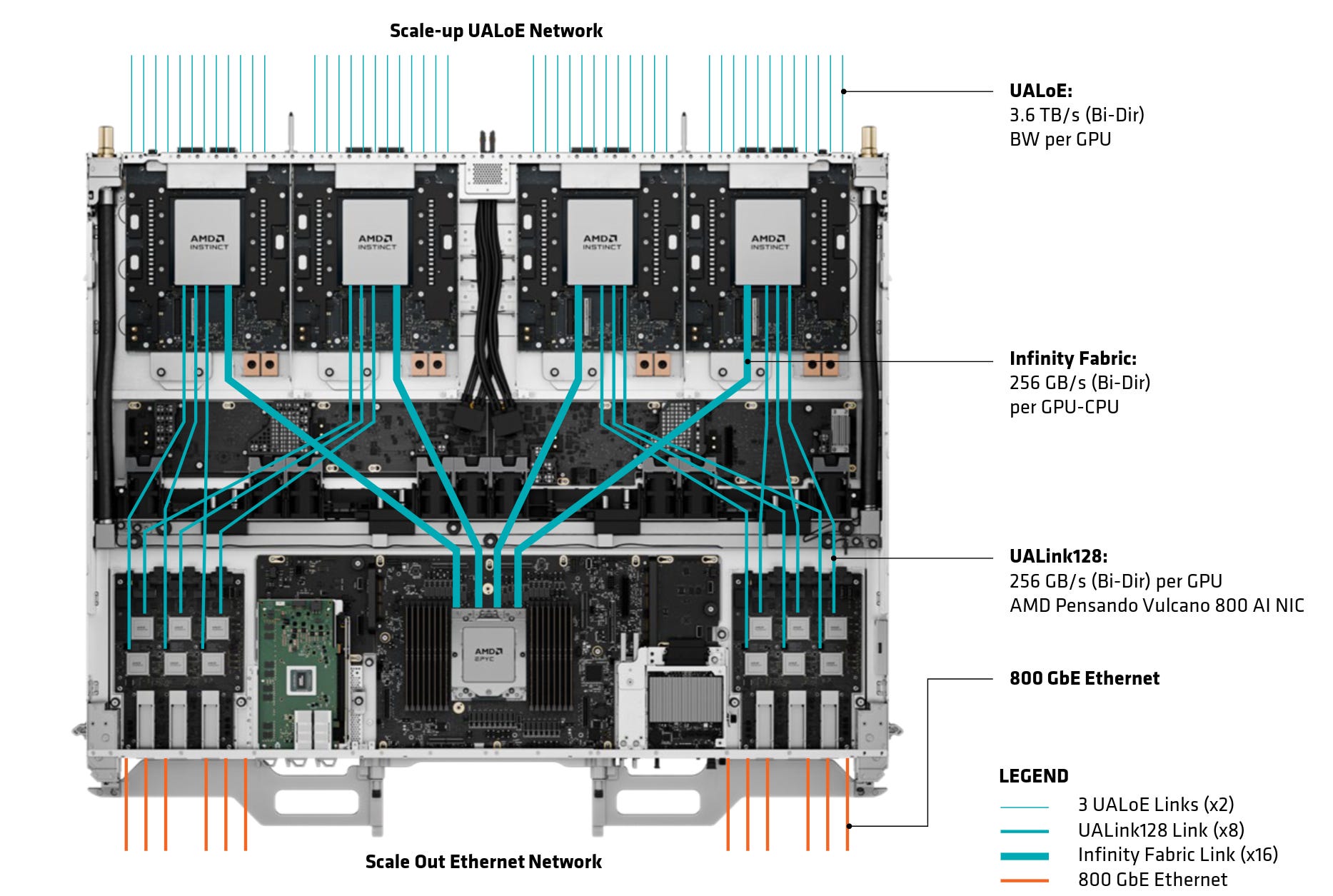
For any I/O that is external to a MI455X package, each FCD is attached to a IO die which does the very important job of connecting the GPU package to the host CPU, the scale-up network, and to the scale-out NICs. The CPU to GPU link that was previously serviced by PCIe has been replaced by a dedicated 16 lane AMD Infinity Fabric providing 256GB/s of bi-directional bandwidth which allows a coherent link between the GPU package and the host CPU.
Networking and AMD Helios Rackscale
Speaking of scaling up, along with the MI455X accelerator AMD is launching a validated rackscale platform for large scale AI infrastructure deployment. This is enabled by an increase in scale-up interfaces with MI455X having 36 x 400Gbit/s UALoE interfaces that implement 2 x 200G ethernet lanes each, comprising 3.6 TB/s of peak bidirectional bandwidth per GPU.
MI455X also introduces a split DMA architecture, which automatically associates traffic with the optimal link that reduces the topology awareness required for communication.
Helios uses OCP’s new Open Rack Wide form factor, compromising a cabinet 1.2m wide and 1.3m deep that provides. GPU’s are arranged in two groups of nine Compute Trays, each 1 OU in height. Each tray has four MI455X’s and one 96 core EPYC 9006 SP7. Each CPU is paired with 16 x 64GB DIMMS (for a total of 1TB of memory) and five E1.S slots for SSD’s. Six Helios Switch Trays provide a total of 12 switches connected directly via 3 UALoE links per GPU. Each switch provides 432 links at 200Gb/s, for an aggregate of 21.6TB/s per switch. This amounts to a scale-up bandwidth of 260TB/s bidirectionally.
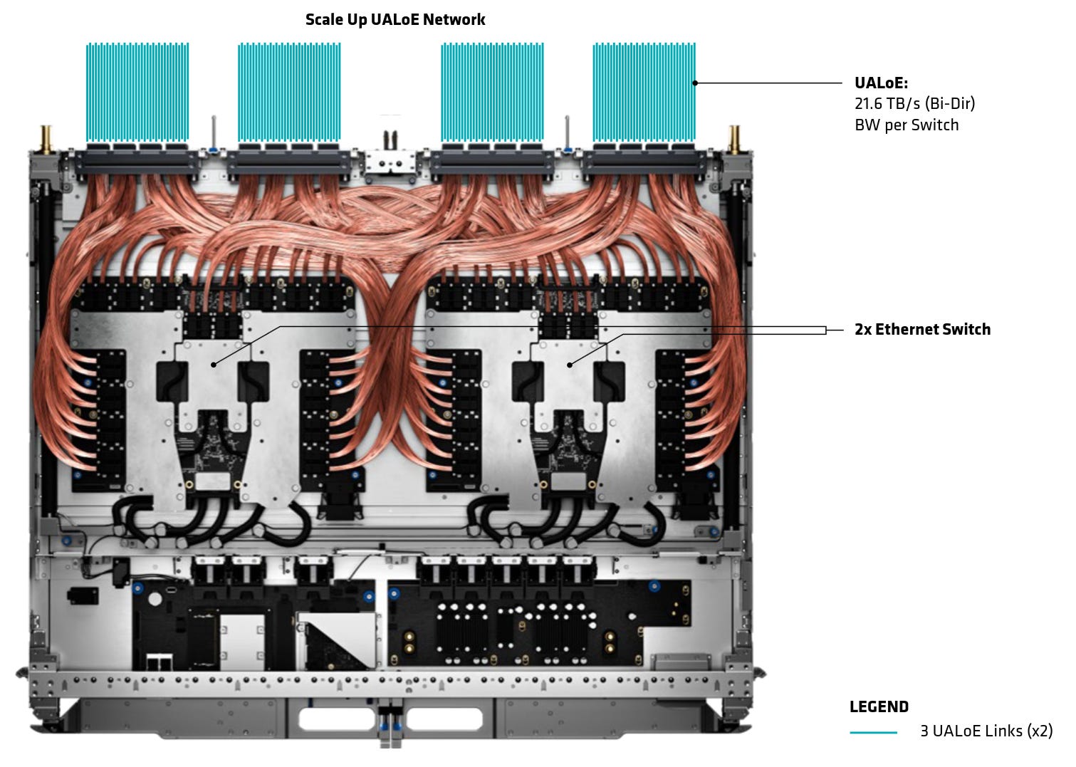
Scale-out is provided via two boards that can contain either 4 or 6 Pensando NICs, depending on how much scale-out the end customer would like, providing up to 43TB/s of backend bandwidth. With 72 GPUs in one rack, a Helios deployment is able to provide up to 2.9 EF at MXFP4 or 22.6 PF at FP32, alongside 31TB of shared HBM4 at a combined 1.7PB/s of memory bandwidth.
Conclusion: The King is Dead, Long Live the King
The basic GCN microarchitecture underpinned every single one of AMD’s compute accelerators for nearly 15 years starting with Tahiti, followed by Fiji, Vega, and the first 4 generations of CDNA. With CDNA5 AMD has moved over to a microarchitecture that is based on the RDNA series putting a bookend to the long-lived line that was the GCN microarchitecture.
And with that bookend comes the start of a new story for AMD’s Datacenter Accelerators, one that now isn’t just about a single GPU but scaling to 72 GPUs in a rack along with scaling the number of racks. For that AMD is relying on nearly every part of their business from EPYC Server CPUs, to Pensando Networking, to the base GFX12 from the Radeon Division, to combine all of them into the AMD Helios Rack.
 |
|
No Zen 6 details?