AMD acquired ATI in 2006, hoping ATI's GPU expertise would combine with AMD's CPU know-how to create integrated solutions worth more than the sum of their parts. AMD uses the name "Accelerated Processing Unit" (APU) to refer to chips with integrated graphics. APUs have come a long way from their beginnings in 2011's Llano. Modern APUs like Van Gogh, Phoenix, and Strix Point make AMD a powerful competitor in the mobile PC gaming market.
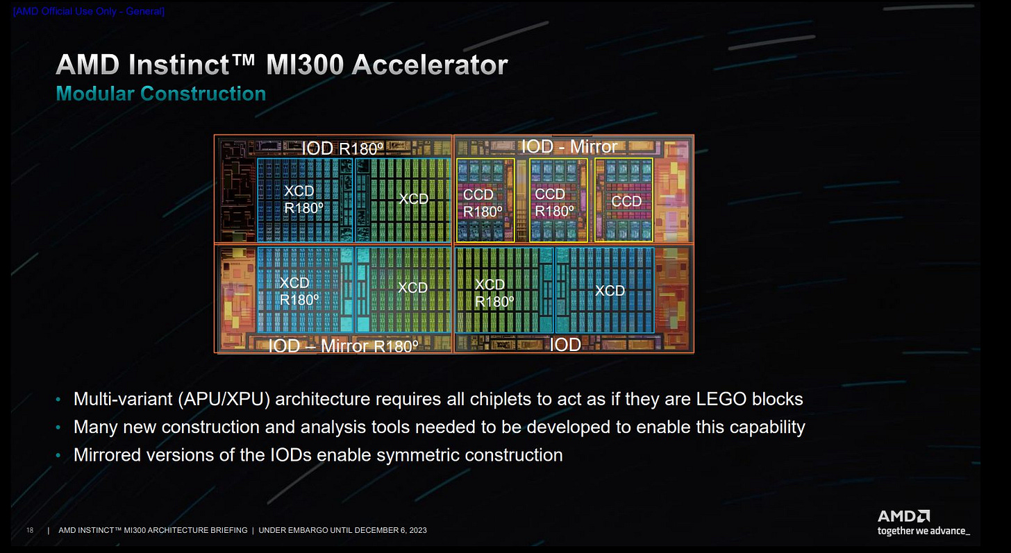
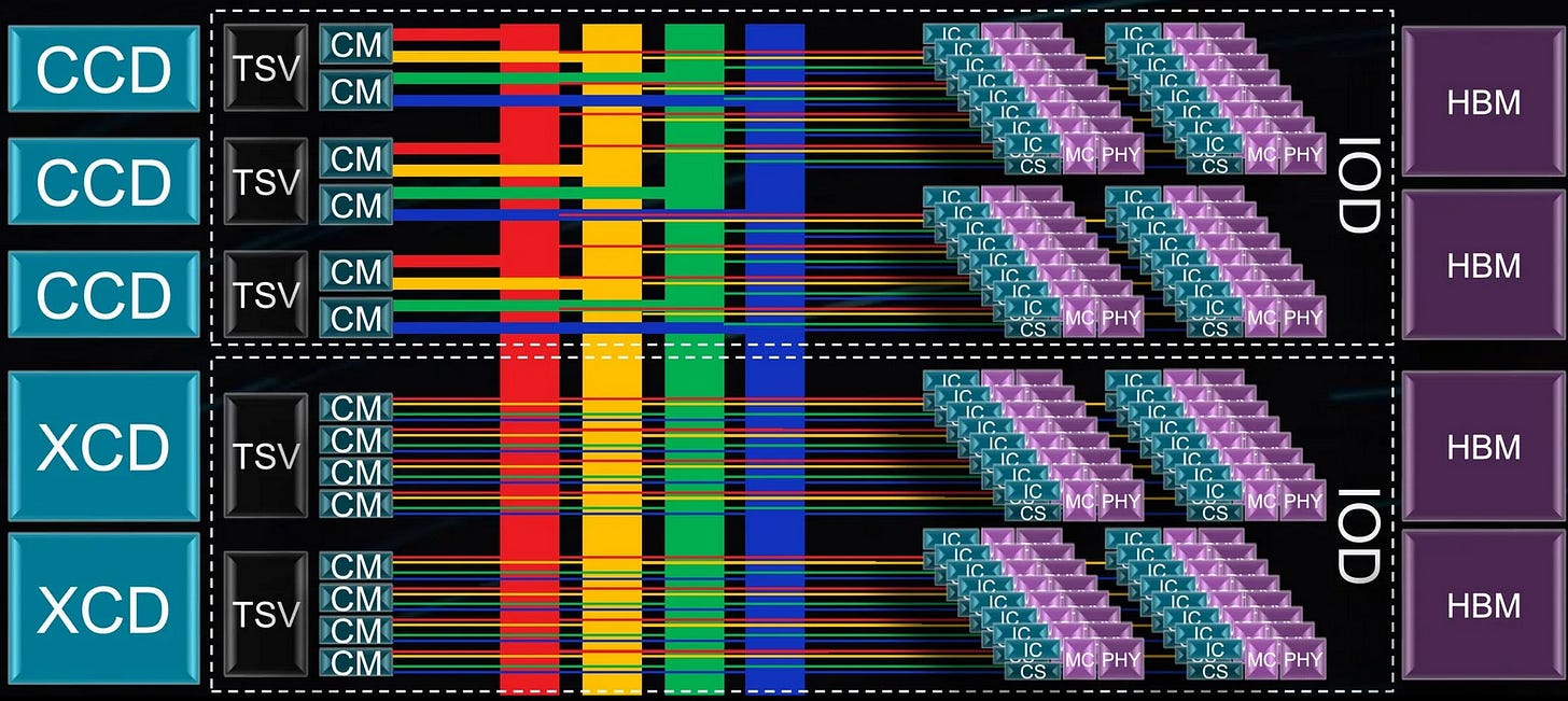
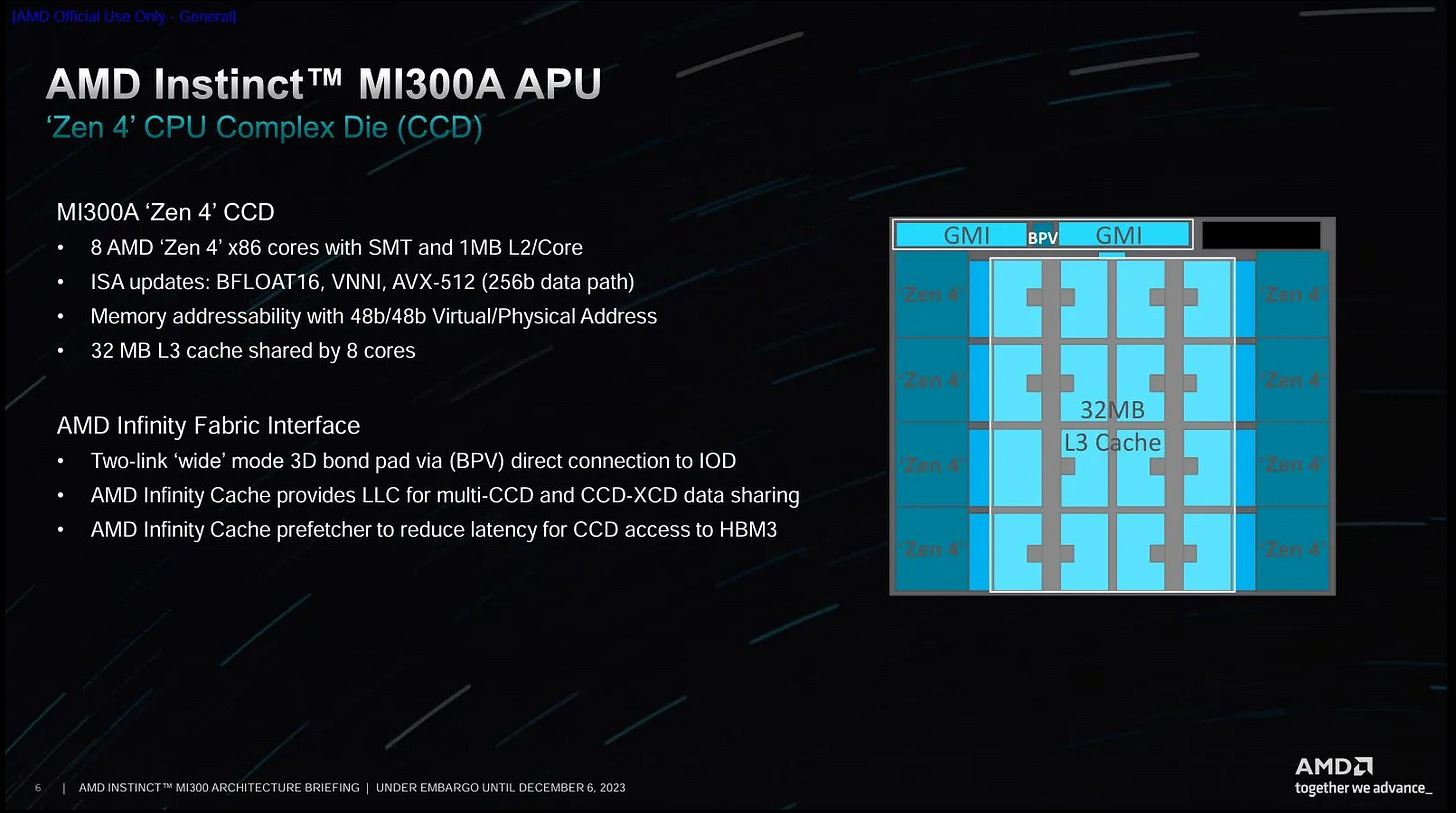
But AMD’s ambitions go further. The company wants to push integrated graphics into the high performance compute and AI space. iGPUs have advantages like not needing a separate CPU chip to drive the system, and sharing a pool of memory across both the CPU and GPU. To make those advantages meaningful, AMD has to build an APU large enough to rival other high performance compute solutions. To that end, MI300A uses a monstrous chiplet configuration. Three Core Complex Dies (CCDs) each contain eight Zen 4 cores. Six Accelerator Complex Dies (XCDs) each contain 38 CDNA3 Compute Units. All of that compute sits on top of four IO dies (IODs), which act as an active interposer with cache. The IODs then sit on an active interposer that enables fast cross-IOD communication and access to HBM3 memory.
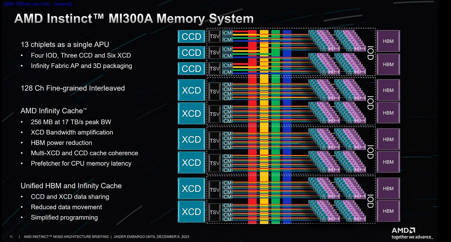
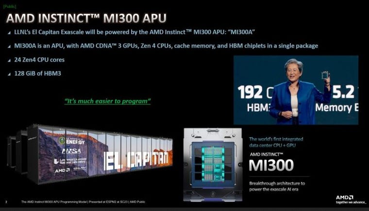
Basically, the Instinct MI300A is a MI300X that trades some GPU power for 24 Zen 4 cores running at 3.7 GHz. Both MI300 variants have a similar memory subsystem, with 256 MB of memory side cache (Infinity Cache), and 5.3 TB/s of HBM3 bandwidth. Chips and Cheese has already covered MI300X and AMD’s CDNA3 compute GPU architecture in another article. Also, AMD has said MI300A’s CCDs are adapted from regular Zen 4 CCDs, and we’ve covered Zen 4 in a series of other articles. Therefore, I’ll focus on MI300A’s massive Infinity Fabric implementation in this article.
Acknowledgments
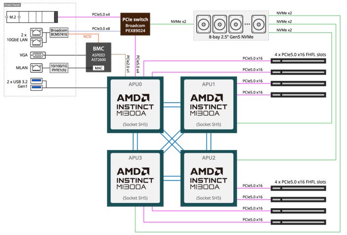
Special thanks goes out to AMD and GIGABYTE along with their Launchpad service, who generously let Chips and Cheese play around with a massive quad-socket MI300A system in the form of the G383-R80-AAP1 for over 2 weeks. As always, our testing was our own.
Infinity Fabric on a Giant APU
AMD built MI300A on top of their Infinity Fabric interconnect, which consists of many networked components that work together to enable coherent memory access. With 24 CPU cores and 228 GPU compute units, MI300A is a very large system and is supported by a giant Infinity Fabric network.
Infinity Fabric has CPU and GPU dies talk to Coherent Master (CM) blocks, which abstract out the rest of Infinity Fabric from that compute block’s perspective. The CM has a memory map, and sends packets (flits) addressed to whichever agent is responsible for the requested memory address. Then, a network of buses, switches, and off-die interfaces ensure the flit reaches its destination.
Most CPU and GPU requests go to physical addresses backed by DRAM. Coherent Slaves (CS) handle those addresses, and are responsible for ensuring requests are satisfied with the most up-to-date data. To carry this out, the CS has a probe filter, and is attached to a memory controller.
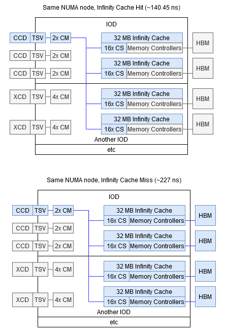
In MI300A, the CS is also co-located with a 2 MB Infinity Fabric block. Thus the CS can satisfy a request from several locations:
Its 2 MB Infinity Cache slice, if the requested address hits in cache
Its attached memory controller, on a cache miss
By sending a probe to another CM, if the CS’s probe filter indicates the requested line is cached in modified state on any CPU or GPU die
All this means CPU and GPU blocks can be confident they’ll get the most up-to-date data without doing anything special. Of course, how fast they get their data is another question. All of those data sources have very high latency compared to a desktop Zen 4 system.
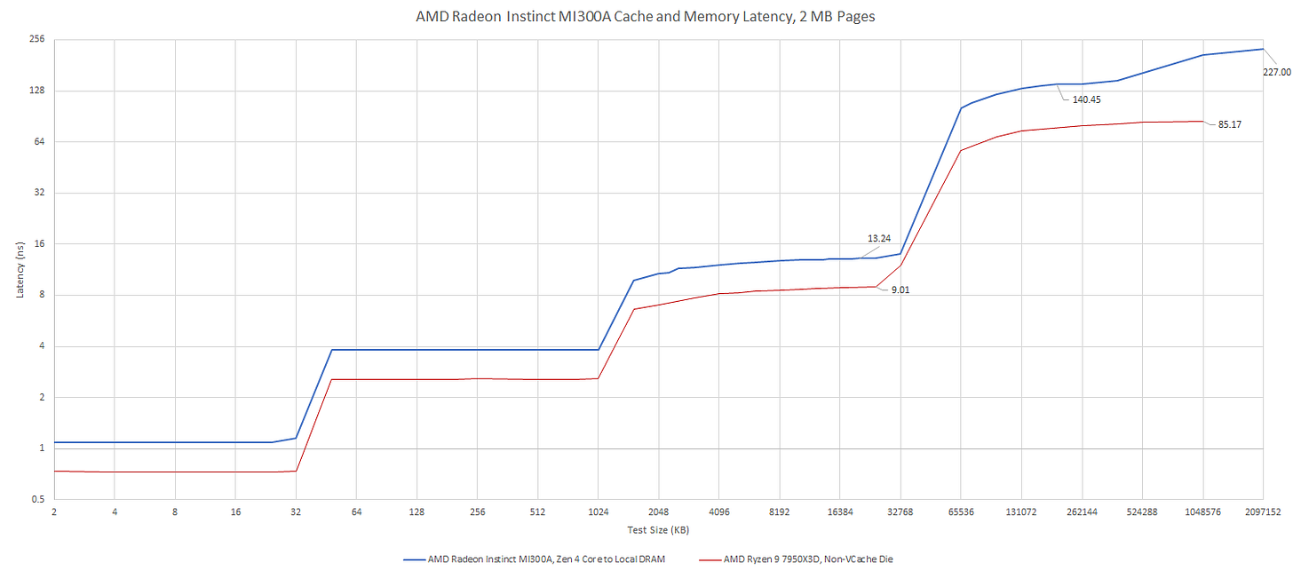
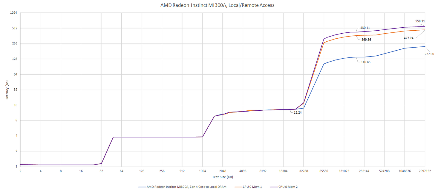
An Infinity Cache hit has a load-to-use latency of over 140 ns. Even DRAM on the AMD Ryzen 9 7950X3D shows less latency. Missing Infinity Cache of course drives latency up even higher, to a staggering 227 ns. HBM stands for High Bandwidth Memory, not low latency memory, and it shows. High Infinity Cache hit latency also suggests a lot of latency comes from traversing a giant Infinity Fabric network.
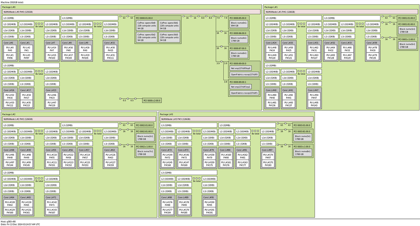
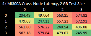
Things only go up from here, meaning latency gets worse. Infinity Fabric’s transport layer extends beyond MI300A’s chip boundary, supporting multi-socket NUMA configurations. The test system generously provided by AMD and Gigabyte comes with four MI300A chips, each of which is exposed as a NUMA node. Cross-node DRAM accesses carry a hefty latency penalty.
numactl --hardware shows equal distance between all nodes. Gigabyte’s documentation suggests each MI300A chip is directly connected to all of its peers. However, pairs of MI300A chips enjoy lower latency access to each other’s memory pools.
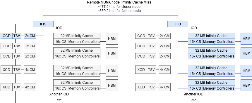
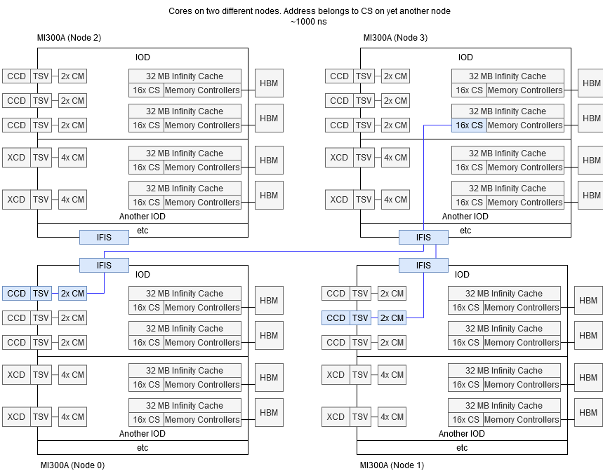
Remote DRAM latency is around 477 ns to a closer node, and 559 ns to a far one. I suspect the latency difference is related to where the cross-socket link is located relative to the CPU cores. Getting to a cross-socket link located on a different IO die probably adds a measurable amount of latency.
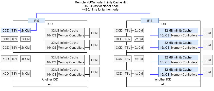
Infinity Cache can reduce remote access latency to about 369 and 430 ns for close and far nodes respectively. Those latencies are still high because a MI300A chip’s Infinity Cache can’t cache addresses belonging to other nodes. Because Infinity Cache is a memory side cache attached to CS-es, each Infinity Cache slice can only cache addresses owned by that CS. That in turn means each Infinity Cache slice can only handle addresses backed by that CS’s memory controller.
Thus AMD’s Infinity Cache implementation sacrifices some NUMA performance to keep things simple. Tying Infinity Cache blocks to the CS-es lets MI300A’s large 256 MB memory-side cache seamlessly slot into the Infinity Fabric subsystem. Doing so should keep extra coherency management hardware to a minimum, with only a bit of extra complexity at the CS. A decoupled layer of cache could potentially insulate cores from cross-node DRAM access latency, but would create another set of cache controllers that have to perform both the role of a CM and CS. For a project as ambitious as MI300A, I can respect the decision to keep things simple.
Compared to a conventional dual socket server system, MI300A has very high DRAM access latency. That applies for accesses to both directly attached and remote DRAM, and means MI300A’s Zen 4 cores could struggle a bit compared to other Zen 4 implementations.
Infinity Cache and DRAM may be the most common data sources. A CS may have to satisfy a memory request by sending a probe, if its probe filter indicates the requested address has been modified elsewhere in the system. Such requests only account for a tiny minority of memory traffic, but are important for making sure all CPU and GPU cores get a consistent view of memory.

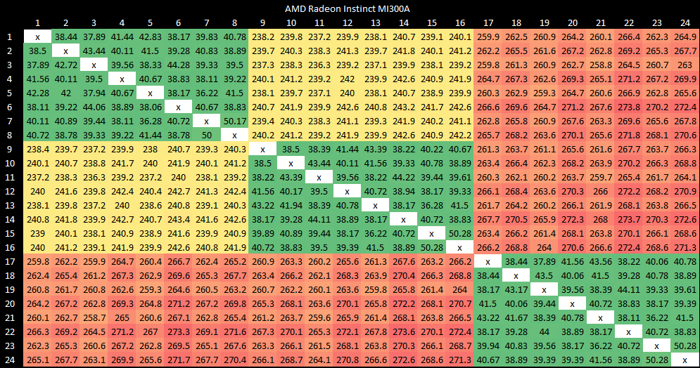
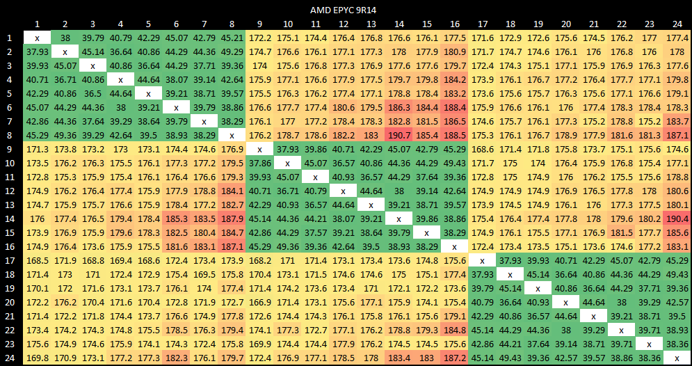
Cross-CCD transfers within a MI300A chip have 260-450 ns of latency, likely depending on which CS the tested address is homed to. It’s high compared to an EPYC system, but MI300A does have a much larger Infinity Fabric network.
A large Infinity Fabric network gets absolutely monstrous with a party of four MI300A chips. Results from a core-to-core latency test show very high latency across node boundaries. Worst case latencies show up when the responsible CS is on a different node than the requesting cores. A core to core transfer in that case can involve three MI300A chips – two with cores being tested, and a third to orchestrate the transfer.
That sort of high latency shows the challenge of creating a hypothetical quad-socket EPYC system. AMD chose to boost core count within a socket rather than scale beyond two sockets as they’ve done in the past. Core to core latency on a quad socket MI300A system helps explain why. Looking at one socket gives a better picture.
Still, core to core transfers are very rare in practice. I consider core to core latency test results to be just about irrelevant to application performance. I’m only showing test results here to explain the system topology.
Infinity Fabric Bandwidth
The Instinct MI300A’s memory subsystem may not be kind to its Zen 4 cores from a latency perspective. From the bandwidth side though, it’s an all-you-can-eat buffet where Infinity Fabric links between each CCD and the rest of the system is your plate. These are big plates too. Each octa-core Zen 4 CCD has a GMI-wide configuration with two 32B/cycle links in both directions.
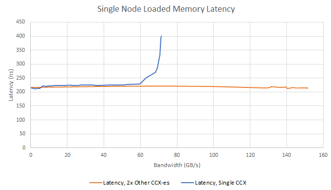
Wider Infinity Fabric links are critical because they let AMD run MI300A’s massive Infinity Fabric network at a lower clock. They also help the Zen 4 cores get access to more memory bandwidth than their desktop counterparts. Previously I looked at pinch points in AMD’s Infinity Fabric on a Zen 4 desktop system. With regards to pinch points, MI300A’s Zen 4 CCDs show similar behavior to desktop Zen 4, where bandwidth hungry threads can cause noisy neighbor effects for a latency sensitive thread running on the same CCD. 71 GB/s is higher than the 64 GB/s of read bandwidth that a desktop Zen 4 CCD can get with a 2 GHz Infinity Fabric clock. But once you get to that bandwidth limit, latency starts to go up. Similarly, a latency sensitive thread running on one CCD is insulated against bandwidth hungry code running on other CCDs.
Unlike desktop Zen 4, hitting Infinity Fabric or DRAM bandwidth limits with the CPU cores is simply impossible. Even with the two other CCDs pulling north of 140 GB/s, latency from the first CCD is unaffected. On the other hand, the MI300A’s three CCDs can only consume a fraction of the chip’s HBM3 bandwidth.
That 5.3 TB/s of DRAM bandwidth is really there to feed the GPU dies, not the CPU. MI300A isn’t unique in not letting the CPUs get full access to DRAM bandwidth. Apple’s M1 Max similarly can’t feed its CPU cores with the chip’s full LPDDR5 bandwidth, likely due to pinch points between the CPU core clusters and the rest of the system.
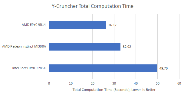
MI300A’s 24 Zen 4 cores achieve 212 GB/s of read bandwidth, and 314 GB/s if I use a read-modify-write pattern that exercises the CPU die Infinity Fabric links in both directions. While that’s not enough to make the memory controllers sweat, it’s a ton of bandwidth on a per-core basis. Unfortunately, latency is more important for CPU workloads. MI300A’s Zen 4 cores fall behind their equally clocked counterparts sitting on top of a server memory subsystem, even when running a bandwidth intensive workload like Y-Cruncher.
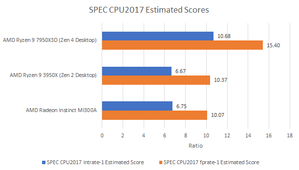
SPEC CPU2017 provides a glimpse at how MI300A Zen 4 core might stack up in a variety of general purpose workloads. Against a Zen 4 desktop system, there’s no comparison. MI300A’s single threaded integer performance is about on the same level as the Zen 2 based Ryzen 9 3950X. In my opinion, that’s actually a very good place to be. The 3950X was a top-notch processor a few years ago, and its single threaded performance is still decent in absolute terms.
Cross-Node Bandwidth
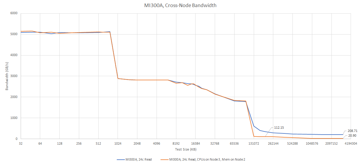
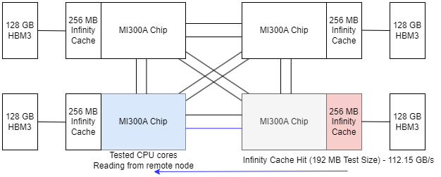
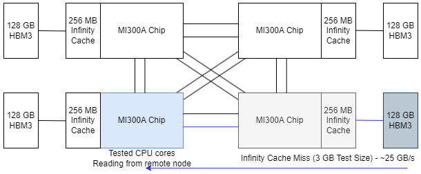
Reading from memory attached to other MI300A chips is slower, because traffic must flow through off-socket Infinity Fabric links. These cross-socket links provide 128 GB/s of bandwidth in each direction, and I can get quite close with test sizes that fit within Infinity Cache capacity.
Larger test sizes however see very low cross-socket bandwidth compared to conventional dual socket server setups. I tried a few test modifications, like having all test threads terminate when a flag is set rather than accessing a fixed amount of data, or using 2 MB pages to reduce overhead from address translation.
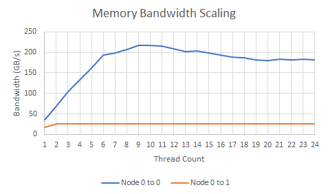
Neither of those made a significant difference, and I couldn’t read from a remote node’s DRAM at more than 25-26 GB/s.
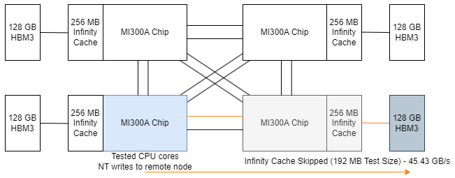
I also tried using different access patterns. Writes do achieve higher bandwidth, likely because they’re not latency limited. Specifically, I’m using non-temporal writes because regular writes typically require read-for-ownership (RFO) requests, which would run into read latency. Otherwise, the memory subsystem would risk torn writes. Some CPUs like Intel’s Ice Lake server chips can avoid RFOs in certain situations, but I’m using non-temporal writes so that I know exactly what I’m dealing with.
Non-temporal writes appear to skip Infinity Cache. 45.43 GB/s is better than 25 GB/s, but still well short of the 112 GB/s that the cross-socket links are clearly capable of achieving. I also tried using different thread counts to see if I was being latency limited.
Bandwidth doesn’t scale once I load more than two cores, suggesting the amount of memory level parallelism achievable from a core isn’t a limiting factor. I still suspect I’m latency limited at some point, because writes do show increased bandwidth and the cross-socket links are capable of hitting 112 GB/s when fetching data from another socket’s Infinity Cache. But I’m not sure where the bottleneck may be.
CPU to GPU Communication
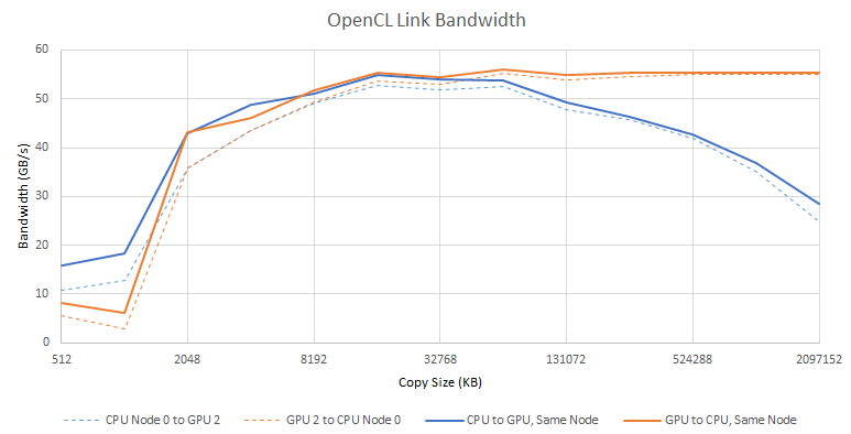
Integrated GPU setups like the one in AMD’s Instinct MI300A can offer easier CPU to GPU communication, because both use the same pool of main memory. The most basic and portable way of using GPU acceleration involves explicitly copying data between CPU and GPU memory spaces. Here, I’m testing OpenCL’s clEnqueueWriteBuffer and clEnqueueReadBuffer functions, which copy data to and from GPU memory respectively.
These functions often use the GPU’s DMA engines, which are less sensitive to latency than CPU cores. MI300A can achieve a good 55.9 GB/s, even when copying data to another MI300A chip. That’s more bandwidth than I could achieve with cross-node CPU-side requests, and is another suggestion that my cross-node CPU tests were latency bound. Small copy sizes can still be affected by latency, especially when moving data between different MI300A chips. This likely has to do with startup latency for the DMA engines too.
Shared Virtual Memory
Newer GPUs can avoid explicitly copying data between CPU and GPU memory. This “zero copy” behavior may be more natural to implement on an integrated GPU like MI300A. However, some modern discrete GPUs can also support zero-copy behavior.
I’m testing this via OpenCL’s Shared Virtual Memory (SVM) feature. SVM lets programmers use the same memory pointers for both the CPU and GPU. However, SVM by itself doesn’t mandate zero-copy behavior. SVM further defines different levels of support that define how much explicit synchronization the programmer needs to do in order to make writes visible across CPU/GPU boundaries.
Coarse grained buffer sharing: This is SVM’s baseline behavior. You have to unmap the buffer from CPU memory space via
clEnqueueSVMUnmapbefore CPU-side writes are made visible to the GPU. Similarly, you have to callclEnqueueSVMMapto map the buffer into CPU memory before results generated on the GPU can be seen by the CPU.Fine grained buffer sharing: Visibility is guaranteed after a GPU kernel (program) finishes executing, and CPU-side writes made before a GPU kernel starts running are visible on the GPU.
Atomics: Code running on the CPU and GPU can exchange data “live” without intervention from the GPU driver. GPU code can almost be treated like extra CPU threads, from the perspective of cross-thread communication.
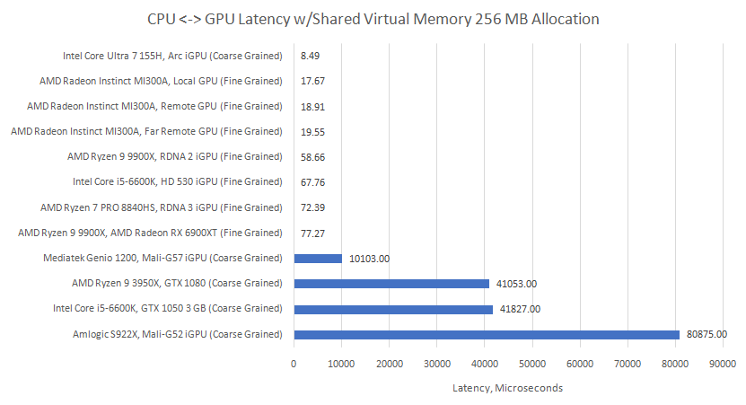
SVM doesn’t guarantee zero copy behavior, because GPU drivers can implement SVM by doing a memory copy under the hood. Therefore, I’m testing for zero copy behavior by allocating a 256 MB buffer and only changing a single 32-bit value in it. If the GPU has zero copy support, I’ll see that change propagated across CPU/GPU boundaries with very little latency. But if the GPU drivers decide to copy the entire 256 MB buffer, latency will be much higher.
All GPUs I’ve tested with fine grained buffer sharing support appear to exhibit zero-copy behavior. Some GPUs with only coarse grained buffer sharing support zero copy too. Intel’s Core Ultra 7 155H (Meteor Lake) iGPU only supports coarse grained buffer sharing, but clearly avoids copying entire buffers and is actually the fastest one here. Nvidia discrete GPUs meanwhile fly into the millisecond timescale. It’s is an indication that Nvidia’s Pascal GPUs lack strong hardware cache coherency support, forcing the GPU drivers to copy the entire 256 MB buffer rather than transferring the single modified cacheline. Similarly, two ARM Mali iGPUs appear unable to support zero copy behavior. The Mediatek Genio 1200 does benefit from avoiding copies over a PCIe bus, but it’s still orders of magnitude off zero copy latency.
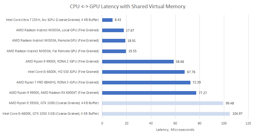
Switching over to 4 KB allocations further suggests much of the microsecond scale latency comes from synchronization overhead. The two discrete Nvidia GPUs I tested aren’t far off when they have to copy very little data. Now that GPUs without zero copy support aren’t ruining the graph scale for everyone else, it’s clear MI300A can support zero copy behavior and does quite well. Synchronization overhead is lower than any other system I tested besides Intel’s Meteor Lake. Even when CPU cores on one MI300A chip need to synchronize with another MI300A chip’s GPU, latency only goes up a little bit and remains excellent overall.
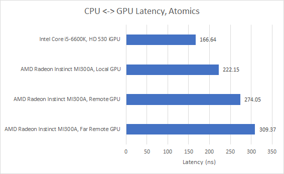
Atomics provide a way to get around that synchronization overhead. They let writes become visible across CPU/GPU boundaries without waiting for a GPU kernel to finish and for the GPU driver to do all the necessary maintenance around that. AMD’s MI300A does not advertise atomics support. However, it works well enough for me to adapt my core to core latency test to run with one GPU-side thread and one CPU-side thread. The GPU kernel uses OpenCL’s atomic_cmpxchg, while the CPU thread uses _InterlockedCompareExchange on Windows/MSVC or __sync_bool_compare_and_swap on Linux/GCC.
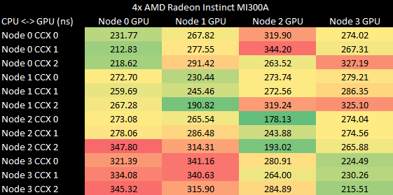
With GPU drivers and higher level synchronization out of the picture, results are back in nanosecond territory. Bouncing values between the CPU and GPU is somewhat slower on the MI300A than on Intel’s Core i5-6600K, which does advertise atomics support. Still, 222.15 ns is excellent when ensuring coherency across a chip as large as the MI300A, and is similar to latency between the Zen 4 CCDs. More impressively, CPU to GPU latency remains well under control even when a CPU thread is talking to a different MI300A chip’s GPU.
MI300A appears to do an excellent job of managing cache coherency between CPUs and GPUs, at least from this basic test. Worst case latency is far better than in the core to core latency test. Part of this could come down to how GPUs handle writes and atomics. CPUs have write-back L1 caches, and execute atomics by taking ownership of the cacheline to ensure no one else touches it during the atomic operation. GPUs have write-through or read-only L1 caches, so writes go directly to L2. Atomic operations get handled by dedicated execution units at the L2 cache, rather than at the Compute Units (CUs). I suspect that lowers latency for contended atomics because there’s no need to probe CU-private caches. AMD may also have put a lot of effort into optimizing GPU-side atomics. After all, MI300A’s GPU power is front and center in the design.
Final Words
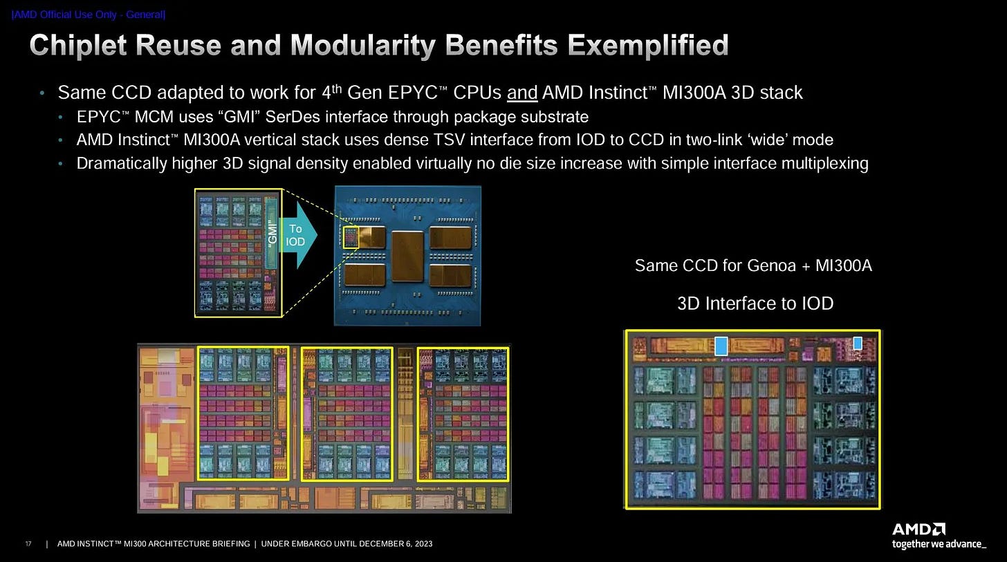
The Instinct MI300A combines AMD’s CPU and GPU prowess on a massive scale. At the physical level, it’s a showcase of AMD’s willingness to use advanced packaging techniques and go big with them. MI300’s IO dies can connect to either XCDs or CCDs, letting AMD create two products with a lot of die reuse and thus streamlined manufacturing logistics.
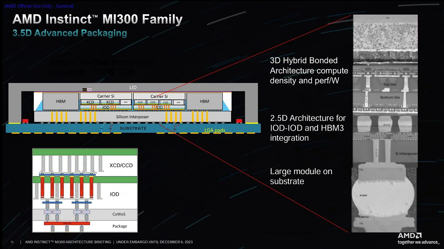
A grab bag of advanced packaging technologies make it all possible. MI300A is built from dies stacked on top of dies, which are in turn stacked on top of another die. TSVs between vertically stacked dies provide massive bandwidth. IO dies have plenty of bandwidth to their adjacent partners too.
Each IOD utilizes nearly the full “beachfront” die edge to implement these interfaces. Because each IOD is nearly abutting its adjacent neighbors, we were able to leverage a highly optimized “ultra short reach” (USR) SerDes PHY previously developed for our Radeon GPUs
AMD Instinct MI300X Accelerator: Packaging and Architecture Co-Optimization
This high cross-die bandwidth lets MI300X present the programmer with a huge unified GPU. AMD’s prior MI250X and Intel’s Ponte Vecchio didn’t have enough bandwidth between two halves of the chip, and had to be handled as two separate GPUs. By integrating a CPU, MI300A can further simplify programming because CPU to GPU communication has low cost.
Physical design is only half the picture. Making more people work on one component can create a too many chefs in the kitchen problem. Splitting people into teams with well defined areas of responsibility can help. But teams still need to communicate, and getting everyone on the same page can be both time consuming and frustrating. Of course, I can’t tell what’s going on inside AMD with absolute confidence. But MI300A’s design hints at a lot of well defined interfaces between components.
AMD’s compute blocks interface with the system via Infinity Fabric, which acts as a giant abstraction layer. Once a CPU or GPU implements the Coherent Master’s interface, it can enjoy coherent memory access. Engineers working on a CPU core cluster (CCX) don’t have to care what happens beyond the Coherent Master. The chip in question could have DDR5, LPDDR5, or HBM3 memory. The system could have one other CPU cluster as in a Ryzen system, 11 other CPU clusters in an EPYC system, or 2 other CPU clusters and 6 GPU blocks. As long as the CCX adheres to the Coherent Master’s expectations, everything beyond is handled by a different team. The same applies to GPU blocks.
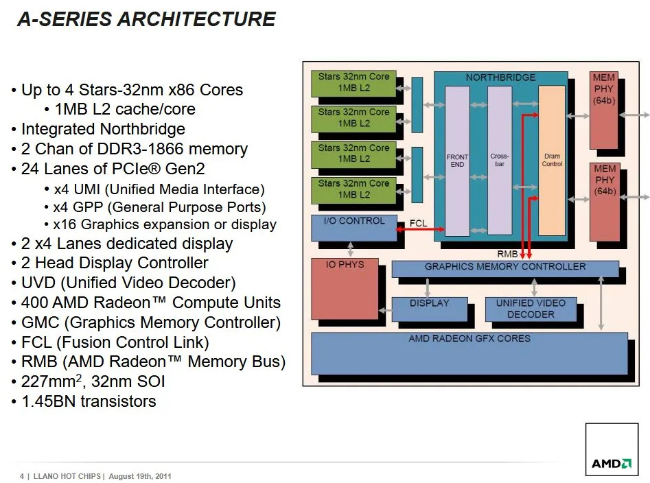
It’s a stark contrast to Llano, where the iGPU used custom links shoehorned into the CPU memory subsystem. Llano’s Terascale 2 iGPU had to make requests across different links depending on whether it needed coherent memory access, increasing design complexity and introducing funny bandwidth limitations for certain memory types. More importantly, engineers working on the GPU-side “Graphics Memory Controller” would likely need intimate knowledge of the Northbridge’s implementation details. Because an internal Northbridge change could break the Graphics Memory Controller’s expectations, engineers working on the Northbridge would either have to tiptoe their way around to maintain compatibility, or constantly go back and forth with the Graphics Memory Controller people to make sure everything still works after a change. AMD’s current model mitigates that inefficiency, and likely helps preserve engineer sanity.
Abstraction layers like Infinity Fabric give AMD the ability to pursue ambitious projects like MI300X and MI300. But that doesn’t mean building a big APU is easy. CPUs and GPUs favor different memory subsystem characteristics, so any design has to be a compromise. MI300A addresses those difficulties by shamelessly favoring the GPU. Infinity Cache and HBM3 make for a high latency, high bandwidth memory subsystem that’s excellent for a latency tolerant GPU, but not so hot for a latency sensitive CPU. MI300A’s Zen 4 cores can’t keep pace with their mainstream client or server counterparts. Everything get even harder when the cache coherency domain extends beyond chip boundaries. Cross-node memory accesses or coherency traffic have higher cost on a multi-socket MI300A system than on a typical dual socket server setup.
PC enthusiasts likely won’t accept the significant CPU-side compromises involved with designing a large iGPU solution, which is why large iGPUs have never taken off in the PC market. But for MI300A, that’s fine. Its CPU cores are meant to support its giant GPU, and not to provide high responsiveness across a wide range of general purpose applications. For that purpose, MI300A’s CPU side still packs a decent punch. 24 cores are nothing to sneeze at, especially when each can perform like the fastest clocking core on the Ryzen 9 3950X.
More importantly, the MI300A’s CPU cores are positioned to quickly share data with the GPU. That could provide an advantage if programmers have to do a bit of processing on the CPU side between long running GPU kernels. 24 Zen 4 cores per socket could be just enough CPU power to let programmers feed a MI300X-like GPU power without needing a separate host CPU.
AMD has already scored several major supercomputings win with this design with the biggest being LLNL's El Capitan using quad-socket MI300A nodes, and occupies the top spot in TOP500's November 2024 list. The company took a long road over many years to realize the dreams that started with Llano, and AMD's engineers have a lot to be proud of. I look forward to seeing what they bring up next.
And again, we'd like to give a massive shout out to GIGABYTE and their Launchpad service without whom this testing would not be possible without!
If you like the content then consider heading over to the Patreon or PayPal if you want to toss a few bucks to Chips and Cheese. Also consider joining the Discord.







Cross-node bandwidth pattern looks like your memory allocation is all in just one channel of one HBM per socket. Are there no options to stripe memory across all channels?
Do you think that there will be a MI355A?