Hot Chips 2024: Qualcomm’s Oryon Core
Today, Qualcomm is presenting on their Oryon core. We’ve covered this core previously in a separate article, so I’ll focus on new details or differences covered in the review.
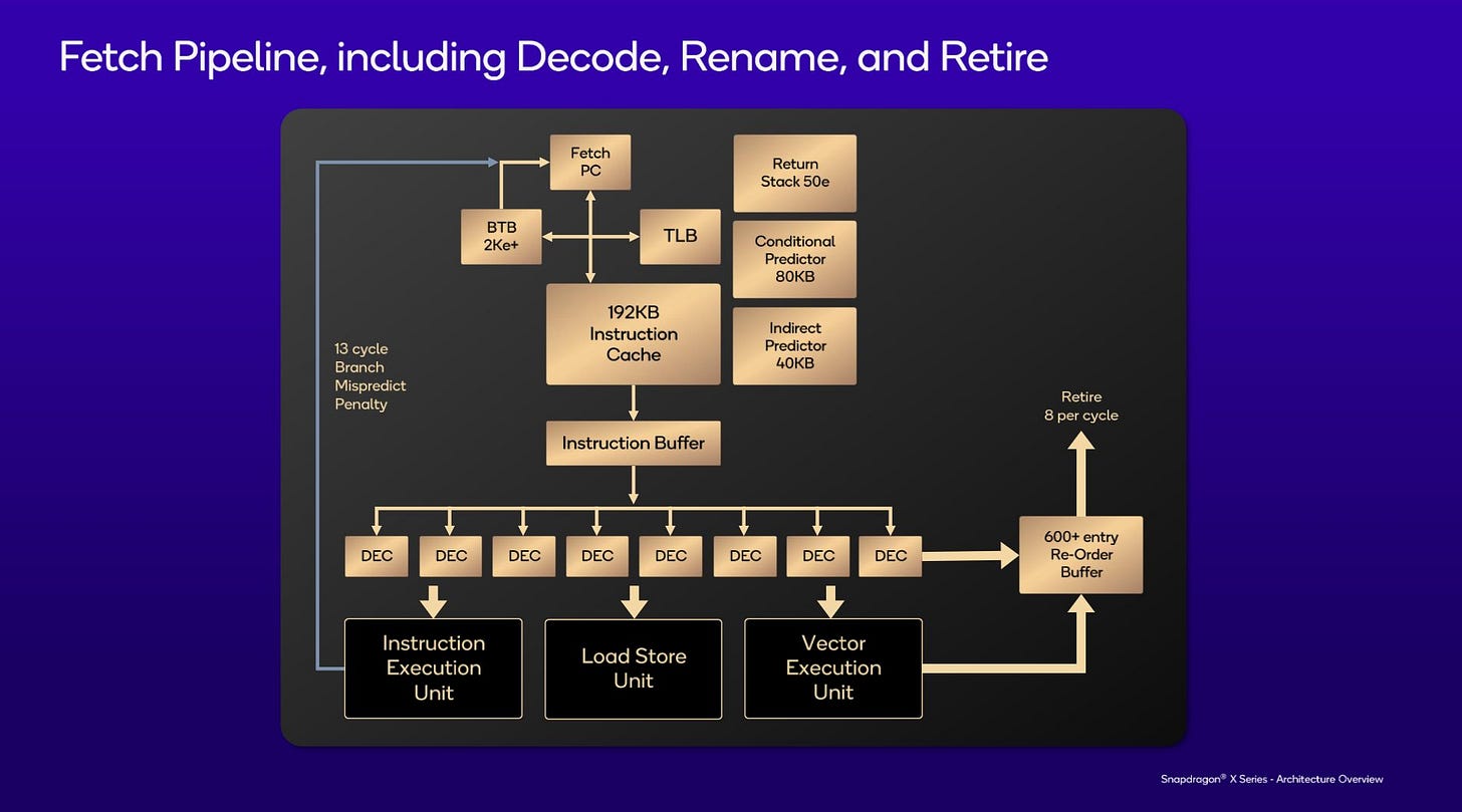
At the frontend, Oryon has substantial branch prediction resources to feed the 8-wide decoder. Qualcomm has disclosed that the branch predictor uses the TAGE (Tagged Geometric length) prediction method, which lets the predictor flexibly choose between different history lengths depending on what a branch needs. Additionally, slides detail the storage budget for the different predictors.
While a 80 KB storage budget for the conditional predictor sounds like a lot, and is nearly as much as the 96 KB L1 data cache, it’s not too out of line. From die shots, AMD also appears to allocate substantial storage to its branch predictor. The paper on L-TAGE uses a 64 KB storage budget, and 80 KB is not too much larger than that. Oryon’s uses a smaller prediction budget for indirect branches, but also uses global history and a similar prediction algorithm to select between targets.
Qualcomm noted that while their 13 cycle mispredict penalty is not industry best, it is balanced for the microarchitecture. For comparison, AMD’s optimization guide for Zen 4 gives a mispredict penalty from 11-18 cycles, though AMD also claims a common case 13 cycle penalty. Oryon can fetch 64 bytes per cycle from the instruction cache. During a subsequent question and answer question, Gerard Williams stated the wider fetch helped the core get its pipeline filled faster after a branch mispredict. Generally a wider fetch stage helps smooth out any “hiccups” the core’s pipeline might encounter.
The branch predictor feeds an 8-wide decoder. As we’ve covered before, Oryon’s pipeline is 8-wide. I asked why Qualcomm decided to go for an eight-wide core, as it’s hard to feed such width in a sustained manner. Gerard Williams strongly hinted the wider core could enable future gains. He made a comparison to designing with an island, where you might exhaust the ideas on one island. To get to another island, you would need to build a bridge over there. Building the bridge may not immediately get you a gain, but does open up a lot of opportunities that could be exploited later. He also mentioned engineers can run simulations to determine what gain a specific change can bring. If a feature’s cost is acceptable for the performance benefit, it’ll get included. Of course, that implies Qualcomm thought the cost of going 8-wide was worthwhile.
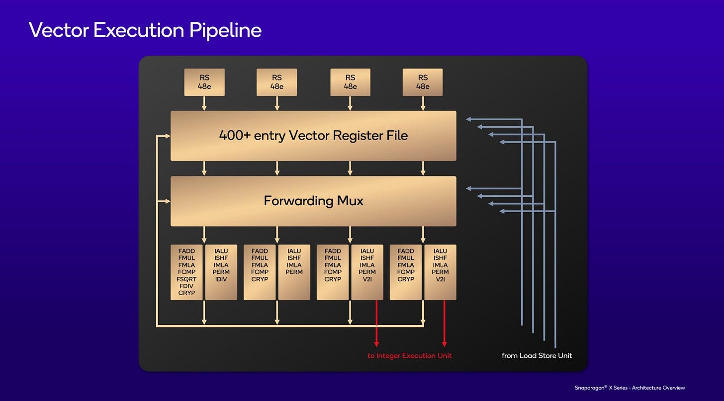
Both the vector and scalar engines have a similar general layout with physical register file. Both have four data feeds from the load/store unit, letting them take four loads per cycle. For comparison, AMD’s Zen 4 can only handle three loads per cycle on the integer side, and two per cycle on the vector side.
Qualcomm has opted for a distributed scheduling model. While there are advantages to unified schedulers, splitting up the queues makes it easier to select the oldest ready instruction.
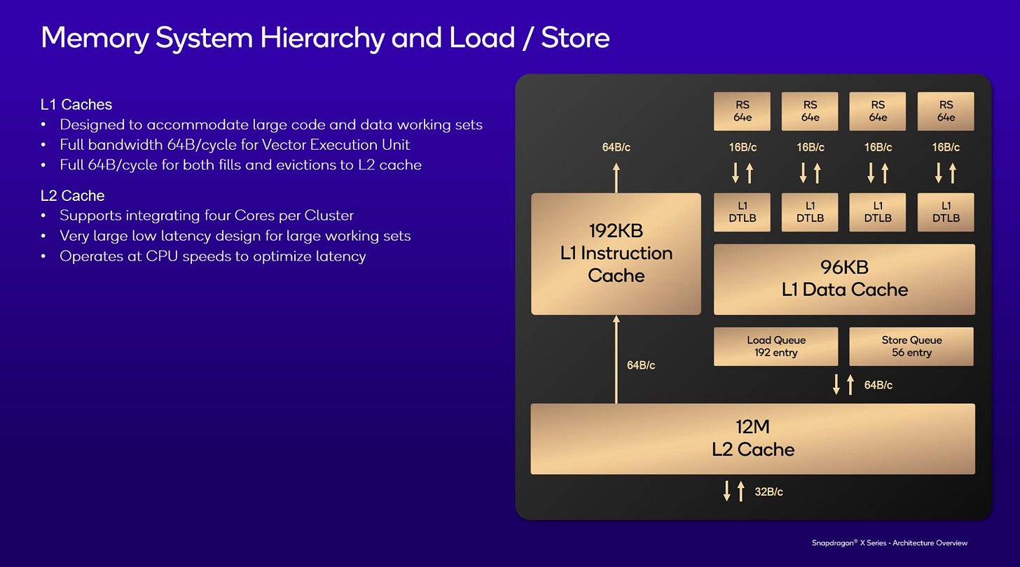
Oryon’s load/store unit has large 64 entry reservation stations, or schedulers. The core has more scheduling capacity than load/store queue capacity, the opposite of what we see in other architectures.
Qualcomm noted that larger schedulers could still meet timing requirements, and relieved some bottlenecks. Furthermore, the schedulers can hold operations other than load/stores (probably store data ops), which the additional capacity helps absorb.
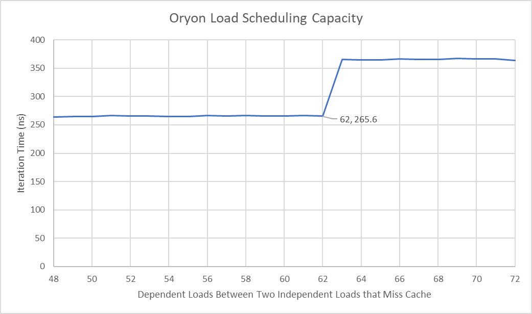
In microbenchmarks, I saw 62 outstanding loads before evidence of a dispatch stall at rename. I took that as an indication Oryon only had 64 total scheduler entries available to loads, but the slides say otherwise.
Perhaps dependent loads run into another limiting structure before scheduler entries are fully utilized. Stores show different behavior and seem to have more scheduling capacity. If stores are implemented as two ops (store address generation and store data), that could be evidence for 256 total RS entries for the load/store unit.
Oryon’s L1 data cache has 96 KB of capacity. It’s multi-ported, and uses standard bitcell designs from the foundry. Qualcomm did evaluate the possibility of using a larger data cache, but a 96 KB design was chosen to meet timing (clock speed) requirements.
TLBs on Oryon are unusually large. Its large 224 entry DTLB was built to balance timing and storage capacity. The L2 TLB has unusually large capacity, because Qualcomm is trying to minimize address translation latency even for large data footprints. Prefetching is also part of this strategy. Oryon tries to bring translations into the TLBs well in advance of a demand access. The extra capacity might reduce the chance of thrashing the TLBs with more aggressive prefetching. In case of L2 TLB misses, Oryon can have 10-20 pending table walks. For perspective, AMD’s Zen 4 could have 6 concurrent page walks.
Testing shows an inflection point at 128 MB, which would correspond to 32768 4K pages. During a separate question and answer session, Gerard Williams implied that was spilling out of the TLB rather than a page walk cache. Therefore, we could be looking at up to 32768 L2 TLB entries. Or, one TLB entry can cover multiple adjacent pages. AMD has done this since Zen, so it’s a distinct possibility. If so, a 8K entry L2 TLB is possible, with each entry covering four pages. Or, it could be a 16K entry structure where each entry can handle two pages. Beyond the L2 TLB, Oryon also has caches in the page table walkers that hold higher level entries in the OS’s translation structures. The size of those structures were not disclosed.
Qualcomm considers Oryon’s 12 MB L2 a very large capacity integrated cache. Latency is 15-20 cycles depending on which part of the cache data is in. That suggests the L2 is built from multiple slices, much like the L3 cache in Intel and AMD’s architectures. Qualcomm says each core has a typical data footprint of 2-3 MB in the L2 cache, though a single core can use the entire 12 MB. The L2 has a 32 byte per cycle interface to the rest of the chip.
I think Qualcomm’s characterization of the L2 cache is accurate. Intel’s E-Cores also share a L2 across a quad core cluster, but use 2 to 4 MB of L2 for the whole cluster. Oryon’s L2 is high capacity in that respect. Crestmont cores in Meteor Lake also have 20 cycle latency to L2, making Oryon’s L2 quite impressive. It has 3-6 times as much capacity, yet maintains the same cycle time latency while being able to clock higher. If each core has a 3-4 MB footprint in L2, the 12 MB of capacity should be adequate even under multithreaded workload. That eliminates the need for a separate layer of cache on the CPU side.
Qualcomm can get a single thread nearly 100 GB/s of DRAM bandwidth thanks to aggressive prefetching, where it’s around 30 GB/s on other cores.
These results largely align with those from my memory bandwidth test. DRAM bandwidth from a single core is definitely much higher than from a Redwood Cove Core in Meteor Lake, though Intel’s core has higher L1 and L2 cache bandwidth.
Past L2, the Snapdragon X Elite has a 6 MB system level cache. Its capacity can be dynamically allocated depending on which block needs it most. The SLC plays a minor role for the CPU cores because it has low capacity compared to the 12 MB CPU L2 caches. However, the SLC is more useful for other blocks on the chip like the GPU and display engine.
Prefetching plays a major role in any remotely modern core. Oryon especially emphasizes prefetching, with a variety of both standard and proprietary prefetchers looking at access patterns and trying to generate requests ahead of instructions asking for the data. Qualcomm shows this off by testing software-visible load latency with various access patterns. Patterns picked up by the prefetcher enjoy lower latency. For a simple linear access pattern, the prefetcher runs far enough ahead to almost completely hide L2 latency.
At the system level, the Snapdragon X Elite has 12 cores in three quad-core clusters. Larger core clusters weren’t used because early in the development lifecycle, clusters with more than four cores weren’t supported by the L2 interconnect. That capability was later added, but didn’t make it into Snapdragon X Elite. We previously noted that the 12 cores were heavily limited by power and thermal constraints in the laptop we tested. In a conversation with the product manager side, they noted that having 12 cores let Snapdragon X Elite scale to higher power targets and provide additional multithreaded performance in devices with better cooling. That strategy contrasts with Intel and AMD, which use different core counts to target a wide range of power targets.
We’d like to thank Qualcomm for giving a very nice presentation on their Oryon core. It’s the first custom Qualcomm core in a long time, and congratulations go out to all the engineers involved in the project. I look forward to seeing Qualcomm evolve the product.
If you like our articles and journalism, and you want to support us in our endeavors, then consider heading over to our Patreon or our PayPal if you want to toss a few bucks our way. If you would like to talk with the Chips and Cheese staff and the people behind the scenes, then consider joining our Discord.


