Intel Details Skymont
Previously Intel’s Skymont slides were published in low resolution, and I wrote a short article on them. Now, the presentation is public with higher resolution slides and presenter audio. Because there’s a lot more detail to comment on, it’s time for a follow up to give a more complete picture of Intel’s presentation.
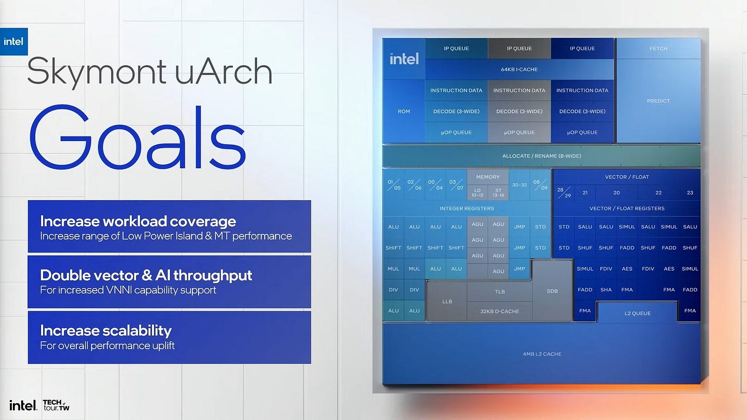
In the context of Lunar Lake, Intel wants to run more applications on the low power island. Crestmont and prior Atom architectures had weaknesses with vector execution and other areas. Skymont aims to address those weaknesses to provide higher performance across a wider range of applications. Those changes also align with Intel’s traditional E-Core goals of providing area-efficient multithreaded performance.
Wide Frontend
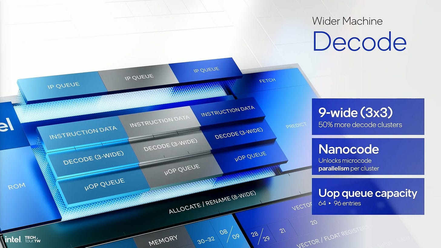
Intel’s Atom line has used a unique clustered frontend since Tremont. Each cluster can fetch 32 bytes per cycle from the instruction cache and decode up to three instructions per cycle. Skymont adds another cluster, letting it fetch 96 bytes per cycle and decode 9 instructions per cycle.
We had the chance to sit down with Stephen Robinson, Intel Fellow and Lead Architect for Intel’s E-cores, to ask some questions. One of the questions we posed to him was, “Why go with the 3 by 3 decode cluster?” To which Stephen said, “It was a statistical bet. And while three 3-wide decoders is a little bit more expensive in terms of the number of transistors then a two by 4-wide decode setup but, it better fits the x86 ISA. In x86 you usually see a branch instruction every 6 instructions with a taken branch every 12 instructions, which better fits the three by 3-wide decode setup Skymont has. A 3-wide decoder is also easier to fill then a 4-wide decoder and having 3 clusters is more flexibly then having 2 clusters hence why Skymont has three 3-wide clusters instead of two 4-wide clusters.”
Micro-ops from the decoders are sent to per-cluster micro-op queues, each with 32 entries. Adding another cluster brings total micro-op queue capacity to 96 entries. More queue capacity lets the frontend run further ahead in case a backend resource fills up. That way, delays in instruction delivery caused by cache misses or slow branch handling can be hidden behind the backend stall. Even with this increase, Intel’s big cores still have more micro-op queue capacity. Redwood Cove has a 192 entry micro-op queue that’s split into two 96 entry portions when two SMT threads are active.
Besides micro-op queues after the decoders, each cluster has instruction byte queues in front of the decoders. Those have increased in capacity by 50% compared to Crestmont. Intel didn’t specify the exact capacity of those queues, but again that lets the frontend run further ahead.
Feeding the Frontend
A wider frontend demands more branch prediction performance. Crestmont already set the foundation for this by having the branch predictor check 128 bytes at a time for taken branches, up from 64 bytes per cycle on Gracemont. However, Crestmont could only do that for 128B aligned blocks. If the starting address isn’t on a 128B boundary, Crestmont couldn’t use its full prediction bandwidth.
Skymont improves by working off 64B cacheline alignment, and is able to scan two 64B cachelines at time regardless of whether the start address is 128B aligned. That should slightly improve frontend bandwidth by letting the branch predictor run further ahead of instruction fetch. In turn, that lets the branch predictor hide BTB latency and initiate L1i fill requests faster to cope with large instruction footprints.
“Nanocode”
From the beginning, Atom cores made heavy use of microcode because power and area constraints prevented designers from adding fast-path hardware for a lot of complex operations. However, reading from the microcode ROM blocks parallel decode. Tremont partially got around this because one cluster could keep decoding simple instructions when the other uses microcode. However, both clusters can’t access microcode at the same time.
Skymont duplicates microcode for the most common complex instructions across all three clusters, letting them handle those instructions without blocking each other. Intel gave gather instructions as an example, which can load from multiple non-contiguous memory locations.
Likely to save area, Intel only gives each cluster enough microcode capacity to handle the most common microcoded instructions. Rarer ones are likely still serviced from a shared microcode ROM.
“Nanocode” is a creative way to increase decode throughput for complex instructions. Other cores can’t do parallel decoding ahead of an instruction that requires microcode. However, those cores also rely less on microcode. Intel’s big cores for example have fast-path gather hardware. They also have complex decoders capable of emitting multiple micro-ops from one instruction without using microcode.
Outside the x86 ecosystem, Apple uses a similar strategy. P-Cores in Apple silicon have an unspecified number of complex decoders capable of emitting up to three micro-ops for a single instruction. Instructions that generate more micro-ops use microcode and does block parallel decoding, but such instructions should be rare. It’s an interesting contrast to Skymont, since both designs try to pack a lot of performance while remaining power and area efficient.
A Much Bigger Backend
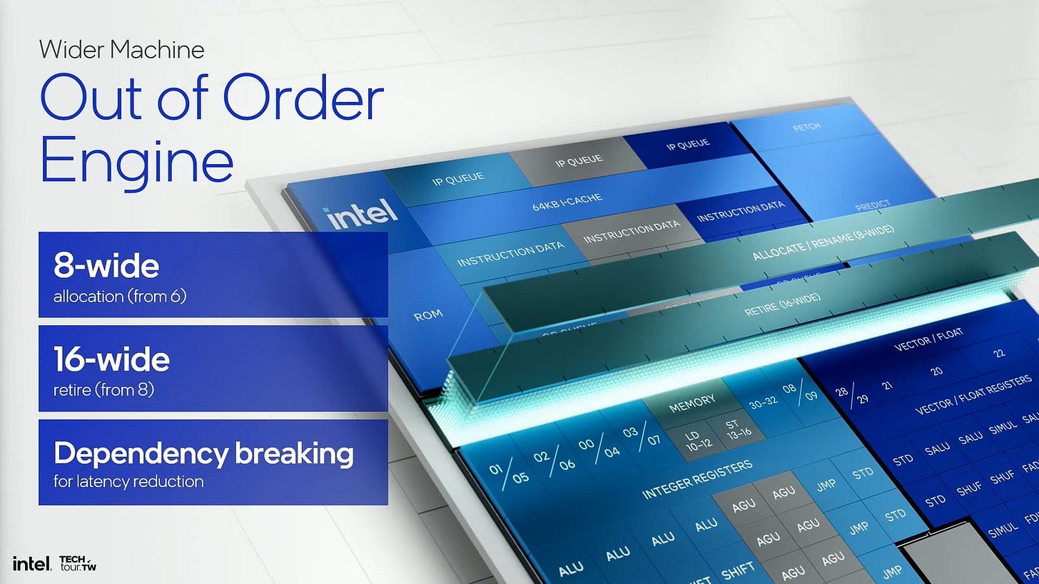
To go with the wider frontend, Skymont sees its rename/allocate stage widened to handle eight micro-ops per cycle. This stage feeds micro-ops into the backend, allocating resources to track them through various stages of execution until their results are made final. It also carries out register renaming and other optimizations to break false dependencies.
Micro-ops exit the backend when they retire, at which point their results are made final and associated backend resources are freed. Skymont widens the retirement stage from 8 to 16 micro-ops per cycle, which feels unbalanced because micro-ops can leave the backend twice as fast as they can enter it. But Intel found they could make various buffers, queues, and register files a bit smaller if they could free up entries in those structures faster. Overall, overbuilding the retirement stage was cheaper than adding more reordering capacity.
Wide retirement has precedent too. AMD’s Zen architecture had 8-wide retire with 5-wide rename/allocate. Before that, Intel’s Skylake could only get four instructions per cycle into the backend, but could retire four instructions per SMT thread. I imagine Intel would have liked to make a wider rename/allocate stage too. But a destination register allocated for one instruction may have to be consumed by a subsequent instruction in the same cycle, so doing wide register renaming sounds a lot harder than doing wide retire.
Along with getting instructions in and out of the backend faster, Intel dramatically scaled up Skymont’s backend. Reorder buffer capacity goes up from 256 entries in Crestmont to 416 entries. Skymont’s register files, load/store queues, and other backend resources get scaled up as well to make the most of the larger out-of-order window. To execute instructions, Skymont gets a massive 26 execution ports.
Intel explains that by saying that dedicated functionality on each port is better for energy efficiency. I’m not sure how this works because more ports will require more register file bandwidth. Perhaps new process nodes allow more register file ports with little power and area overhead, or there’s something else going on. As for why 8 ALUs, Stephen said “It was cheap to add in terms of area and it helps with the peaks.” The peaks refers to when you have code that has a lot of instructions to crunch through.
Skymont’s address generation setup is peculiar because there are four AGUs for store address generation even though the data cache only has enough write bandwidth to service two stores per cycle. Again this feels unbalanced, but having more store AGUs lets Skymont figure out where stores are going sooner. That helps the core figure out whether a load needs to get data from cache or a prior store. Of course Skymont will try to predict whether loads are independent of prior in-flight stores, but figuring out the true result faster helps correct a incorrect prediction before too much work gets wasted.
Wider Vector/FP Execution
Intel’s Atom line historically had weak vector execution. Very limited power and area budgets forced designers to take a narrow focus on lightweight consumer workloads. Vector execution was sacrificed because handling big vectors costs a lot of power and area, while only benefiting a subset of applications.
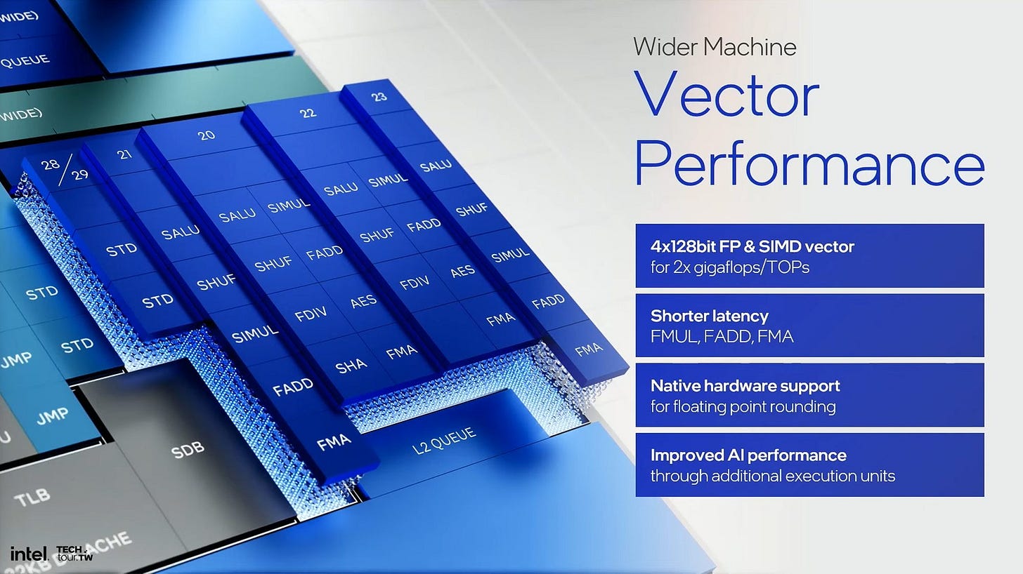
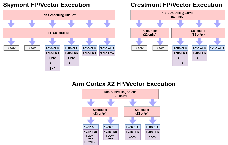
But now, Intel wants E-Cores to perform well across a wider range of applications including ones that use vectors. At the same time, process node improvements allow better vector execution without unacceptable power and area costs. Skymont therefore dramatically increases vector and floating point throughput with 4×128-bit vector execution for the most common floating point and vector integer operations. The resulting setup feels is comparable to the one on Arm’s Cortex X2.
Latency has improved too, with fused multiply-add latency going from six cycles on Crestmont to four cycles in Skymont.
“FP Rounding”
To remove more “glass jaw” cases, where the architecture suffers unexpectedly poor performance because a program does something it wasn’t optimized for, Skymont adds fast path hardware to handle subnormal floating point numbers. Subnormals or denormals are numbers so small they can’t be represented in the standard floating point format. For example, the smallest possible FP32 number is 2-126 because FP32 uses a biased 8-bit exponent with all the unbiased values of 0 and 255 (all 1s) reserved. Smaller numbers can be represented with a subnormal format where all of the exponent bits are 0 and a mantissa that’s interpreted differently. But that extra case requires extra hardware.
Crestmont and prior Atoms handled subnormal values via microcode, which was slow. A FP multiply with a subnormal result costs over 280 cycles on Crestmont. Normal people can get around this performance problem by passing -ffast-math to the gcc compiler. Doing so will cause generated code to set the Flush-to-Zero (FTZ) and Denormals-are-Zero (DAZ). FTZ tells the FPU to treat a result as zero if it’s too small to represent with the normal floating point format. DAZ does the same for inputs to FP operations.
However, some people are not normal and don’t use -ffast-math. Intel specifically called out people who like to use -O2, which doesn’t include the FTZ and DAZ optimizations. With Skymont, Intel has your back even if you’re not normal. As an aside, AMD also doesn’t care whether you’re normal or not. Zen 4 only takes a minor performance hit for denormal results.
A Better Memory Subsystem
Skymont increased throughput, especially on the vector side, will naturally lead to increased bandwidth demands. The L1 data cache can now handle three 128-bit loads per cycle, up from two per cycle on Crestmont. Skymont also increased the miss address buffer entry size from 12 entries on Crestmont to 16 on Skymont which means that Skymont can track more L1 data cache misses compared to Crestmont.
Outside the core, Skymont’s shared L2 cache can provide 128 bytes per cycle of total bandwidth compared to 64 bytes per cycle on Crestmont. Each core is still limited to 64 bytes per cycle of L2 bandwidth, but the L2 can now cope better with bandwidth demands from multiple cores. Lines that get evicted from L2 can be written back to the next memory hierarchy level at 32 bytes per cycle, up from 16 bytes per cycle on Crestmont. That’ll improve memory write bandwidth for workloads that don’t fit in L2.
In Lunar Lake, Skymont benefits from a much better cache setup too. L2 capacity increases to 4 MB compared to Crestmont’s 2 MB, and a 8 MB system level cache helps catch L2 misses. Meteor Lake’s low power Crestmont cores suffered from low last level cache capacity, with just a 2 MB L2. L2 misses faced brutally high LPDDR5X latency, with predictably bad performance as a result. In that prior article, I wondered whether Intel could use a larger L2 or system level cache to achieve their goal of containing more applications on a low power island. Apparently, Intel went for all of the above.
Address Translation
Address translation is an important part of memory performance, since programs use virtual addresses that have to be translated on-the-fly to physical addresses. Skymont’s L2 TLB gets its capacity increased to 4K entries, up from 3K in Crestmont. This huge TLB capacity gives Skymont more TLB coverage than even big cores like Redwood Cove and Zen 4, which have 2K and 3K L2 TLB entries respectively.
On top of increased TLB capacity, Skymont has more page miss handlers. That lets it handle more concurrent page walks in case several instructions miss the L2 TLB in close succession.
Cache Coherency Handling
Gracemont and Crestmont displayed funny characteristics when one core writes data and another core tries to read that data. That’s because Intel used the underlying fabric (a ring bus or Meteor Lake’s Scalable Fabric for example) to handle cache to cache transfers. If a Crestmont core tried to read data modified by another core, it’d be treated as a L2 miss regardless of whether the cores were in the same cluster. This simplified the L2 complex because it wouldn’t need to spend power and area tracking which core had modified what data.
With Skymont, Intel found the power and area budget necessary to let the L2 handle cache-to-cache transfers without involving a lower-level fabric. I’m not sure how Intel did it, but Arm pulled off a similar mechanism in Cortex A72 clusters by maintaining a snoop tag array within the L2 complex. A72’s snoop tag array tracks L1 contents across all core L1 caches in the complex, and is checked with each L2 access. Regardless of implementation details, Skymont should see less off-cluster traffic and improved intra-cluster latency.
Final Words
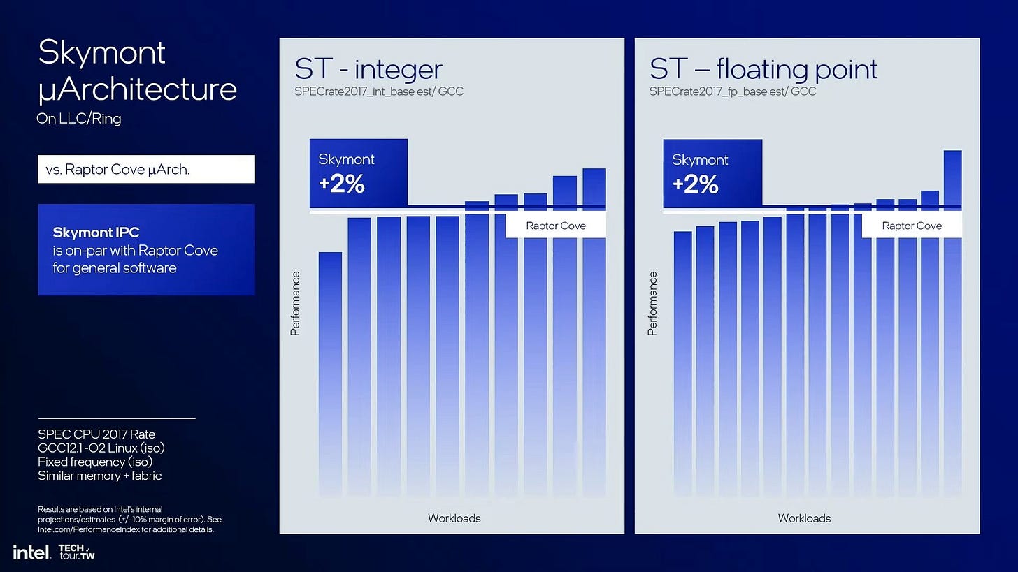
With a clear look at the slides and what the presenter’s saying, Skymont is undoubtedly a major step forward for Intel’s E-Cores. Intel’s Atom line had been closing in on big-core performance per clock for some time. Gracemont was roughly comparable to Skylake, and if Intel’s internal measurements are accurate, Skymont is very close to Redwood Cove in terms of performance per clock. It’s hard to look back at the Atom line’s origins in Bonnell and Silvermont, and imagine what it has become today.
Among nominally low power architectures today, Skymont feels most comparable to Arm’s Cortex X2. Both are very wide cores with ample out-of-order resources, and share traits like 4×128-bit vector execution. Arm does treat Cortex X2 as a flagship high performance core, but it’s important to remember that Arm is attempting to expand upwards out of their core market of fanless cell phones and tablets. Intel in contrast is trying to push power usage downwards in search of longer battery life.
Finally, while Skymont might provide impressive performance per clock, it’s not a high performance core like Intel’s P-Cores. Performance is always achieved by balancing performance per clock with clock speed, and Skymont is unlikely to clock anywhere near what Intel’s P-Cores are capable of. Intel’s P-Core and E-Core lines both still have an important role to play in the company’s hybrid strategy. Developing two different core lines is expensive and complicated compared to AMD’s strategy of using different physical implementations of the same architecture to hit different clock speed and area targets.
Different architecture goals also leads to mismatched instruction set feature support. AVX-512 support is a notable omission on E-Cores. On one hand, it’s an understandable limitation because Atom originated as a very low power CPU. On the other, software doesn’t play nice when different cores on the same CPU don’t support the same ISA features. Intel therefore had to disable AVX-512 support on their P-Cores, a problem that AMD’s strategy avoids. But Intel’s strategy does give them more flexibility to customize each architecture to specific power, performance, and area targets. It’ll be interesting to see how products from both companies stack up once they’re widely available.
If you like our articles and journalism, and you want to support us in our endeavors, then consider heading over to our Patreon or our PayPal if you want to toss a few bucks our way. If you would like to talk with the Chips and Cheese staff and the people behind the scenes, then consider joining our Discord.


