Meteor Lake’s E-Cores: Crestmont Makes Incremental Progress
Efficiency cores, or E-Cores for short, sit front and center in Intel’s consumer CPU strategy. The company introduced E-Cores to its mainstream lineup in Alder Lake, where they sat alongside higher performance P-Cores to improve multithreaded performance while keeping the design area-efficient. Raptor Lake then took the hybrid strategy further, with flagship SKUs featuring twice as many E-Cores as P-Cores. Meteor Lake, Intel’s current mobile offering, doubles down on E-Cores. Its E-Cores move to a new architecture called Crestmont, replacing the Gracemont architecture used in Alder Lake and Raptor Lake. On top of that, Meteor Lake introduces a new low power E-Core category, called LPE-Cores for short. LPE-Cores use the same Crestmont architecture, but change just about everything around it to focus on low power compute rather than performance.
I’ll be testing Crestmont in Intel’s Core Ultra 7 155H using the Asus Zenbook 14 OLED. I’ll primarily focus on differences between Crestmont and Gracemont, Intel’s prior E-Core architecture, using old data from Core i7-12700K and i9-12900K testing. I’ll also discuss details from Intel’s optimization guide.
System Architecture
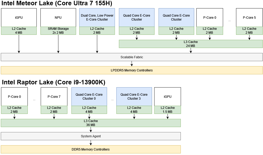
Intel’s Core Ultra 7 155H has eight E-Cores arranged in two quad core clusters. The layout is a lot like Alder Lake’s. Each E-Core cluster interfaces with the ring bus, letting it share a L3 cache with the P-Cores. Two LPE-Cores sit in a separate cluster on Meteor Lake’s SoC tile. Because the LPE-Core cluster doesn’t sit on the ring bus, it doesn’t share the CPU’s L3 cache. While that compromises performance, it lets low power Crestmont handle light tasks without powering up the CPU tile.
Older Intel system architectures use a variation of Sandy Bridge’s system architecture, where the iGPU and all cores sit on a ring bus and share a L3 cache. One ring bus stop leads to the System Agent, which contains a memory controller along with a display controller and miscellaneous IO.
Clock Behavior
Crestmont features a rather dated boost scheme with fixed multi-core boost ratios based on active core count. Loading more than four Crestmont cores drops frequency to 3.1 GHz, with a further decrease to 2.8 GHz if more than six cores are in use. It’s reminiscent of CPUs from the early 2010s. Recent CPUs from Intel and AMD adjust clock speeds based on temperature, power, and current limits instead of setting limits based on active core count. Thankfully, that policy only applies to the Crestmont E-Cores. The P-Cores use a modern boost scheme and can clock independently of the E-Cores.
On the bright side, Crestmont maintains its maximum 3.8 GHz clock with up to four cores active. Core loading order doesn’t matter either. You can get 3.8 GHz with all four cores loaded in a cluster, or two cores loaded from each of the two E-Core clusters. Furthermore, low power E-Cores are managed separately and don’t affect main E-Core boost ratios.
CPU cores also dynamically adjust frequency to save power when they have nothing to do. When work does arrive, Crestmont reaches its maximum 3.8 GHz frequency in just over 5 ms. It doesn’t ramp clock speeds as aggressively as its P-Core partners, but should still deliver good responsiveness.
Unlike desktop cores that head straight to their maximum clock speed with few (if any) intermediate steps, Crestmont takes several steps on the way up. I suspect that lets the power delivery subsystem catch up. Meteor Lake’s low power Crestmont cores increase clocks faster in the first 3-4 milliseconds, but top out at just 2.5 GHz.
Core Architecture Overview
Crestmont is a 6-wide, superscalar, out-of-order core. It’s basically Gracemont with enhancements throughout the pipeline. Both architectures have comparable width to Intel and AMD’s high performance cores, and feature deep reordering capacity to hide memory latency.
I’ve changed some numbers in the diagram compared to Gracemont, but some minor changes are likely due to margin of error and don’t necessarily indicate a core change. Estimating structure sizes through microbenchmarking is not an exact science because the CPU might not reclaim resources immediately on instruction retirement. Real life time commitment is another issue. Dissecting a distributed scheduler requires measuring each scheduler’s size. An unknown scheduler layout adds another dimension of difficulty because I have to figure out whether schedulers are shared by multiple ports.
Intel’s optimization guide says Crestmont and Gracemont serve store data and jump operations with the same queue. I missed this in 2021 because that possibility didn’t cross my mind.
Frontend: Branch Prediction
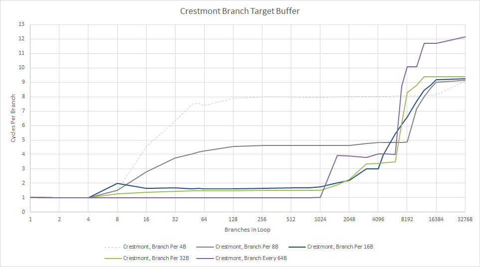
Branch prediction is vital to both performance and power efficiency. Accurate branch prediction reduces wasted work, while faster prediction helps keep the core fed with instructions. Crestmont’s branch predictor gets tweaks in both areas. The branch target buffer (BTB) gets a capacity boost from 5120 to 6144 entries, letting the core remember more recently used branch destinations. I’ll refer to this as the L2 BTB, since Gracemont and Crestmont both have a 1024 entry first level BTB that can handle taken branches with single cycle latency.
Intel had to increase L2 BTB latency to achieve that capacity increase. Furthermore, Crestmont seems to do best when branches are spaced out by 64B. With one branch every 64 bytes, the L2 BTB on Crestmont can provide a taken branch target once every four cycles. I never tested that case on Gracemont, but Gracemont’s L2 BTB could handle a taken branch about once every three cycles.
Intel’s optimization guide says Crestmont’s branch predictor can scan up to 128 bytes per cycle to find branches and make predictions, compared to 32 bytes per cycle on Gracemont. I don’t have a way to measure this, but it could let the branch predictor run further ahead of the fetch and decode stages to mitigate higher L2 BTB latency.
Branch predictor accuracy is important too. Intel says Crestmont has “Enhanced Path Based Branch Prediction”. I don’t have tests written to directly go after branch predictor parameters like history register length. But throwing a simpler test that varies branch count and random pattern length per branch shows that Crestmont can cope with longer patterns than Gracemont.
With just a few branches in play, Crestmont sees very little mispredict penalty even when each branch is taken/not taken in a 2048-long pattern. Gracemont started seeing mispredict penalties after 1536.
In any case, both predictors are very capable and competitive with older Intel big cores. Crestmont’s slight improvements over Gracemont are welcome, even if it’s not a full-generation jump.
Frontend: Fetch and Decode
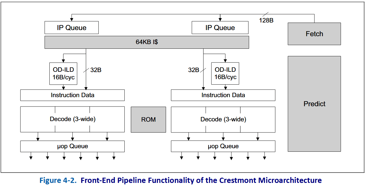
After determining where to go, the frontend has to fetch instructions from memory and decode them into an internal format. First, virtual addresses are translated to physical ones using a 64 entry instruction TLB. Then, instruction bytes are fetched from a 64 KB instruction cache and passed to the decoders.
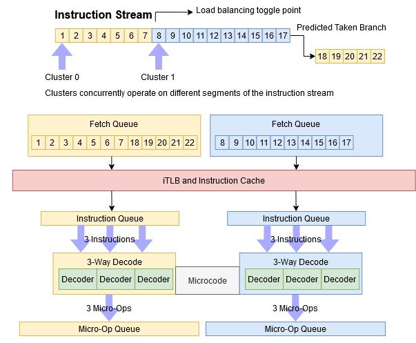
Like Gracemont and Tremont before it, Crestmont’s frontend is split into two fetch and decode pipelines. Each can fetch 16 bytes and decode three instructions per cycle, and operates independently of the other. As on Gracemont, Crestmont’s branch predictor alternates between feeding each cluster’s fetch target queue, and tries to load balance between them. This load balancing makes the clustered decoders behave much like a traditional 6-wide one. Even if you massively unroll a loop and create a giant basic block of doom, Crestmont’s frontend will happily plow through it at 6 instructions per cycle.
With 4 byte instructions, Crestmont generally enjoys better frontend throughput than Gracemont. Code that fits within L1i benefits from Crestmont’s wider renamer (more on that later), which can handle 6 instructions per cycle. Instruction cache misses get queued into an 8 entry miss buffer, which does a good job of hiding L2 and L3 cache latency. Throughput impressively stays above 4 IPC when running code from L2. IPC drops as code spills into L3, but Crestmont still stays ahead of Gracemont.
Low power Crestmont enjoys similar instruction throughput from L1 and L2, but doesn’t share the 24 MB L3 cache used by the main E-Cores and P-Cores. After a L2 miss, low power Crestmont has to fetch instructions from painfully slow main memory.
x86 instructions are variable length, and long instructions can move the bottleneck from decode width to instruction cache bandwidth. With 8B NOPs, Crestmont can fetch 32 bytes per cycle. Again Crestmont outperforms Gracemont when running code from L2 and L3. And again, low power Crestmont exhibits similar per-cycle behavior.
Rename and Allocate
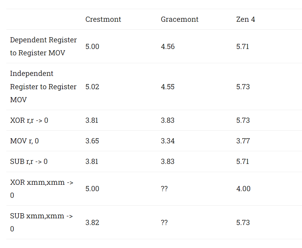
After the frontend gets instructions fetched and translated, the renamer has to allocate backend resources. It also performs register renaming to remove false dependencies, and can pull a few other tricks to expose extra parallelism. Crestmont’s renamer can handle 6 instructions per cycle, letting the core take full advantage of its frontend throughput. Gracemont in contrast was capped at 5 instructions per cycle. Crestmont can also perform various optimization tricks at a higher rate, though not at the full 6 per cycle rate.
Register to register MOVs can be eliminated at 5 per cycle. Crestmont can recognize operations that always result in zero, like XOR-ing a register with itself or subtracting a register from itself. However, it can’t completely eliminate them and still has to allocate physical registers. The 4 per cycle throughput also suggests those operations still need an ALU pipe to zero the register. Strangely, Crestmont can eliminate zeroing vector XMM registers at 4-5 per cycle. Crestmont only has three vector execution pipes, so the renamer is able to zero vector registers by itself.
Allocation reads the uop queues of all front-end clusters simultaneously and generates an in-order stream splicing across clustering boundaries within the same cycle as necessary.
Intel 64 and IA-32 Architectures Optimization Reference Manual
Previously I assumed Gracemont and Crestmont’s renamers could only feed from one cluster’s micro-op queue each cycle. That would simplify hardware because the renamer would only have to update state for one queue at a time. Evidently Intel thought renamer throughput was important enough to let the renamer pull micro-ops from both clusters in the same cycle. Putting those micro-ops back into program order for renaming involves extra complexity too.
Crestmont/Gracemont’s renamer can also perform micro-op splitting, most notably splitting 256-bit vector operations into two 128-bit halves. A lot of CPUs do such splitting at the decoders, but moving it further down the pipeline to the rename stage helps conserve decode bandwidth and make better use of the micro-op queues.
Out of Order Execution
Once micro-ops flow into the backend, they’re tracked and executed as their dependencies become available. Crestmont has the same scheduler layout and execution resources as Gracemont, though Intel may have added a few more scheduler entries on the floating point side. Specifically, the scheduler for floating point and vector stores grows from 18 to 22 entries, and the floating point math scheduler gets a bump from 35 to 38 entries.
Intel also improved the floating point divider. Latency seems to be cut in half from Gracemont, from 10 cycles (uops.info data) to 5. They added another vector integer multiplier too, though I’m not sure which instruction it applies to. Packed INT32 multiplies aren’t included.
Those changes should make Crestmont slightly stronger in floating point and vector workloads, but won’t change the big picture. Crestmont’s renamed register files, load/store queues, and reorder buffer appear unchanged compared to Gracemont. Much of what I wrote in the previous Gracemont article still applies.
Address Translation
Programs running on modern CPUs don’t directly address locations in physical memory. Instead, they use virtual addresses that get translated to physical memory locations by page tables set up by the operating system. That lets the operating system give each program an isolated view of memory, preventing a misbehaving application from bringing the entire system down. But that means one virtual memory access could turn into several dependent memory accesses. CPUs avoid this by caching recently used translations in structures called Translation Lookaside Buffers (TLBs).
Crestmont and Gracemont both have a 48 entry fully associative L1 DTLB, but Crestmont increases L2 TLB size from 2048 entries to 3072. More TLB coverage will let Crestmont keep effective memory access latency low for programs with larger memory footprints. Associativity also increases from 4-way to 6-way, reducing the chance of TLB conflict misses.
Intel keeps latency the same at 9 extra cycles to get a translation from the L2 TLB. As on Gracemont, it’s a lot of cycles especially for a slow-clocked core. But at least it didn’t get worse.
Memory Disambiguation
Load/store units in modern CPUs have the challenging task of ensuring memory accesses appear to execute as specified by the programmer, even when the backend has many in-flight accesses that might hit the same address. Specifically, loads might have to get their data from an earlier overlapping store. Comparing every load address with every prior store address can get pretty expensive, and partial overlap cases get complex fast. Therefore, engineers take shortcuts to reduce hardware cost while (hopefully) maintaining high performance for the most common memory dependence cases.
Crestmont behaves like Gracemont and can only forward the upper or lower half of a store to a dependent load. However, Intel optimized the most common exact address match case. It’s not quite “free” store to load forwarding like with Golden Cove or Zen 3, but Crestmont seems to have a fast path for exact address matches with a latency of 1-3 cycles. Forwarding the upper half of a store to a dependent load has 6 cycle latency. Other overlap cases cause a 11-12 cycle penalty, which increases to 12-13 cycles if both accesses cross a 64B cacheline.
Like Gracemont, Crestmont suffers page crossing penalties. Loads take a 15 cycle penalty if they cross a 4K page, and stores take a 33 cycle penalty. Intel and AMD’s higher performance CPUs can handle page crossing loads with minor or no penalties, though stores can still be nasty.
Cache and Memory Latency
Crestmont and Gracemont have very similar cache hierarchies, though Crestmont may have changed the L2 replacement policy to something non-LRU. L3 latency remains high, and the core continues to rely on a 2 MB L2 to keep memory accesses off the slow ring bus.
Low power Crestmont doesn’t have a L3, so its 2 MB L2 serves as a last level cache. 2 MB is very small for a last level cache, so Meteor Lake’s LPE-Cores will be very susceptible to losing performance from hitting DRAM.
Clock speeds matter too, because they affect actual latency. Low power Crestmont’s low clocks mean that L2 latency is only slightly better than Zen 2’s L3 latency.
Memory latency on Meteor Lake is rather high. LPDDR5 plays a factor, but AMD chips like Van Gogh and Phoenix manage to keep latency under 200 ns with 2 MB pages.
Cache and Memory Bandwidth
Crestmont and Gracemont aren’t optimized for long vectors and natively use 128-bit load/store paths. 256-bit AVX accesses don’t provide higher bandwidth than 128-bit SSE ones. However, Crestmont can achieve decent L1D bandwidth thanks to four memory access pipelines. Two pipes handle reads, while the other two handle writes. With an even mix of reads and writes, Crestmont can sustain 64 bytes per cycle of L1D bandwidth.
After L1, Crestmont shares a 2 MB L2 with other cores in the same cluster. A single core can get just below 32 bytes per cycle from L2, possibly limited by how fast the L1D can service fills and accesses from the core. Then, E-Core Crestmonts share a 24 MB L3 with other E-Core clusters and P-Cores. L3 bandwidth from a single Crestmont core is pretty bad at 10-12 bytes per cycle.
Low power Crestmont has everything worse because it runs at lower clock speeds and doesn’t share the 24 MB L3 cache. Its bandwidth characteristics are closer to that of a cell phone core from several years ago than any standard laptop or desktop core.

A Cortex A76 on the Snapdragon 855 has about the same L1 bandwidth as low power Crestmont, though Crestmont’s L2 does provide good per-core bandwidth for a shared cache. The Snapdragon 855 only has 256 KB L2 caches for its A76 cores, and bandwidth from its 2 MB CPU L3 is downright poor. But that’s a story for another day.
Multi-Core Bandwidth
Loading more cores will increase pressure on shared caches, and Crestmont has two levels of shared caches. The cluster-level L2 cache can supply 64 bytes per cycle. L2 misses are tracked in a 64 entry queue and get data from the cluster’s ring bus interface.
I was able to get 341 GB/s of L2 bandwidth from Crestmont by loading two cores per cluster. Loading more than four cores cores lowers clock speeds, which also reduces available L2 bandwidth. L3 read bandwidth is a modest 115 GB/s, achieved again by loading two cores per cluster to maximize clocks. Meteor Lake might have a new E-Core architecture and system level design, but bandwidth characteristics are eerily reminiscent of what I saw in Alder Lake years ago. There, Gracemont was also limited to 115 GB/s from L3, or less than 32 bytes per core clock across both clusters. Intel’s ring bus stops should be capable of sinking 32 bytes per cycle since Sandy Bridge, so I’m not sure why Gracemont clusters seem capped at 16 bytes per cycle.
Meteor Lake’s LPDDR5 may have high theoretical bandwidth, but getting that from the E-Cores will be hard thanks to high latency. The two Crestmont clusters can read from main memory at just under 40 GB/s, a regression compared to the 60 GB/s that Gracemont achieved on the 12900K. Mixing in writes can get around latency to some extent because a write can likely be considered complete once it’s handed off to the cache hierarchy. The core doesn’t have to track the request until data returns like with reads.
A quad core Crestmont cluster get almost 60 GB/s with non-temporal writes, which likely moves the bottleneck back to the ring stop. Low power Crestmont has a much harder time achieving good DRAM bandwidth, perhaps indicating a slower link to Meteor Lake’s interconnect or fewer queue entries.
Core to Core Latency
A CPU’s interconnect has to ensure all cores have a coherent view of memory, even though cores by default try to keep accesses within their private caches to improve performance. If a core needs data that’s written by another core, it’ll need data transferred between core-private caches, rather than getting loaded from shared cache or DRAM. We can measure latency for these accesses by bouncing a cacheline between a pair of cores, with the cores taking turns writing and reading.
Meteor Lake’s E-Cores behave like the ones on Alder Lake. Coherency is handled at the ring bus. Core-to-core transfers within an E-Core cluster take longer than crossing cluster boundaries, possibly because that requires a full round trip on the ring. The low power E-Cores aren’t ring bus clients, and rely on Meteor Lake’s Scalable Fabric to handle coherency. They suffer far higher latency. It’s like going between clusters on AWS’s Graviton 1.
Final Words
Intel’s Atom line has come a long way from being low power afterthoughts to earning a place alongside Intel’s high performance cores in mainstream client designs. Tremont and Gracemont are notable milestones on Atom’s journey. Tremont marked a shift that saw Atom transform into a much bigger core. Gracemont went even bigger, fixed some rough edges, and added AVX2 support to improve the hybrid core situation. Crestmont shows up more than two years after Gracemont, but doesn’t make the same kind of splash. Its wider renamer, larger L2 TLB, and better branch predictor are welcome of course. But major structures like the register files, load/store queues, and reorder buffer remain untouched, making Crestmont a very conservative step.
Intel has good reason to be conservative. Meteor Lake is a pandora’s box of engineering challenges. It shifts from Intel’s tried and true monolithic die strategy to using chiplets, some of which use TSMC nodes instead of Intel ones. It discards the Sandy Bridge system architecture that had been in place since 2011. It adds a new NPU and a new iGPU architecture.
Crestmont jumps into that storm of change to fill both E-Core and LPE-Core roles. Validating Crestmont across two different physical implementations with different interfaces to the rest of the system is a considerable challenge too. I find it amazing that Intel got Meteor Lake out the door with all those parallel engineering efforts. It’s also a testament to company leadership recognizing engineers have limited time, sanity, and coffee. Trying to pull off Meteor Lake with more ambitious CPU architectures changes could have led to disaster.
Meteor Lake doesn’t exist in isolation and AMD’s Phoenix APU presents strong competition. Phoenix uses a monolithic die and largely carries forward the system architecture from prior AMD mobile designs. A smaller Phoenix variant does mix density optimized Zen 4c cores with standard high performance Zen 4 ones. But both core variants use the same architecture. Thus AMD is not concurrently evolving two CPU architectures, creating a triple-level hybrid design, and fitting a chiplet design within a power constrained mobile platform. Instead of solving a batch of hard problems, Phoenix avoids them.
AMD instead spends engineering bandwidth on CPU architecture. Zen 4 is a big step over Zen 3, with increased reordering capacity, AVX-512 support, and branch predictor improvements. Intel may have an impressively large workforce with 124,800 employees in 2023. AMD for comparison had 34,648 employees in 2022. But even Intel isn’t immune to opportunity cost, and a hypothetical better Crestmont might be part of that cost. Today, Crestmont inherits many of Gracemont’s 2021 shortcomings. No AVX-512 support prevents Intel from rolling out AVX-512 capable client chips, even though P-Cores can handle it. L3 performance isn’t great. DTLB capacity is a bit low at 48 entries, and L2 TLB latency is high.
Now that Intel has done their system level architecture switch, I look forward to seeing what they do with Crestmont’s successor. Intel has a ton of engineering power at their disposal, and I hope their leadership uses it well.
If you like our articles and journalism, and you want to support us in our endeavors, then consider heading over to our Patreon or our PayPal if you want to toss a few bucks our way. If you would like to talk with the Chips and Cheese staff and the people behind the scenes, then consider joining our Discord.


