Hackaday recently published an article titled “Why x86 Needs to Die” – the latest addition in a long-running RISC vs CISC debate. Rather than x86 needing to die, I believe the RISC vs CISC debate needs to die. It should’ve died a long time ago. And by long, I mean really long.
About a decade ago, a college professor asked if I knew about the RISC vs CISC debate. I did not. When I asked further, he said RISC aimed for simpler instructions in the hope that simpler hardware implementations would run faster. While my memory of this short, ancient conversation is not perfect, I do recall that he also mentioned the whole debate had already become irrelevant by then: ISA differences were swept aside by the resources a company could put behind designing a chip. This is the fundamental reason why the RISC vs CISC debate remains irrelevant today. Architecture design and implementation matter so much more than the instruction set in play.
Some Key Terms
- CISC and RISC
- CISC stands for Complex Instruction Set Computer. Historically, the CISC philosophy aimed to accomplish a task with fewer, more complex instructions. In the 1970s, the x86 instruction set was designed with the CISC philosophy in mind.
- In contrast, the Reduced Instruction Set Computer (RISC) philosophy wanted to use fewer and simpler instructions to make hardware design easier. Hopefully simpler hardware could run faster and be more performant. MIPS and ARM were originally designed following the RISC philosophy in the 1980s.
- Superscalar
- A superscalar CPU can execute more than one instruction per clock cycle, in contrast to a scalar one that can only execute one instruction at a time.
- Out-of-order execution
- A CPU with out-of-order execution can internally execute instructions as their dependencies become ready, irrespective of program order. It means independent instructions can begin execution ahead of a stalled one, improving execution unit utilization and mitigating the impact of cache and memory latency.
But What Are Modern CPUs Really Like?
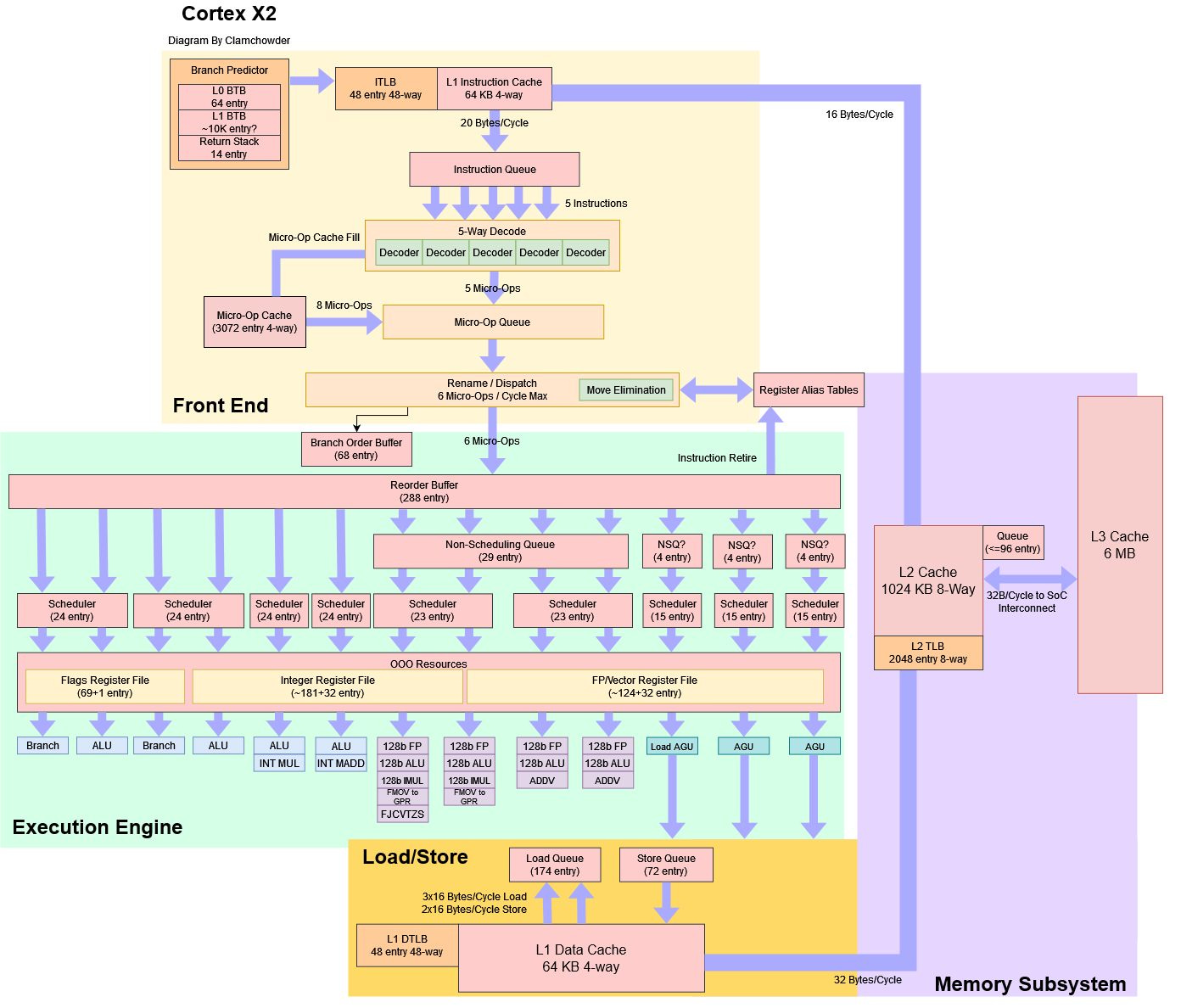
Here are block diagrams outlining the microarchitecture of two unrelated CPUs, developed by different companies, running different instruction sets. Neither CPU core is simple, but both have a lot in common.
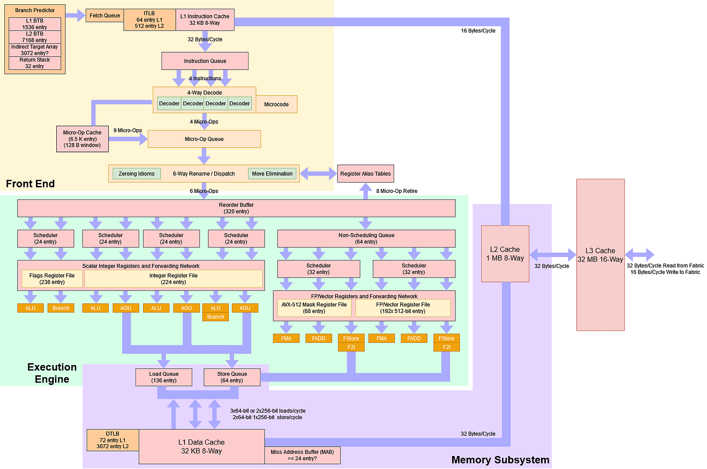
Cortex X2 and Zen 4 both use superscalar, speculative, out-of-order execution with register renaming. Beyond the core, both Cortex X2 and Zen 4 use complex, multi-level cache hierarchies and prefetchers to avoid DRAM access penalties. All of these features have everything to do with maximizing performance, especially as compute performance keeps outpacing DRAM performance. They have nothing to do with the instruction set in play.
Where the Problem Doesn’t Lie
Hackaday mentions the complexity of fetching and decoding instructions, but this isn’t a problem unique to x86. No modern, high-performance x86 or ARM/MIPS/Loongarch/RISC-V CPU directly uses instruction bits to control execution hardware like the MOS 6502 from the 1970s. Instead, they all decode instructions into an internal format understood by the out-of-order execution engine and its functional units.
Decoding is expensive for RISC architectures too, even if they used fixed length instructions. Like Intel and AMD, Arm mitigates decode costs by using a micro-op cache to hold recently used instructions in the decoded internal format. Some Arm cores go further and store instructions in a longer, intermediate format within the L1 instruction cache. That moves some decode stages to the instruction cache fill stage, taking them out of the hotter fetch+decode stages. Many Arm cores combine such a “predecode” technique with a micro-op cache. Decode is expensive for everyone, and everyone takes measures to mitigate decode costs. x86 isn’t alone in this area.
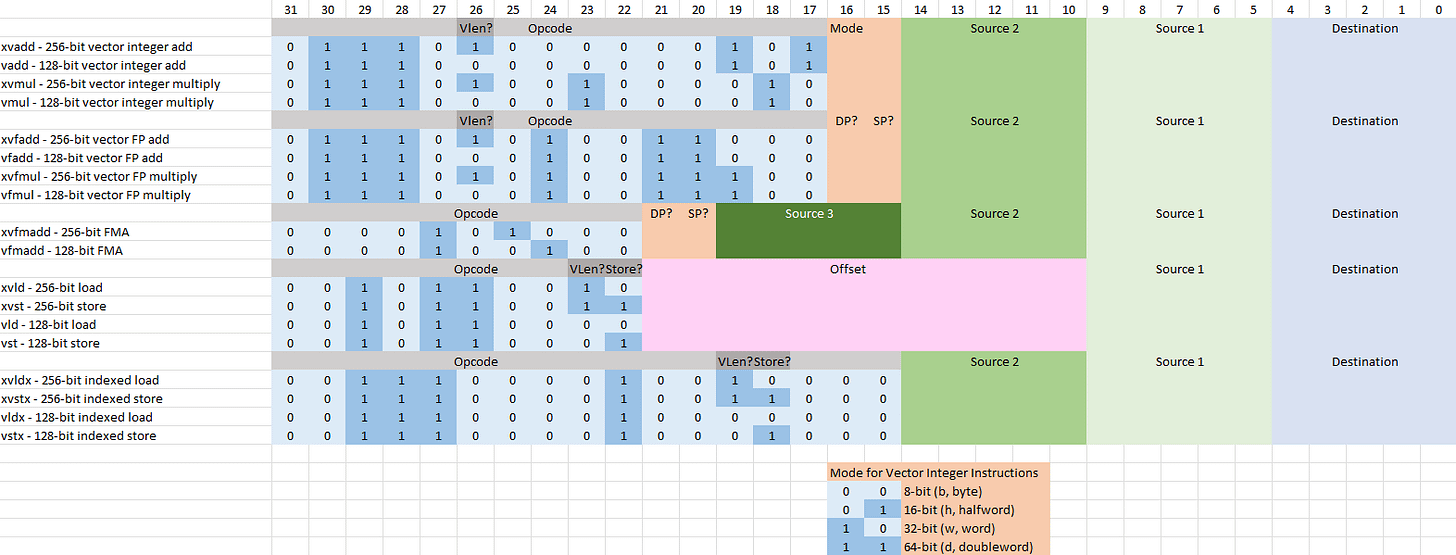
Hackaday further takes issue with instruction set extensions and increasing instruction count, but neither are distinctly x86 features. ARM has similarly been through numerous revisions and extensions. Where x86-64 has SSE, AVX(2), and AVX-512 vector extensions, 64-bit ARM (aarch64) has ASIMD, SVE, and SVE2 vector extensions. MIPS has a similar story with a MSA SIMD extension. MIPS didn’t get more extensions as ARM and x86 did, but that’s because no one was using it anymore. LoongArch is derived from 64-bit MIPS, but uses incompatible instruction encodings. Loongson has extended LoongArch with the LSX and LASX vector extensions.
ISAs also receive updates that have nothing to do with vectors. aarch64 got updates to accelerate atomic memory operations and speed up `memcpy`/`memset` routines. x86 sees similar updates from time to time, though in different areas. That’s because more transistor budget lets engineers do more things in hardware, and adding more instructions for specific workloads is a great way to speed them up.
mpsadbw
is fine
Next, Hackaday focuses on x86’s mpsadbw
instruction, noting that it’s doing “at least 19 additions but the CPU runs it in just two clock cycles.” The author should think of why that instruction exists by looking at its use cases. Video codecs strive to efficiently use bandwidth and disk space by representing most frames in terms of how they differ from previous ones, rather than storing the entire frame. Calculating the sum of absolute differences (SAD) is a good way to see how much a block has changed, and is a vital part of video encoding. ARM has similar vector instructions.
The author then suggests adding more instructions (like mpsadbw
) makes register renaming and instruction scheduling more complex. That makes intuitive sense, but doesn’t match reality. Even though mpsadbw
does more low-level operations, it only requires two register inputs and one destination register. The renamer therefore only needs to read two values from the register alias table to determine where to get inputs from, and allocate one free register to store the result.
The author looked at an instruction, noted that it does multiple calculations, and therefore concludes it looks scary, but let’s consider the alternative. We can perform the vector SAD calculation with RISC-like instructions (excluding the selection part of mpsadbw
). Each simple RISC instruction would require the same degree of register renaming as the “complex” msadbw
instruction. Each input requires a lookup in the register alias table, and a free register has to be allocated to hold each result.
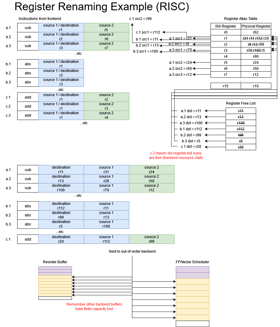
Contrary to the author’s claims, complex instructions actually lower register renaming and scheduling costs. Handling an equivalent sequence of simple instructions would require far more register renaming and scheduling work. A hypothetical pure RISC core would need to use some combination of higher clocks or a wider renamer to achieve comparable performance. Neither is easy. As shown above, the same register may be renamed multiple times in quick succession, so a wider renamer must cope with a longer potential dependency chain. Beyond a wider renamer, a pure RISC design would need larger register files, schedulers, and other backend buffers to mitigate the impact of having to track more instructions.
Changes Have Already Come
Of course, people designing ARM CPUs understand the importance of efficiently using fetch/decode/rename bandwidth. They also understand the importance of economizing usage of backend resources like register files and scheduler entries. That’s why ARM today has plenty of complex instructions that perform many low-level operations under the hood. Vector instructions may be the most prominent example, but it’s easy to find other examples, too. aarch64 has long supported loading a value from memory with an address generated by shifting an index register, and adding that to a base register. That’s a chain of three dependent operations under the hood, but it simplifies array addressing.
On the other side, simple instructions often make up the majority of an executed program’s instruction stream. That’s especially applicable for programs that are hard to parallelize, like file compression or web browsing. CPUs today therefore have to be good at executing simple operations quickly. At the same time, they benefit from having complex instructions to speed up specific workloads.
Instruction sets today have changed with that reality in mind. The “CISC” and “RISC” monikers only reflect an instruction set’s distant origin. They reflect philosophical debates that were barely relevant more than three decades ago, and are completely irrelevant now. It’s time to let the CISC vs RISC debate die, forever.
Where Problems Actually Lie
Hackaday mentions x86’s real mode, leading to another important point: compatibility. When gushing over different CPUs and the performance they offer, it’s all too easy to forget what that performance is needed for: running software. If a CPU doesn’t run the software you need, it’s a tiny brick. x86-64 CPUs keep real mode around so that operating systems can keep booting in the same way. Today, you can create a single OS install drive that works on a modern Zen 4 system, a Phenom system from 15 years ago (just make sure you use MBR boot) and everything in between. That 15-year-old Phenom system can run recent operating systems like Windows 10 or Ubuntu 22.04. Of course there are limits, and you can’t run Windows 10 out of the box on a Northwood Pentium 4. But real mode support is part of what makes the same OS boot code work across so many CPUs. It’s part of the PC compatibility ecosystem that gives x86 CPUs unmatched compatibility and longevity.
Other ecosystems present a sharp contrast. Different cell phones require customized images, even if they’re from the same manufacturer and released just a few years apart. OS updates involve building and validating OS images for every device, placing a huge burden on phone makers. Therefore, ARM-based smartphones fall out of support and become e-waste long before their hardware performance becomes inadequate. Users can sometimes keep their devices up to date for a few more years if they unlock the bootloader and use community-supported images such as LineageOS, but that’s far from ideal.
Intel and AMD correctly realized that spending extra effort on compatibility is worthwhile. Doing so streamlines software distribution, and lets users hang onto their expensive hardware for longer.
Of course, compatibility can’t be maintained forever. ISAs have to evolve. AMD and Intel probably want to save some money by reducing the validation work needed to support real mode. Intel is already planning to drop real mode. Any ISA has to receive updates as requirements change over time. But compatibility breaks should be kept to a minimum, to avoid shoving users onto an upgrade treadmill with no clear benefit.
Conclusion
The CISC vs RISC debate seems to reignite every few years, often with claims that x86 should die. That debate was most compelling in the early 1990s while I was learning to walk. Alpha’s EV5, for instance, was a four-wide core from 1994 that ran at 266 MHz. Intel’s best 1994 CPU was the two-wide, 120 MHz Pentium. But soon Intel showed they could develop high performance designs of their own, and we know what happened by the end of the decade.
The 2000s saw Intel themselves try to push x86 to the side. Itanium was designed around the principles Hackaday’s author believes so strongly in. It used a set of 128 architectural registers to avoid register renaming. It used simple, fixed-length instructions. It dropped out-of-order execution to move scheduling responsibilities to the compiler. All of those ideas failed because increasing transistor budgets allowed better branch prediction and larger out-of-order execution structures. Hardware out of order execution could adapt to changing program behavior and naturally generate more optimal instruction schedules. Since out-of-order execution was necessary for high performance anyway, there was little point in keeping Itanium around.
Toward the late 2010s, Marvell’s ThunderX3 and Qualcomm’s Centriq server CPUs tried to find a foothold in the server market. Both used aarch64, and both were terminated by the end of the decade with little to show for their efforts. That’s not to say aarch64 is a bad ISA, or that ThunderX3/Centriq were doomed by it. Rather, a CPU needs to combine high performance with a strong software ecosystem to support it.
Today, aarch64 has a stronger software ecosystem and better performing CPU cores. Ampere Altra chips are deployed across Google, Microsoft, and Oracle’s public cloud offerings. Amazon is also using Arm’s Neoverse cores in their cloud. aarch64 is in a place where it can compete head on with x86 and challenge the Intel/AMD duopoly, and that’s a good thing. But Arm, RISC-V, and MIPS/LoongArch will have to succeed through the merits of their hardware design and software ecosystems. All of those instruction sets are equal enough in areas that matter.
Going forward, I hope we’ll have more productive, well-researched discussions on the merits of various CPU designs. Of course, ISA can be part of the debate, as various ISA extensions can have a tangible impact on performance. Licensing and royalties should also be discussed, as both regularly kill all sorts of promising technologies. But utterly incorrect claims like “In RISC architectures like MIPS, ARM, or RISC-V, the implementation of instructions is all hardware” need to get thrown out. The year isn’t 1980 anymore.
If you like our articles and journalism, and you want to support us in our endeavors, then consider heading over to our Patreon or our PayPal if you want to toss a few bucks our way. If you would like to talk with the Chips and Cheese staff and the people behind the scenes, then consider joining our Discord.
I largely agree with this article, of course, but if I may add two cents:
* A nice thing about RISC-V specifically is that the base ISA scales from tiny microcontrollers all the way up to high-performance cores, and I think to say it’s fair to say that that’s a virtue of the ISA. I think it would be harder to do so with x86, at least with the same performance on the small implementations.
* Branch-and-link feels nicer than CALL/RET in that leaf calls don’t *necessarily* need to cause memory accesses. It probably doesn’t make a big difference in practice, but CALL/RET just feel so inefficient in comparison.
* It seems to me that if x86 has any real disadvantage, it has to be the memory model. For example, various benchmarks seem to show that the required reads-for-ownership can actually impact performance a lot in certain (narrow) scenarios, and architects surely have to expend a lot of arguably unnecessary effort on speculating around the memory model.
* It would be harder to use modern x86-64 in a microcontroller since supporting stuff like SSE would be overkill, but you could use something closer to the original 1980s x86 ISA in one. The Airbus A320 for example uses a 80186 as a microcontroller.
* I’m torn on that. If you don’t have nested function calls, then sure. But once you do, you have to save the previous return address somewhere.
* If you mean total store ordering, I think not having TSO only avoids RFOs in very narrow scenarios, where you lose lock on a cacheline while a store to it is in-flight. On the flip side, you may be able to avoid using a possibly expensive explicit lock if TSO is enough to ensure correct behavior.
FWIW, Intel already tried x86 (32-bit) in a microcontroller. They called it Quark (2013-2019) and used it to target the IoT market. When all you’ve got is a hammer…
x86’s greatest advantage is the ability to adopt the technology du jour (even if it’s a suboptimal design).
For example,AMD64 was great and all (big address space, inefficient Rex encoding, and the always amusing movabsq) or shoehorning virtualization into x86. Right set of features (at a reasonable price point) to make cloud computing work.
The incrementalism of x86 virtualization makes you know it’s an x86 feature. VMX, EPT, one billion small VMX controls later you have something pretty powerful.
I don’t think anyone had cloud computing in mind when AMD64 came around. But yeah everyone adopts features when they think it’s important enough. Arm CPUs for example added atomic compare-and-swap, support for vectors wider than 128 bits, and instruction cache coherency. So they’re also adopting technology when they feel it’s needed to serve their market segments.
The smart phone comparison is a red herring here. A lack of standardization for board initialization code, 5+ major CPU vendors all vying for artificial differentiation above and beyond the Arm Ltd specs, GPU drivers with artificial vendor specific extensions, screen differences, etc is what leads to firmware image proliferation. If you added in the main board initialization code for PCs into an atomic whole paired with the OS itself you’d end up with the same headache. Each main board revision (example an ASUS model X1 versus model X1 rev. 2) would require its own OS firmware image, too. Standardization has obscured most of those differences in the PC realm to end users except when it comes to screen ratios not adhering to the common 16:9 😉 Apple shows how it could be when it comes to Arm based desktop class systems. Whether there’s a specific image that deploys to generations of their M Macs or not is transparent to users, and really doesn’t even matter. Writing code is largely the same as it is for x86, keeping in mind whatever arbitrary changes Apple makes to OS features and Microsoft in the PC world that affect your code, even if you’re writing native assembly language.
The statement that “x86 needs to die” is not nuanced is the real problem. It states an absolute with no room for disagreement or compromise. x86 should evolve to more energy efficient and ostensibly more secure forms, not die entirely. I definitely agree that the CISC v. RISC debate is as irrelevant to modern CPU design and the question of x86(64)’s future as the ancient VIM v. EMACS debate is in the modern UX era (use whatever the eff you want, including neither one!)
I agree that this whole “x86/CISC has to die” rant is largely that; a rant. In a number of ways, the last true x86 CISC design was the original Pentium from the early 1990s. So, in that sense, x86 has already met its maker. However, I also believe that the ability of modern x86/x64 CPUs to run software from the late 90s as well as “apps” from 2024 without a problem is a true asset, not a weakness.
Perhaps we’re missing the forest for the trees here. The real debate isn’t whether CISC’s complex instructions are better or worse than RISC’s simpler, sleeker approach. It’s about what happens when the doors of the ISA are either locked tight or thrown wide open.
Look back at the likes of SPARC, Intel’s Itanium, DEC Alpha. The history of these proprietary ISAs teaches us something critical. Betting the farm on a closed, proprietary system is a risky move. You’re at the mercy of whoever holds the keys.
It’s not just about the raw power or elegance of the architecture anymore. It’s about accessibility, community, and building a foundation that’s not just going to crumble when the next big shift comes. RISC, particularly RISC-V, is enabling us a model where openness doesn’t just mean better collaboration and innovation. It means resilience and sustainability. I don’t think a more complex instruction set would enable this.
Yeah but with all the modern extensions is it really “RISC” instead of “CISC”? Or is it just a modern CPU?
There seems to be some confusion on the actual complexity of RISC-V.
The base 32bit ISA (RV32I) is tiny. The base 64bit ISA (RV64I) is tiny still.
IF you add the extensions in the older application profile (RVA20 aka RV64GC), it is still tiny, and you can run Linux. This represents the 2019 state of the ISA, and most SBCs out there are at this level. Here, RISC-V already held the crown (by no small margin) in code density.
And, the important part, if you add the new stuff from RVA22 and the V extension, it is still small, but now you’re in practice on par with current x86 and ARM functionality, and even denser.
Note how, relative to even ARM, RISC-V has a magnitude order smaller instruction set. A huge difference despite the competitive instruction count and higher code density.
If you’re curious about instruction set size, Wikipedia article has a handy table:
https://en.wikipedia.org/wiki/RISC-V#ISA_base_and_extensions
As for instruction count in real world programs, including an important metric for superscalar microarchitectures: length of inter-dependent instruction runs:
https://dl.acm.org/doi/pdf/10.1145/3624062.3624233
Note how here RISC-V is no worse than ARM, despite only rv64gc is considered, without the bit manipulation and other goods from rva22 which further improve RISC-V’s position.
I find it disappointing that you failed to mention many significant details relevant to this discussion. I say this not as a hater, but as one of your Patreon subscribers, because I generally hold your articles in higher esteem than this piece merits.
Last things first, x86S directly undermines some of your points about backward compatibility.
Next, I was shocked to see no serious discussion ISA register file size, apart from the Itanium comment, in spite of abundant evidence it’s an issue. At nearly every opportunity, this has been doubled. GPRs were first doubled with the transition to 32-bit, then again, with 64-bit. x86-64 also doubled the number of SSE registers, which AVX-512 doubled again. Now, APX proposes to double GPRs for a 3rd time, in order to reach parity with AArch64 and RISC-V.
No, you cannot just rename your way out of this problem, or else Intel wouldn’t bother with APX. The ISA register set limits the amount of explicit concurrency a compiler/programmer can emit. Push beyond this limit and you get expensive spills. Not pushing hard enough limits the scope of software optimizations and there’s only so much the CPU can do to try and make up for that.
APX also extends the 3-operand form to eliminate unnecessary moves from the instruction stream, which impacts code density and therefore cache & memory bandwidth efficiency. It’s just a pity Intel had to waste another whole byte on it.
One thing APX cannot fix is the strict memory-ordering constraints of x86. I believe this impacts the efficiency of the cache & SoC interconnect, though I haven’t tried to explore its implications at the architecture level. I was hoping you’d go there, but that’s yet another area in which I was sadly disappointed. For instance, look at Anandtech’s Stream Triad benchmarks of the Ampere Altra! It stomps all over AMD’s Milan, using the exact same number, speed, and type of DIMMs. Is the x86 memory model holding back Zen 3, here?
Basically, I think the most credible arguments against this piece are from Intel, itself. Unfortunately, there’s only so much Intel can do without breaking stuff. Like the decoding bottleneck, for instance, which micro-op caches can’t completely compensate for.
energy efficiency is largely a function of design style and performance targets. academic work has addressed this nicely – https://research.cs.wisc.edu/vertical/papers/2013/hpca13-isa-power-struggles.pdf (i think there’s a longer tocs paper).
that said, in my experience of working on x86 for a decade, x86 taxes are real but different than what’s been stated above –
* it’s not how many transistors required to implement x86 decode – it’s how many validators are required to show it’s sort of correct. this isn’t just RTL, it’s microcode too. (see the repeated rep prefix issue from last fall). this is theme also extends to x87 and legacy modes (e.g. virtual 8086 mode). might not be a lot of hardware but finding an expert is tough. the people who really understood the feature are long gone.
* uop caches solve much of the x86 decode tax – until you miss in them. if you’re pre-si methodology is focused on SPECint, you’ll see incredibly high hit rates and declare victory.
* Having 16 pseudo-general purpose registers spills and fills but the uarch techniques to registerize those memory ops has value in other cases too. you can already see some techniques to registerize memory on the m3
*TSO on a big OoO largely requires the addition of a memory ordering buffer. you pay some latency but if the point of ordering is close (see TSO mode on Apple), it ain’t horrible. It’s not like implementing TSO mode sinks Apple’s energy efficiency either.
* software ecosystems are conservative. for example, for x86 this means that “long double” gets mapped to x87. people expect to get the same numerical results – have fun ever walking away from that legacy!
* y’all seem to focus on x86 decoding being an inherently serial process. this is true but you you know what else is serial? renaming with RAT bypasses in an allocation group. you have to deal with that on any renamed machine. (also riscv compressed ISA is nasty – can split cache lines, split pages)
* Yeah validation is a tax. I’m not sure how much of a validation burden the decoder creates versus things like delivering precise exceptions with out-of-order execution, or handling cache coherency with multiple cores, or ensuring memory access appear to execute in program order (a load address has to be compared against that of all prior in-flight stores, which may themselves have unknown addresses)
* uop caches – maybe true of the 1536 entry ones early on, but hitrates are actually very decent on Zen 4 and presumably Raptor Cove.
* Yep. I wouldn’t call it registerization, more like zero latency fowarding. It’s probably meant to deal with how certain languages like to pass nearly everything by reference, but that’s just my guess.
* Everyone needs a memory ordering buffer to ensure accesses happen in program order from a ST perspective. You’d need one even in a single core OoO system. TSO doesn’t seem to be the expensive part of memory ordering
* Yeah, though hopefully people realize AMD/Intel aren’t interested in boosting 80-bit FP performance anymore. I think recent Zen architectures have a single execution pipe for x87 and every other FP unit stops at 64 bits?
* I never said it was serial. Everyone has parallel variable length decoding, probably by tentatively starting decode at every byte position, and has had that for decades. Renaming seems to be hard as well, especially since you have to deal with renaming the same register in the same group multiple times. A RAT write may have to be propagated to several other instructions in the same clock cycle. But everyone has also figured out how to deal with it by now, with enough width that the bottleneck is elsewhere even if the renamer is often the narrowest part of the core. Cache/mem latency will ensure you almost never reach the limits of that bottleneck.
the OG memory renaming paper -https://web.eecs.umich.edu/~taustin/papers/IJPP-mren.pdf (if you’re one to read patents, i’d use that term when searching :))
Old paper is old. Published 11 years ago, examining CPUs launched at least 13 years ago.
As for decoder bottlenecks, look at benchmarks where newer mOP cache-less ARM cores excel and you’ll probably find it’s because x86 cores are getting poor micro-op cache hit rates.
Don’t think you can rely on “registerizing memory” or “memory renaming” to fully compensate for register spills. First, many programmers and compilers will try to stop short of where spills start happening. Second, even if you can effectively nullify the spills by such techniques, doing so consumes power + die area and those loads & stores you eliminated still affect code density and waste decoder bandwidth.
Memory ordering constraints don’t have to be horrible. Ever heard of “death by a thousand cuts”?
Regarding software depending on legacy behavior, you know SSE and later have no hardware support for denormals, right? I wouldn’t have guessed x86 could walk away from denormals, but they managed alright!
I had seen some memes related to this x86 debate recently but somehow interpreted it as being specifically about the legacy aspect. But reading the linked post, indeed it seems to tout arm and risc as successors. This article greatly states the point that cpus for all isas operate largely the same.
I would still try to land on the middle ground by not being so supportive of real mode. Already Windows requires workarounds to work without TPM for example and the ability to run modern OSes on old hardware is numbered, independent of what Intel does. Real mode allows ancient OSes to work on modern hardware (maybe), which is likely not a real use case outside of collectors. Dropping real mode might at best save some silicon (I don’t know the details) and at worst remove some of the FUD around x86. Intel themselves propose it with x86S and I would personally try to give that momentum vs praising too much the current state of legacy suppot.
I think the debate it is not more CISC vs RISC, but open instructions vs proprietary ones, and finding one design that is good enough to serve pocket, laptop, desktop and servers computers just changing the amount of cores and not a lot of other things, with open source firmware that will serve well not the final users (we would be beneficiaries by accident) but governments and big companies’ security (blobs are insecure).
And it seems that in the long run RISC-V is a great deal for future independent governments services, and big independent corporations, more because it is open, than because it is better.
Hi, as many of you pointed out the evolution of so called x86-legacy could begin with introduction of “x86S/windows-12” for the “home users” but no doubt future us unpredictable so who knows what the need could bring to the table!
Then again with today’s political climate and trade wars it’s quite difficult to see the future, recently I read that India began to develop its own solution based on RISC-V as China is inclined to do so more actively, also it’s worth mentioning that a lot of players began to use RISC-V for microcontrollers to avoid ARM’s new taxation policies which are based on cost of finish product.
Overall to sum up in my opinion the economics of field led by wish to have independence/security will have to say last word.
How many transistors does it take to implement an x86 instruction decoder and how many transistors does it take to implement an ARM 64 bit only ISA instruction decoder? And ARM is not a Duopoly whereas x86 pretty much has 2 main players and not sufficient competing makers to encourage much competition in the x86 processor space!
The custom ARM cores from Apple, and hopefully Qualcomm, get very wider order superscalar performance and high IPC at lower clocks and so that’s a winning design ethos for mobile laptop designs where power usage on battery is primary to the design!
I think you understate x86’s decode difficulties. Not only is the instruction length variable (which even the RISC zealots behind RISC-V decided was necessary), but you don’t necessarily know the length of an x86 instruction before you’ve examined the whole thing. x86 decode is insanely expensive, and it shows. Zen 4 and Veyron V1 are both 6-wide (Zen 4 is bottlenecked at the renamer, V1 at execute), but V1’s decoder can shove 8 ops per cycle into that 6-wide pipe, while Zen 4 only has 4-wide decode and needs a micro-op cache to avoid bottlenecking at decode.
Intel and AMD are established incumbents with massive workforces, so they’re able to throw manpower at the x86 decode problem, which is why x86 is still viable, but Pentium 4 demonstrated how hard the problem is even for Intel (they tried getting away with 1-wide decode on a 3-wide machine!).
That said, I tend to favor a CISCier design point than has been used in new architectures launched in the past few decades. I think something roughly VAXish, but with a more judiciously selected set of addressing modes could do well. I also wonder how much could be done in terms of refactoring x86 into a better-layed-out instruction format that was algorithmically translatable from (and thus assembly-compatible with) the current x86 encoding. Getting rid of prefixes would greatly simplify length decoding, so you might be able to have an x86 processor run at a greater decode width in refactored mode than in legacy mode.
Veyron V1’s clock speed targets need to be considered too. It targets 3.6 GHz, while Zen 4 targets clock speeds well over 5 GHz. Intel’s Raptor Cove does as well and has a 6-wide decoder.
Refactoring x86 would have to be done with a serious cost-benefit analysis. Arm changed their instruction encodings when transitioning to aarch64 and that created quite a bit of pain – they had to combine predecode with a micro-op cache even for cores that weren’t wider than contemporary x86 ones and couldn’t reach comparable clock speeds. From the benefit side, I’m not convinced redoing the encodings would create a significant enough benefit because the expensive part of decoding seems to be translating the ISA format to the internal representation. You’d have to do that anyway with a new encoding. Then if you’re back to using a micro-op cache or predecode to mitigate that cost anyway, what’s the point?
I agree with most of what you write.
However, EV5 is an in-order superscalar. It can decode 4 instructions per cycle and was therefore being labeled as a 4-wide microarchitecture at the time. However, if you look at the execution resources, it is very similar to the Cortex-A53/A55.
The first Alpha with OoO execution is EV6 (launched in 1998). The Pentium Pro (November 1st, 1995) is one of the first, if not the first modern CPU with OoO execution. The MIPS R10000 (January 1996) was slightly later, and the HP PA-8000 (November 2nd 1995) was introduced almost at the same time. And of course, the question is when shipments to the general public happened.
Oops, I’ll fix that. I got the EV5 and EV6 confused
Edit: fixed, thanks for pointing this out!
“Decoding is expensive for RISC architectures too, even if they used fixed length instructions. Like Intel and AMD, Arm mitigates decode costs by using a micro-op cache to hold recently used instructions in the decoded internal format.”
You are quite wrong about that. Modern 64-bit ARM cores that do not support the 32-bit ISA, don’t decode in micro-ops with a micro-op cache. These are cores like from Apple and Cortex X4. The decoding is very cheap and nothing like x86 which needs a large piece of silicon for decoding and micro-op cache. Of course x86 has more problems like not being able to decode many instructions in parallel due to variable instruction length with all its extension.
Correct. The Cortex A715 and X4 both lost the mOP cache. After dropping support for 32-bit code, ARM decided the die area (and energy budget?) was better spent on other structures.
“Modern 64-bit ARM cores that do not support the 32-bit ISA, don’t decode in micro-ops with a micro-op cache.” – They removed the micro-op cache in favor of, for example, going from 4-wide to 5-wide decode on A715. But they still decode into micro-ops. And if you consider clock speeds, A715 takes a Gracemont like strategy with a wider decoder and no micro-op cache, and runs at low frequencies.
“x86 …not being able to decode many instructions in parallel” – Everyone does this even if you ignore the micro-op cache. Intel’s Golden Cove has a 6-wide decoder, and even more importantly, can run that decoder at over 5 GHz. There are a lot of ways to do wide, parallel decode with x86. You can tentatively begin decoding at every byte (probably what’s done today with high transistor budgets). You can include instruction boundaries in predecode info (done in the 2000s when transistor budgets were lower)
Responding to two separate posts here:
1)
“the expensive part of decoding seems to be translating the ISA format to the internal representation.”
2)
“There are a lot of ways to do wide, parallel decode with x86. You can tentatively begin decoding at every byte (probably what’s done today with high transistor budgets). You can include instruction boundaries in predecode info (done in the 2000s when transistor budgets were lower)”
I’ve always heard length decode (to mark instruction boundaries) quoted as the expensive part of x86 decode, in particular as regards dealing with prefix bytes, which mean you can’t determine instruction length by looking at a deterministic number of bytes from the start of the instruction, you have to examine the maximum valid instruction width, because an instruction could be a whole bunch of redundant prefixes followed by a one-byte base instruction. And if you want to do this in parallel, you have to do it starting at every byte position across the width of your decoder. For RISC-V, OTOH, instruction length can be determined by examining the first 2 bits of every 2 bytes.
And sure, tentatively beginning decode at every byte gets you around this, but then you’re doing the part you claim is expensive, “translating the ISA format to the internal representation”, multiple times in parallel every cycle in the decoder.
I agree that the expense of x86 decode is manageable enough for Intel and AMD not to be a fatal blow to the architecture in the OoO era, but saying that it’s not significantly more difficult to do wide decode on than other extant architectures is quite a stretch.
The length decoder doesn’t have to translate ISA bytes to the final internal representation, it just determines the start position of each instruction for main decoding logic downstream. The “translating the ISA format to the internal representation” has to happen multiple times in parallel every cycle in the decoder happens for everyone implementing a decoder that’s more than 1-wide, regardless of ISA.
“the expense of x86 decode” – think of it like this: If you’re running a 100 meter dash, carrying a 5 kg weight with you may seem like a significant burden. Now imagine carrying the same 5 kg weight on a A320 airliner. It’s still a burden on the airliner because it’s extra weight, but how much of a difference does it make, really?
That’s what Jim Keller (https://www.anandtech.com/show/16762/an-anandtech-interview-with-jim-keller-laziest-person-at-tesla) was getting at with the statement “fixed-length instructions seem really nice when you’re building little baby computers, but if you’re building a really big computer, to predict or to figure out where all the instructions are, it isn’t dominating the die. So it doesn’t matter that much.”
The micro-op cache was such a win for x86 that I think what it means for wide ARM cores like the X4 having dropped it is that decoding the AArch64 ISA is too cheap for their mOP cache to continue making sense.
Also, Jim Keller left AMD 1.5 years before Zen 1 launched. Just because decoding was a dominant concern at that time doesn’t mean it has been painless to scale up larger. If it were, then why does x86 always seem to lag the industry in decoder width, especially if you take into account that most of the paths (at least in Intel’s CPUs) are restricted to “simple instructions”, with there being only a couple “complex decoders”?
Oops. Meant to say “Just because it wasn’t a dominant concern at the time …”
“The length decoder doesn’t have to translate ISA bytes to the final internal representation, it just determines the start position of each instruction for main decoding logic downstream.”
Yes, but if you’re eliminating the length decoder by just decoding at every byte position, as you suggested could be done, that gets expensive quick.
“The “translating the ISA format to the internal representation” has to happen multiple times in parallel every cycle in the decoder happens for everyone implementing a decoder that’s more than 1-wide, regardless of ISA.”
Blah, I phrased that poorly. If you’re avoiding length decode by just speculatively decoding at every byte offset, then, assuming an average x86 instruction length of three bytes, you’re doing 18 parallel decodes per cycle just to decode 6 actual instructions per cycle, and the rest of that decode work is being thrown out.
Now, is it less of an expense than in the 80s, when the 386 microcode ROM (not even the actual decoder itself) apparently took up most of the die? Sure. But it’s not just a matter of die area and power draw. How many *man hours*, at what salary, are Intel and AMD dumping into their decoders per unit area, compared to the salary density of other parts of the core?
Speculatively decoding is not full decoding. That’s why the length decode is cheap enough to be unimportant. You’re not attempting to do 18 full decodes just to decode 6 actual instructions per cycle, and no decode work is being thrown out.
*edit
“How many *man hours*, at what salary, are Intel and AMD dumping into their decoders per unit area, compared to the salary density of other parts of the core?” – probably very little. Validating a variable length decoder seems pretty trivial compared to everything else an out-of-order CPU has to do. For example multiple execution units might be writing back to the register file in the same cycle. How do you validate correct operation there? Then multiple cores create a huge validation challenge with the interconnect, which has to deal with far more variable behavior (no “disappearing” writes, no deadlocks, no starvation that can crater performance even in absence of a deadlock).
So like Keller says, variable length decode feels like a burden if it’s one person designing a toy chip. Once you push into high perf designs, it’s not relevant anymore.