
LLVM’s Ampere1B Commit

Ampere Computing found a niche in creating ARM-based server CPUs. Ampere Altra saw service in Oracle Cloud, Google Cloud, and Microsoft Azure. For Altra, Ampere used Arm Ltd’s Neoverse N1 core design. Using an existing core design saves engineering time and lets the company get products out the door faster. However, using Arm (the company)’s designs mean Ampere has to pay licensing fees. Furthermore, Arm is using the same basic architecture in both Neoverse and Cortex designs, so one design has to work well in both servers and mobile devices. Ampere doesn’t care about the mobile market.
Therefore, Ampere One moves to an in-house core architecture. This allows Ampere to specifically target the cloud computing market while avoiding licensing fees. We hope to eventually test Ampere One when cloud instances using that chip become generally available. But Google Cloud’s C3A instances are still not generally available today despite being announced in August of last year. And while we’ve been waiting, Ampere has been busy prepping LLVM to handle new versions of their in-house architecture, dubbed Ampere 1A and 1B. Phoronix first broke the news, but they’ve done little analysis on the changes. I guess I’ll jump in and do some of that.
Ampere One’s LLVM Model
LLVM models various microarchitectures to help guide code generation when targeting them. A CPU’s model in LLVM doesn’t necessarily reflect its architecture. Developers could set model parameters that differ from what the CPU actually does in order to make the compiler generate code in a certain way. But I expect that to be the exception rather than the norm.
With that in mind, let’s look at how Ampere One is modeled in LLVM and described on Ampere’s website. That should give us a baseline to use when evaluating Ampere 1A and 1B. Ampere One is a four-wide armv8.6-a core with a 10 cycle branch mispredict penalty that targets a modest 3 GHz clock speed. Putting info from LLVM and Ampere’s site gives us something like this:

Compared to Neoverse N1, Ampere One’s cores have more scalar integer ALUs, a stronger data-side memory subsystem, and more reordering capacity. To further improve performance, Ampere One can fuse adjacent compare+branch instructions, or at least wants the compiler to prefer placing them together. Branch fusion is low hanging fruit that has been standard on x86 cores for more than a decade, and also features on Arm Ltd’s recent cores.
Like Neoverse N1, Ampere One only has two FP/vector ports. Unlike Arm’s newer core designs, SVE support is absent. FP/vector execution latencies are generally worse, indicating that Ampere wants to reduce FPU power and area to make a smaller core.

Latencies for the most common FP and vector operations are poor. 5 cycles for FP operations is on par with AMD’s Bulldozer, but Bulldozer at least compensated by clocking high. 3 cycle latencies for vector integer operations is poor as well. Modern x86 CPUs can often handle basic vector integer operations like adds with single cycle latency.
For memory access, Ampere One has two schedulers that can each issue one load and one store per cycle. Assuming the L1 data cache can service four requests per cycle, Ampere One could deliver much better memory throughput for certain access patterns like memory copies or read-modify-writes. Maximum vector load and store throughput are unchanged at 2×128-bit loads and 1×128-bit store. Even though Ampere One has two AGUs capable of calculating store addresses, it only has one FP store pipe. Loads from L1D have four cycle latency, putting it on par with Neoverse N1. For comparison, Intel’s low frequency density-optimized Gracemont cores have 3 cycle L1D load latency.
Summarizing Ampere One
From the information available so far, Ampere One is emphasizes scalar integer performance. It sacrifices L1i cache size and FP/vector performance to reduce core area. Applications with larger code footprints may suffer unless the branch predictor can quickly and accurately prefetch from L2 to mitigate frontend latency from L1i misses. Similarly, Ampere One is a poor fit if vector/FP performance is a priority.
By making those sacrifices, Ampere was able to fit 192 cores on a chip. Each core still retains a nice set of four integer ALU pipes. Like Gracemont, the core’s memory subsystem can handle two scalar loads and stores per cycle. Reordering capacity has improved over Neoverse N1. While we don’t know important details like scheduler and register file capacities, Ampere One looks like an improvement for scalar integer workloads.
As a testament to Ampere’s success in keeping core size down, a fully enabled Ampere One chip will have a massive 384 MB of total L2 cache along with a 64 MB System Level Cache. If each core is working on a private set of data, Ampere One has 448 MB of last level caching capacity. That’s not much less than a 96 core Genoa part’s 96 MB L2 + 384 MB L3.
Ampere 1A: A Minor Revison
Ampere 1A is not a significant change and doesn’t get a different LLVM model. Compared to base Ampere One, the 1A version adds a fusion case and some ISA extension support.
FeatureFuseAddSub2RegAndConstOne
Ampere 1A can fuse a register to register addition with a subsequent increment by one. That is, (a + b + 1) or (a – b – 1) can be fused into a single micro-op. Therefore, the compiler should prefer to place a add-immediate instruction right after a register-to-register add that produces an input with no other instructions in between.
This looks like a limited version of Intel Golden Cove’s renamer optimizations for immediate adds. Intel can eliminate adds with small immediates (not just 1) at the renamer with zero latency, taking load off the scalar integer ALUs when handling loop increments.
SM3/SM4 Acceleration
SM3 is a hash algorithm, and SM4 is a block cipher. China’s government standardized these more than a decade ago. China likely intends to use these as alternatives to the western SHA hash algorithm and AES block cipher. Ampere 1A adds instructions to help accelerate SM3 and SM4. Just as instructions to accelerate AES and SHA have helped cryptographic performance for quite a few generations of x86 and ARM CPUs, ones to accelerate SM3 and SM4 will do the same for those algorithms.
Adding SM3 and SM4 support should make Ampere 1A more suitable for the Chinese market, particularly if the state mandates SM3/SM4 support.
Memory Tagging Extension
Pointers to memory locations are 64 bits wide, but no one today needs full 64-bit addressing. AMD’s Zen 4 Genoa server cores use 57-bit virtual addresses, and the same applies to Intel’s Sapphire Rapids. Arm’s Neoverse N2 core uses 48-bit virtual addresses. Arm’s Memory Tagging Extension (MTE) uses those normally unused upper bits to store memory metadata.
With that metadata, the CPU can perform pointer authentication. CPU hardware can compare a pointer’s metadata with the tag assigned to memory, and raise a fault if they don’t match. Doing so provides memory protection at a finer granularity than setting bits in page table entries. Arm gives detecting use-after-free violations as an example.

A load with pointer authentication (LDRAA) is modeled in LLVM as having 11 cycle latency, and generates two micro-ops. One micro-op goes down a load pipeline, while the other uses the integer multi-cycle pipe. That limits load throughput with point authentication to one per cycle, since the CPU only has one ALU pipe capable of multi-cycle operations. A regular load has a latency of 4 cycles, so using pointer authentication is also expensive from latency standpoint. This behavior isn’t unique to Ampere One. Arm’s Cortex A710 has 9 cycle latency for loads with pointer authentication, and similarly has throughput limited to one per cycle because it uses a specific integer multi-cycle pipe (M0).
Ampere’s product brief suggests the base Ampere One’s cores support Memory Tagging, which I assume is MTE. However, LLVM does not consider MTE supported on Ampere One. It will only generate MTE code when targeting Ampere 1A or 1B.
Ampere 1B: A New Core
Ampere 1B is a substantially improved version of Ampere One. Reordering capacity increases to 192 micro-ops and latencies improve across the board. Ampere 1B moves instruction set support from armv8.6a to armv8.7a, and brings in the Common Short Sequence Compression (CSSC) extension from armv8.9a.
Changes aren’t significant from a block diagram. Ampere 1B retains the same high level layout and also has a 10 cycle mispredict penalty. But of course that doesn’t tell the entire story.

FP and vector latencies are massively improved. Ampere likely figured out some of their target applications benefit from lower FP execution latencies.

Across the board, Ampere 1B’s vector/FP execution latencies are more in line with what I’d expect from a recent CPU. They’re still not outstanding, but Ampere has remedied the prior model’s latency issues.
L1D latency improves to 3 cycles as well, down from 4 cycles on Ampere One. Low clocked CPUs can often mitigate their clock speed deficiencies by needing fewer pipeline stages, and it’s great to see Ampere do this for the L1D pipeline. Personally, I’d like to see all CPUs running below 4 GHz to have 3 cycle L1D latency. If AMD’s Phenom could do it before 2010 on an ancient 45 nm process, we can do it today on TSMC’s cutting edge 5 nm node. Latency for loads with pointer authentication remain high at 8 cycles, but at least that’s better than 11 cycles on Ampere 1A.
CSSC ISA Extension
Although Ampere 1B only implements the armv8.7a standard, it supports CSSC, or Common Short Sequence Compression instructions. I’m not sure if compression refers to compressing a code sequence of multiple instructions into a single complex one, or new instructions that help with certain compression algorithms. I think it’s the former.
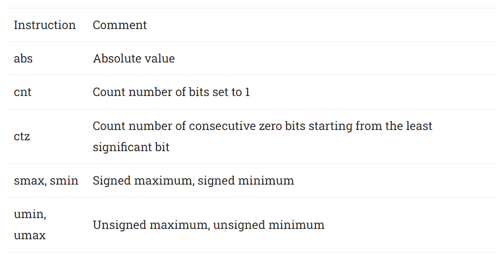
Arm’s NEON extension could already do some of these things (like absolute value), but required the programmer to load the value into vector registers. CSSC brings those functions to the scalar integer side.
Different Code Generation Options
Ampere 1B has two extra “features” enabled for code generation. FeatureEnableSelectOptimize tells LLVM to try using conditional selects whenever possible. Then, FeaturePredictableSelectIsExpensive tells LLVM to not prefer that optimization if the alternative is a well predicted branch.
Conditional selects or conditional moves can be used to handle an if (a) { b = c } else { b = d } sequence without using a branch. Avoiding a branch can be favorable if it’s mispredicted often. Intel’s Pentium 4 notably could benefit from such optimizations, because it had an exceptionally high branch mispredict penalty.
However, modern CPUs are much better at branch prediction and recover faster from mispredicts. Ampere decided that a correctly predicted branch should be considered more performant than using a conditional select. That’s probably the correct decision for all decently designed cores from the past decade, so seeing it isn’t a surprise. Ampere One in particular has a relatively short 10 stage pipeline, so it can detect mispredicts early. Likely, it can do fast mispredict recovery like other modern cores by restoring a renamer checkpoint. Thus preferring to avoid conditional selects if a branch is likely to be correctly predicted most of the time is definitely the right move for Ampere One.
Summarizing Ampere 1B
Ampere 1B is a straightforward evolution of the Ampere One architecture, and fixes Ampere One’s vector/FP latency issues. It also improves memory load latency and increases ROB size. All of those changes together should give Ampere 1B a noticeable IPC gain over Ampere One. Finally, it gets expanded ISA extension support.
While Ampere 1B is a derivative of Ampere One, the changes are big enough that I feel it can be treated as a separate generation. Perhaps Ampere 1.5 would be a better name for the architecture.
Final Words
Ampere Computing wants to follow up on Ampere Altra’s success in the cloud market. Their Ampere One CPUs appear to be even more density optimized than the Neoverse N1 cores used in Altra, and look to continue the company’s success. LLVM commits can’t tell the whole story about the cores, but they do shed light on the company’s strategy. Ampere One and its successors have relatively small out of order execution engines compared even to Arm’s 7-series Cortex designs. They’re especially light on FP/vector performance, and avoid spending area on features like SVE that won’t pay off in the moment.
SVE’s Rocky Adoption Path
Scalable Vector Extensions, or SVE, modernizes aarch64’s vector capabilities. It adds mask registers and allows flexible vector widths up to 2048 bits. But Ampere’s strategy likely causes Arm Ltd some headaches. Every ISA extension faces a chicken and egg problem where software developers are reluctant to dump time into using a new ISA extension until a critical mass of users stand to benefit. Meanwhile, consumers may be unwilling to pay extra for a CPU that supports a certain ISA extension unless they’re using software that benefits from it.

Arm Ltd seems to be trying to address that critical mass problem within the next few years by rolling SVE into consumers’ regular upgrade cycles. They’ve made SVE part of the armv9 standard. In their core designs, Arm has gone through the trouble of making sure all their mobile cores support SVE. Even the Cortex A510 supports SVE, mitigating costs with a shared FPU setup. If everyone used Arm designs or rolled their own SVE(2) implementations, you wouldn’t be crazy to expect a significant SVE install base by 2035 or so.
Unfortunately for those plans, Ampere Computing is a significant force in the Arm server market. Ampere One’s lack of SVE support means there’s gonna be a lot of current-generation Arm server CPUs without SVE. Worse, Qualcomm in their infinite wisdom has decided not to enable SVE support even though their newer Snapdragon SoCs use Arm Ltd’s SVE capable cores. Like Ampere, Qualcomm is a huge force in the the mobile aarch64 CPU market. Thus NEON/ASIMD will likely remain the standard aarch64 vector extension to target for years to come.
Ampere’s Density Goals
Assuming Ampere Computing does a good job of meeting their density goals, the next question is how far they can take that strategy. Getting high performance via a larger number of weaker cores is nothing new, but taking advantage of high core count is always difficult. Amdahl’s Law applies when an application can only be partially parallelized. Even the multithreaded part of a program may have its gains capped by a limited parallelization factor. Finally, code with enough parallelism may run into memory bandwidth bottlenecks. Ampere One’s 8-channel DDR5 interface is impressive, but AMD has seen fit to give 96 core Genoa and 128 core Bergamo parts a 12-channel DDR5 setup. AMD’s Zen 4 parts have more cache per core too, which can help reduce memory bandwidth demands.
Some of those drawbacks may be mitigated in the cloud computing market that Ampere targets. There, cloud providers typically allocate computing resources to VMs at the core granularity. More cores mean more VMs and thus more customers per chip, assuming the individual cores are powerful enough to meet customer needs. Yet this approach isn’t problem free either. Each VM needs enough memory to run its isolated operating system along with whatever applications the customer needs.
4 GB per core might be a good baseline. That’s what Google Cloud gives general purpose T2A Ampere Altra instances. A dual core VM would therefore have a comfortable 8 GB of memory, which Apple for example believes should be enough for daily use. To support that, an Ampere One chip would need 768 GB of DDR5 installed, not counting overhead for the hypervisor and management functions. A 1DPC (one DIMM per channel) setup would require 128 GB memory sticks. Newegg is happy to sell these at $1300 per stick. That’s $7800 for 768 GB of memory, or $10,400 for a balanced configuration that maximizes bandwidth. I couldn’t find pricing figures for an Ampere One chip, but for perspective, $10,400 is about as much as a 128 core AMD Bergamo chip.
Meeting the same 4 GB per core baseline with a 96 core Genoa chip would require 384 GB of memory, which can be achieved with much cheaper 64 GB DIMMs. Newegg sells those for about $230 each. Thus the cost benefit of packing more cores into each server may be offset by the insane cost of high capacity DIMMs.

Finally, reliability and redundancy requirements can cap benefits from higher density chips. Using fewer servers means the same amount of work is sitting on top of fewer server-wide components like network cards, motherboards, and power supplies. If a hypothetical rack of six servers is reduced to four thanks to higher core count CPUs, a failure that forces one server offline would reduce the rack’s capacity by 25% instead of a more manageable 16.6%. Just as consolidating data from several smaller hard drives onto a 20 TB one is a bit scary because everything’s lost if that drive crashes, consolidating servers can increase risk for a company.
I don’t normally care about business matters, but I’ll be interested in seeing how large the density optimized market is. Even a smaller core like Ampere One requires tons of engineering effort to properly optimize and validate. The size of Ampere One’s target market may affect how much engineering power the company can put behind its in-house core designs. That in turn will determine how ambitious the company can be when evolving its Ampere One architecture.
What’s Next?
Google announced C3A Ampere One instances in August of last year. C3D Genoa VMs from the same announcement became generally available just a couple months later. We’re in the middle of February this year and Google is still not confident enough to make Ampere One instances generally available.
Google’s announcement further reveals that Ampere One instances will be capped to 80 vCPUs. It’s a strange limitation because Google’s C3D Genoa instances can scale to 360 vCPUs (180 physical cores), and prior generation N2D Milan VMs can scale to 224 vCPUs (112 physical cores). Perhaps Google has chosen not to buy Ampere One’s top end 192 core chips, which brings its density advantage into question. If so, I wonder if Google wasn’t able to get VMs to span sockets on Ampere One.
Whatever the case, Ampere Computing will have a good looking future if Ampere One is as successful as its predecessor, Ampere Altra. On that note, I hope Google is able to make some kind of Ampere One instance generally available before Valve does the same for a Steam Deck successor. I’ve heard rumors they’ll do that before 2069.