
Inside Kepler, Nvidia’s Strong Start on 28 nm

Nvidia’s Fermi architecture was ambitious and innovative, offering advances in GPU compute along with features like high tessellation performance. However Terascale 2’s more traditional approach delivered better power efficiency. Fermi’s GTX 500 series refresh narrowed the efficiency gap, but then AMD hit back with the GCN architecture on 28 nm. In developing their first 28 nm GPU architecture, Nvidia threw away most of the Fermi playbook and focused hard on power efficiency.

As part of this effort, Kepler trades some of Fermi’s compute credentials for a more balanced approach. Nvidia had high hopes for GPU compute, but consumers didn’t end up using GPUs to provide additional floating point throughput in everyday applications. GPUs were still primarily for gaming, and had to be good at it.
I waited for a long time for a site like Real World Tech to deep dive Kepler’s architecture, but it never happened. I guess I’ll do it myself.

Kepler has a few variations, and I’ll be focusing on GK104 and GK210.
I’ll occasionally make references to AMD’s GCN and Nvidia’s prior generation Fermi architecture for comparisons.
System Level
Kepler is built from SMX-es, or Next Generation Streaming Multiprocessors. The entire GPU gets a shared L2 cache as with Fermi, although some Kepler SKUs get doubled L2 cache capacity.

A GDDR5 setup provides high DRAM bandwidth to the GPU. Fermi also used GDDR5, but Kepler’s GDDR5 controllers can handle higher GDDR5 clocks for increased bandwidth. A PCIe 3.0 connection links Kepler to the host system, and provides twice as much bandwidth compared to Fermi’s PCIe 2.0 setup.
Kepler SMX Overview
Kepler’s SMX is distantly related to Fermi’s SMs, but is much larger and prioritizes power efficiency. Fermi ran the execution units at twice the GPU core clock to maximize compute power within area constraints, but that resulted in high power consumption. Kepler drops the hot clock in favor of more execution units, using more die area to achieve better performance per watt. Therefore 96 “cuda cores” on a GK104 chip are equivalent to 48 on a GF104 chip running at the same clocks.

To claw back some area efficiency, Nvidia packs more execution power into the SMX. Doing so reduces instances of shared resources like caches, scratchpad storage, and off-SMX interfaces. A SMX thus ends looking like a doubled-up Fermi SM. It’s capable of completing 192 FP32 operations per cycle, making it a giant basic building block.
SMX Frontend
A SMX feeds its four scheduler partitions with a 8 KB instruction cache. Each scheduler partition, or SMSP (SM sub-partition) can exploit thread-level parallelism by tracking up to 16 threads. Nvidia calls these threads warps, since each instruction generally operates on a 32-wide vector of 32-bit elements. Every cycle, the scheduler can select a thread and issue up to two instructions from it to the execution units. Unlike Fermi’s scheduler, Kepler uses static software assisted scheduling.
Static Scheduling
Fermi’s instruction set looks a bit like ARM or x86. The instructions say what to do, but not how fast to do them. That job falls to Fermi’s hardware, which uses a scoreboard to track register state and stall instructions until their input registers are ready.

Fermi could dual issue FMA instructions and a FMA instruction has three inputs. The register scoreboard would therefore need at least six read ports and two write ports. Covering the register file would require 1024 entries, since a Fermi SM has a 1024 entry register file.
Kepler does away with this structure by taking advantage of fixed execution latencies. A FMA operation will always produce a result in 9 cycles, and the compiler knows this. The hazard detection process for these fixed latency operations can be avoided if the hardware can be told to wait for a fixed number of cycles. To do this, Kepler adds scheduling info to its instruction set. Every seven instructions is preceded by a 64-bit control word.

Within the control word, one byte identifies it as control information (not a regular instruction), while the other seven bytes contain scheduling info for each of the subsequent instructions. The control byte can tell Kepler to stall the thread for a number of cycles, after which register inputs will be ready. Hardware unconditionally trusts the scheduling info. If you set the control code yourself and don’t stall for enough cycles, you’ll get the wrong results.
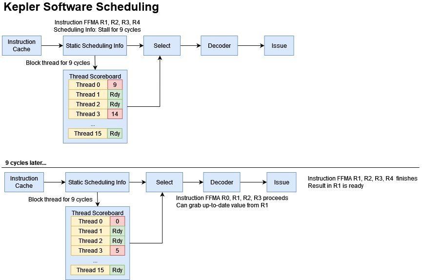
Besides stall cycles, Kepler’s control codes can tell the scheduler to dual issue a pair of instructions. Fermi’s dual issue capability required the hardware to check adjacent instructions for dependencies, but Kepler gets rid of that.
Thus Nvidia has replaced Fermi’s large, multi-ported register scoreboard with a simpler structure that tracks readiness on a per-thread basis. Each scheduler partition can only track 16 threads, so the structure can be small. Because the scheduler will only select one thread for execution per cycle, the thread scoreboard only has to provide one output and accept one write per cycle.
Execution Units
The instruction(s) selected by the scheduler have their operands read from the register file. Consumer Kepler variants have a 64 KB register file for each scheduler partition, letting it track state for up to 512 32-wide vectors. GK210 has twice as much register file capacity, likely to improve occupancy with FP64 workloads. The register file is built with four single-ported banks and therefore can only provide four operands per cycle. Dual issuing FMA instructions would require up to six register inputs. Kepler therefore has an operand collector capable of caching recently read register values.
Once operands are ready, instructions are sent to two execution ports. Each can handle a 32-wide vector per cycle, but the second port is shared by two scheduler partitions. Integer operations are handled by the first non-shared port, and thus execute at 2/3 of FP32 rate. Special function operations like reciprocals and inverse square roots execute at quarter of the integer rate.

Common INT32 and FP32 operations execute with 9 cycle latency5, making Kepler more prone to data hazard stalls than newer GPU architectures. But if execution dependencies are rare, Kepler can get through individual kernel invocations with blazing speed. Like RDNA, it can execute instructions from the same thread on back-to-back cycles. Combine that with dual issue capability, and Kepler’s per-thread, per-cycle throughput is second only to AMD’s RDNA 3.
Kepler has less execution throughput compared to AMD’s competing GCN GPUs. Nvidia especially de-prioritized FP64 execution hardware on consumer SKUs. Games don’t use FP64 because graphics rendering doesn’t require high accuracy. Having extra FP64 units would be a waste of die area.

Kepler products focused for datacenter and HPC like the GK210-based Tesla K80 did offer high FP64 throughput. However, taking advantage of that FP64 capability comes at a substantial power cost, even at low clocks. The Tesla K80 is nominally capable of 824 MHz, but clocks drop as low as 744 MHz under sustained FP64 load. As temperatures rise, leakage power gets worse and the card clocks down to stay within power limits.

Where Kepler shines is bringing more execution power to bear when faced with small kernels. A SMX sub partition can nominally issue one instruction per clock and occasionally dual issue. A GCN SIMD can only issue one instruction every four clocks.
Cache and Memory Access
A Kepler SMX has several types of private caches for different memory spaces. Global memory is the GPU’s main memory space and acts like CPU memory. It’s backed by VRAM, and writes are visible across the GPU. Accesses to global memory can be cached by L1. Texture memory is read-only and backed by separate caches on Kepler. Nvidia’s GK110/GK210 whitepaper refers to the texture cache as a “read-only data cache”.

Constant memory is meant for read-only variables, and is specified via the “__constant” qualifier in OpenCL. Kepler’s SMX has a two-level constant cache.
Finally, each OpenCL workgroup or CUDA thread block can allocate scratchpad memory. OpenCL calls this local memory, while CUDA calls it shared memory.
Global Memory
Like Fermi, L1 cache and shared memory (a software managed scratchpad) are dynamically allocated out of a 64 KB block of storage. In addition to supporting Fermi’s 16+48 KB split, Kepler adds an evenly split 32+32 KB option.

GK210 Kepler doubles L1/shared memory storage to 128 KB, potentially helping occupancy with programs that allocate a lot of scratchpad storage. L1 cache capacity stays capped at 48 KB, suggesting Nvidia didn’t increase the tag array size. Latency to the L1 data cache remains constant regardless of the L1/scratchpad storage split.

Compared to GF114 Fermi, GK210 Kepler has somewhat higher cache and memory latency. The Tesla K80 is a rather low clocked Kepler product and has a core clock similar to the GTX 560 Ti’s (824 vs 823 MHz), which likely accounts for the lack of improvement.
Frustratingly, OpenCL and CUDA kernels can’t access GK104’s L1 data cache. I tried both OpenCL and CUDA with the opt-in compiler flags set. Somehow it works with Vulkan, so I’m using Nemes’ Vulkan microbenchmark to compare with AMD’s HD 7950.

Nvidia’s GTX 680 has better vector access latency throughout the memory hierarchy. AMD enjoys better latency if it can leverage the scalar memory path, which only works for values known to be constant across a 64-wide wavefront. Nvidia’s driver in its infinite wisdom has chosen the smallest L1 data cache allocation for Vulkan even though the kernel doesn’t use scratchpad memory. Otherwise, Nvidia could have a L1D capacity and speed advantage over AMD.
Texture Caching
Nvidia’s GK110/210 whitepaper2 says each SMX has 48 KB of texture cache. However, my testing only sees 12 KB. Größler’s thesis3 shows similar results. An investigation by Xinxin Mei and Xiaowen Chu suggests both Kepler and Fermi use a 12 KB, 96-way set associative texture cache. This discrepancy is because Kepler appears to have a private texture cache for each scheduler partition.

I created disjoint pointer chasing chains within the test array and spawned multiple sets of 32 threads within the same workgroup. Nvidia’s compiler appears to assign adjacent OpenCL threads to the same wave (vector), so I had each set of 32 threads follow the same chain to avoid divergent memory accesses. Keeping the test within one workgroup meant all waves would be assigned to the same SMX. Spawning two waves shows low latency over 24 KB, and spawning four shows the 48 KB of texture cache capacity claimed by Nvidia’s whitepaper.
Thus, I disagree with Mei and Chu’s conclusion that each Kepler SM has 12 KB of texture cache per SM(X). Rather, I think it has 12 KB of texture cache per SMX scheduler partition, giving each SMX four 12 KB texture caches and 48 KB of total texture cache capacity.

Compared to GCN, Kepler enjoys lower latency access for image1d_buffer_t accesses. GCN’s vector cache doubles as a texture cache, so we’re comparing Kepler’s texture cache to GCN’s vector cache accessed (probably) through the TMUs. Latencies are closer this time, likely because array address calculations are handled by the TMUs, and they’re faster than doing the equivalent shift + add sequence through the vector ALUs.

Texture cache misses go to L2. Larger Kepler chips like GK210 enjoy larger L2 capacity, but latency is higher compared to consumer GK104 and GK107 chips. Part of this can be attributed to the Tesla K80’s lower 824 MHz clock speed. The GTX 680 and GTX 650 run at 1058 MHz.
Constant Memory
To speed up access to variables constant across a vector (warp/wave), Kepler has a small but fast 2 KB constant cache. A mid-level 32 KB constant cache helps cache more constants. Kepler supports up to 64 KB of constants.
Compared to Fermi, Kepler shrinks the constant cache from 4 KB to 2 KB. Latency regresses as well, rising to 46.9 ns compared to Fermi’s 30.58 ns. Kepler and Fermi both have a 32 KB mid-level constant cache that’s probably private to a SM(X). Latency is slightly higher on Kepler, suggesting Nvidia has de-prioritized constant caching. Perhaps constant memory access was already fast enough on Fermi and pipelines could be lengthened to allow higher clocks at lower voltage.

AMD does not have a separate constant cache hierarchy. Instead, the 16 KB scalar cache handles both constant memory and scalar global memory accesses. GCN therefore enjoys more first level caching capacity for constant memory, and a latency advantage out to 16 KB. Past that, accesses spill into L2.
Strangely, Fermi’s compiler can optimize scalar accesses to use the constant cache, making it play a role similar to AMD’s scalar cache. This optimization is gone with Kepler, and the constant cache hierarchy can only be accessed if memory is marked with the “__constant” qualifier in OpenCL.
Local Memory
Unlike other memory types, local memory is not backed by DRAM. It’s a small software managed scratchpad local to a group of threads running in the same SMX. Nvidia confusingly calls this “Shared Memory” even though it’s less shared than global memory. AMD calls their equivalent the “Local Data Share”.

Local Memory provides better latency than L1 cache accesses even though Kepler allocates both out of the same pool of storage. That’s because local memory is directly addressed and doesn’t require checking cache tags. On Kepler, local memory offers the lowest latency storage (besides registers of course). It’s a bit faster than Fermi and much faster than competing GCN GPUs. On the HD 7950, pointer chasing in the LDS is barely faster than doing so within the vector cache. The R9 390 improves, but is still far off from Kepler.
Atomics
Atomic operations help pass values between threads running on a GPU. Kepler features improvements to atomic handling, with the L2 getting increased bandwidth for atomics compared to Fermi6. Nvidia has evidently improved latency for atomic operations too. When using atomics on global memory, Kepler offers far lower latency than Fermi and edges out AMD’s GCN architecture.

We can also do atomic operations on local memory. Doing so passes values between two threads running on the same SMX, and should result in lower latency. AMD benefits nicely if atomic operations are kept within a compute unit, but Nvidia does not. Fermi saw the same behavior.

Bandwidth
For a 2012 GPU, Kepler has good latency characteristics. However, graphics rendering is inherently bandwidth hungry. Kepler is outclassed by AMD’s GCN throughout the global memory hierarchy.

Shared caches are particularly interesting because they have serve a lot of clients and meet their bandwidth demands. Nvidia has doubled per-cycle L2 cache throughput on Kepler, giving GK104 512 bytes per cycle of theoretical L2 bandwidth6. Assuming Nvidia is using one L2 slice per 32-bit GDDR5 channel, GK104’s L2 cache would consist of eight 64 KB slices, each capable of 64 bytes per cycle of bandwidth. At 1058 MHz, the L2 cache should deliver 541 GB/s of total bandwidth. I don’t see anything near that.

Varying workgroup count doesn’t create much of a difference in measured bandwidth. I expect AMD’s HD 7950 to have more L2 bandwidth because L2 slices are typically tied to DRAM controllers. Tahiti’s wider DRAM bus would imply more L2 slices and more bandwidth. But more than a 2x difference in measured bandwidth is unexpected. Still, GK104’s L2 offers twice as much measured bandwidth as DRAM access.

GK210 Kepler (Tesla K80) features a larger 1536 KB L2 cache, likely with twelve 128 KB slices. Since GK210 has a 384-bit memory bus like AMD’s Tahiti, bandwidth should be more comparable. However, GK210 still falls short. Running two workgroups in each SMX slightly improves bandwidth from 338 to 360 GB/s, but providing even more parallelism doesn’t improve results further. Zhe Jia et al7 achieved a similar 339 GB/s on a Tesla K80 using CUDA with PTX, so I’m not crazy.

Kepler has less VRAM bandwidth than GCN cards, thanks to smaller memory buses. Vulkan microbenchmarking achieved 142 GB/s from the GTX 680’s VRAM setup, compared to 192 GB/s theoretical. The same test got 204 GB/s on the HD 7950, out of 240 GB/s theoretical. This difference persists as we move to larger chips. GK210 gets a 384-bit memory bus, but Hawaii’s 512-bit bus keeps it ahead.
Some Light Benchmarking
Various reviewers have covered Kepler’s gaming performance when the card first launched. Anandtech’s review is a good example, and I highly encourage going over that to get an idea of where Kepler stood against GCN around 2012. That said, I think it’ll be fun to throw a few modern compute workloads at the card and see what happens.

VkFFT implements Fast Fourier Transforms using Vulkan. Nvidia’s GTX 680 couldn’t finish the benchmark, so I’m presenting results from the sub-tests that did complete.

AMD’s GCN architecture pulls ahead in VkFFT, often by a large margin. VkFFT is not cache friendly and heavily loads the VRAM subsystem. The creator of VkFFT, Dmitrii Tolmachev, collected a profile on the RTX 3070 mobile showing 93% of memory throughput and 30% of compute throughput used.
I also profiled the benchmark on my RX 6900 XT and saw occupancy limited by local memory (LDS) capacity. Kepler’s unified 64 KB L1/Shared Memory setup may work against it compared to AMD’s separate 64 + 16 KB LDS and L1 vector cache configuration.
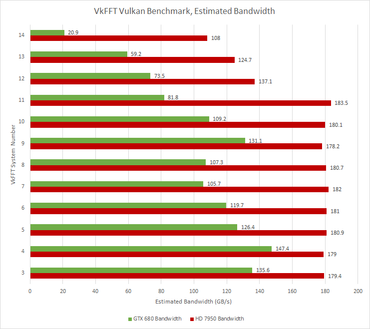
VkFFT also prints out estimated memory bandwidth utilization. The figures suggest both cards are memory bandwidth bound, with AMD’s GCN-based HD 7950 pulling ahead thanks to its wider memory bus.
FluidX3D uses the lattice Boltzmann method to simulate fluid behavior. It features special optimizations that lets it use FP32 and still deliver accurate results in “all but extreme edge cases”. I’m using FluidX3D’s built-in benchmark.

FluidX3D can demand a lot of memory bandwidth, but somehow the situation reverses compared to VkFFT. AMD’s HD 7950 now falls behind despite a theoretical advantage in both FP32 compute and VRAM bandwidth. Interestingly, GCN’s performance improves dramatically as we move to Hawaii. The R9 390 is able to beat out the Tesla K80.
Upscayl uses machine learning models to upscale images. I’m using the default Real-ESRGAN model to double a photo’s resolution. Upscayl doesn’t feature a benchmark mode, so I’m timing runs with a stopwatch.

Kepler compares badly to the HD 7950, and takes several times longer to process the image.
Final Words
GPU designers have to achieve high performance while balancing area and power consumption. Kepler re-balances area and power priorities compared to Fermi by focusing more on power efficiency. Compared to AMD’s GCN architecture, Kepler falls behind on headline specifications like compute throughput and memory bandwidth. To make up for this, Kepler makes its compute throughput easier to utilize. A single thread can access more execution resources, and vector memory accesses enjoy lower latency. The result is a high performance and power efficient architecture that put Nvidia on solid ground as the 28 nm era started. After its GTX 600 series debut, Kepler went on to serve in the GTX 700 generation.
Of course they compared to Kepler. Everyone compares to Kepler
Bill Dally at Hot Chips 2023 talking about the first TPU paper
Despite Kepler’s focus on better gaming performance, compute variants of the architecture saw success thanks to Nvidia’s strong software ecosystem. Tesla K20x GPUs secured multiple supercomputer wins, including Oak Ridge National Laboratory’s Titan.

Besides being a solid product, Kepler served as a proving ground for techniques that would feature in subsequent Nvidia architectures. Kepler’s static scheduling scheme was successful enough to be used in every Nvidia generation afterward. The control code format would change to allow more flexibility and hand even more responsibility over to the compiler, but the core strategy remained. Kepler’s division of the basic SM building block into four scheduler partitions was also carried forward.

From the consumer point of view, Kepler was part of a series of Nvidia generations that each provided compelling upgrade options over the previous generation. Fermi, Kepler, Maxwell, and Pascal delivered such an improvement in performance, value, and power efficiency that used card prices would crater as new ones became available. It’s a stark contrast to today’s GPU market, where a last-generation RX 6700 XT still commands midrange prices more than two years after its release. I can only hope that the GPU market moves back in that direction.
If you like our articles and journalism, and you want to support us in our endeavors, then consider heading over to our Patreon or our PayPal if you want to toss a few bucks our way. If you would like to talk with the Chips and Cheese staff and the people behind the scenes, then consider joining our Discord.
References
Xiuxia Zhang et al, “Understanding the GPU Microarchitecture to Achieve Bare-Metal Performance Tuning”
Nvidia’s Next Generation CUDA Compute Architecture: Kepler GK110/210
Dominik Größler, “Capturing the Memory Topology of GPUs“
Xinxin Mei, Xiaowen Chu, “Dissecting GPU Memory Hierarchy through Microbenchmarking“
Yehia Arfa et al, “Low Overhead Instruction Latency Characterization for NVIDIA GPGPUs”
Zhe Jia et al, “Dissecting the NVidia Turing T4 GPU via Microbenchmarking”