
Ivy Bridge’s Gen7 Graphics: Intel’s Modern iGPU Push

Intel has maintained an integrated graphics effort for a long time. The company’s integrated GPUs were not expected to do much beyond driving a display and offloading video decode. You could run games on them, but would probably be looking at poor framerates even at low quality and low resolutions. Ivy Bridge didn’t aim to change that fundamental picture, but it does represent a shift in Intel’s strategy towards creating a more flexible, programmable GPU.
In that sense, Ivy Bridge’s graphics architecture represents a turning point in Intel’s graphics strategy, introducing a solid foundation for Intel’s future graphics efforts. While Intel would not attempt to create a truly high performance graphics solution until nearly a decade later, Ivy Bridge graphics (also known as Gen 7) would pave the way for that effort.
I highly suggest reading Real World Technologies’s excellent article on Ivy Bridge’s graphics architecture, because it provides a lot of contemporary insight into the technology. My goal here is to supplement RWT’s analysis, instead of writing a full length article.
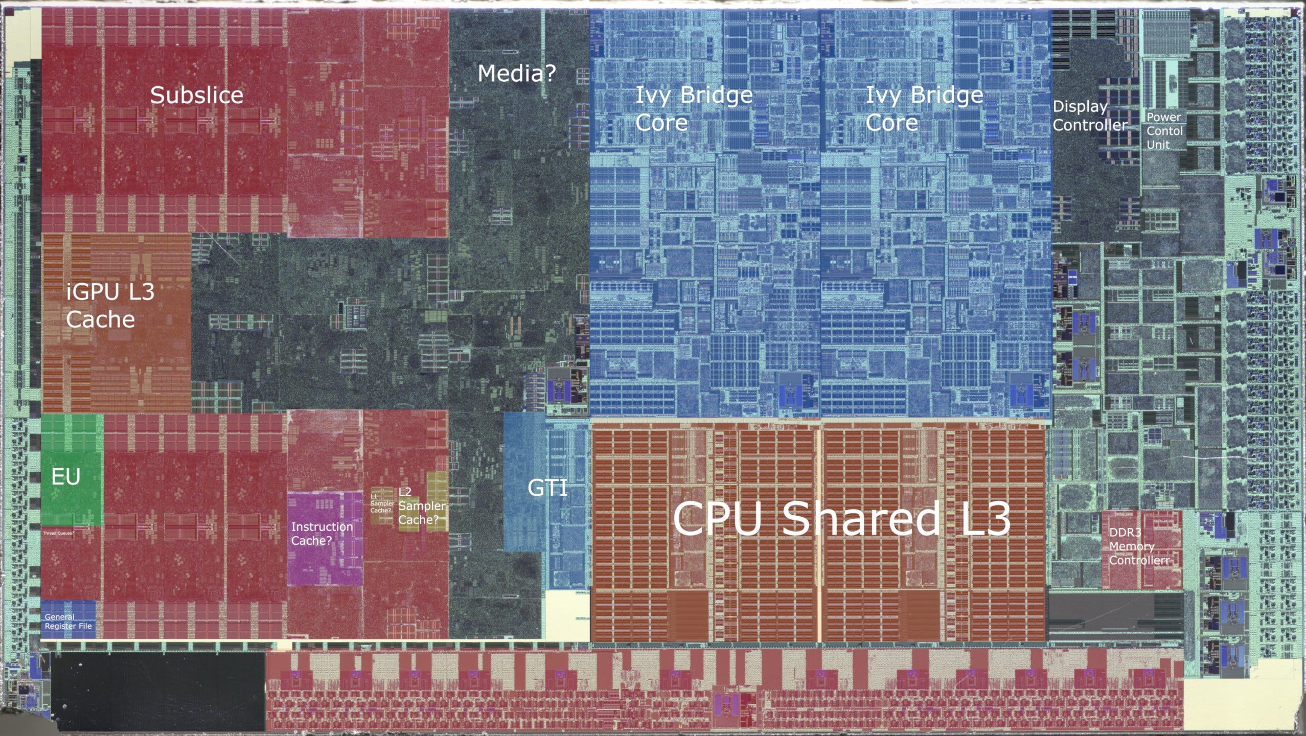
System Level
A Gen 7 iGPU is built from execution units (EUs), organized into subslices. A subslice contains private caches, texture units, and an interface to the rest of the GPU. In that sense, a subslice is most similar to AMD’s Compute Units (CUs) or Nvidia’s Streaming Multiprocessors (SMs). CUs and SMs form the basic building block of AMD and Nvidia’s GPUs, and those companies scale to very large GPUs. Gen 7 isn’t like that. Instead, it lets Intel tune GPU size in very small increments. Intel can adjust the EU count in each subslice, giving them a lot of flexibility to adjust very small GPUs. The equivalent would be adjusting the SIMD count within an AMD CU, or SMSP count within a Nvidia SM.

Gen 7’s shader array is backed by a GPU-wide cache, which Intel confusingly calls L3 (because each subslice has two levels of private texture caches). Unlike discrete GPUs, the iGPU interfaces to the host by being another agent on the CPU’s ring bus. From there, GPU memory accesses get treated a lot like regular CPU requests.
The Gen 7 Execution Unit
Gen 7’s EU is the smallest unit of compute execution. Instructions are fed in from a subslice-shared instruction cache. Then they enter a set of per-wave instruction queues, where they can be selected for execution. Every cycle, Gen 7’s scheduler can select a pair of waves to issue every cycle, to a pair of execution units. Both execution units support the most common operations, so Intel expects dual issue to be a regular mode of operation, rather than occasionally taking load off a primary compute pipeline as is done in Nvidia’s Maxwell and Pascal.

Once a pair of waves is selected for execution, their operands are fetched from the register files by the operand collector. This operand collector supports extremely sophisticated register file addressing. Most GPUs have instructions that directly address the vector register file via a register index. Intel is special and lets you use registers to address your registers. Gen 7’s vector register file supports register-indirect addressing via set of separate address registers. These address registers are 16 bits wide, and each wave can access eight of them, allowing register indirect register addressing for wave8 mode (but not wave16). Variable wave sizes are also supported at the instruction granularity. Each instruction can specify how many elements it wants to operate on and a register file region to get that data from, though terms and conditions may apply.

Unlike Nvidia and AMD, vector registers are not dynamically allocated. Each wave gets 128 registers, and the scheduler can track up to eight active waves. Using fewer registers does not allow increased occupancy, and there’s no way to use more registers per thread in exchange for lower occupancy.
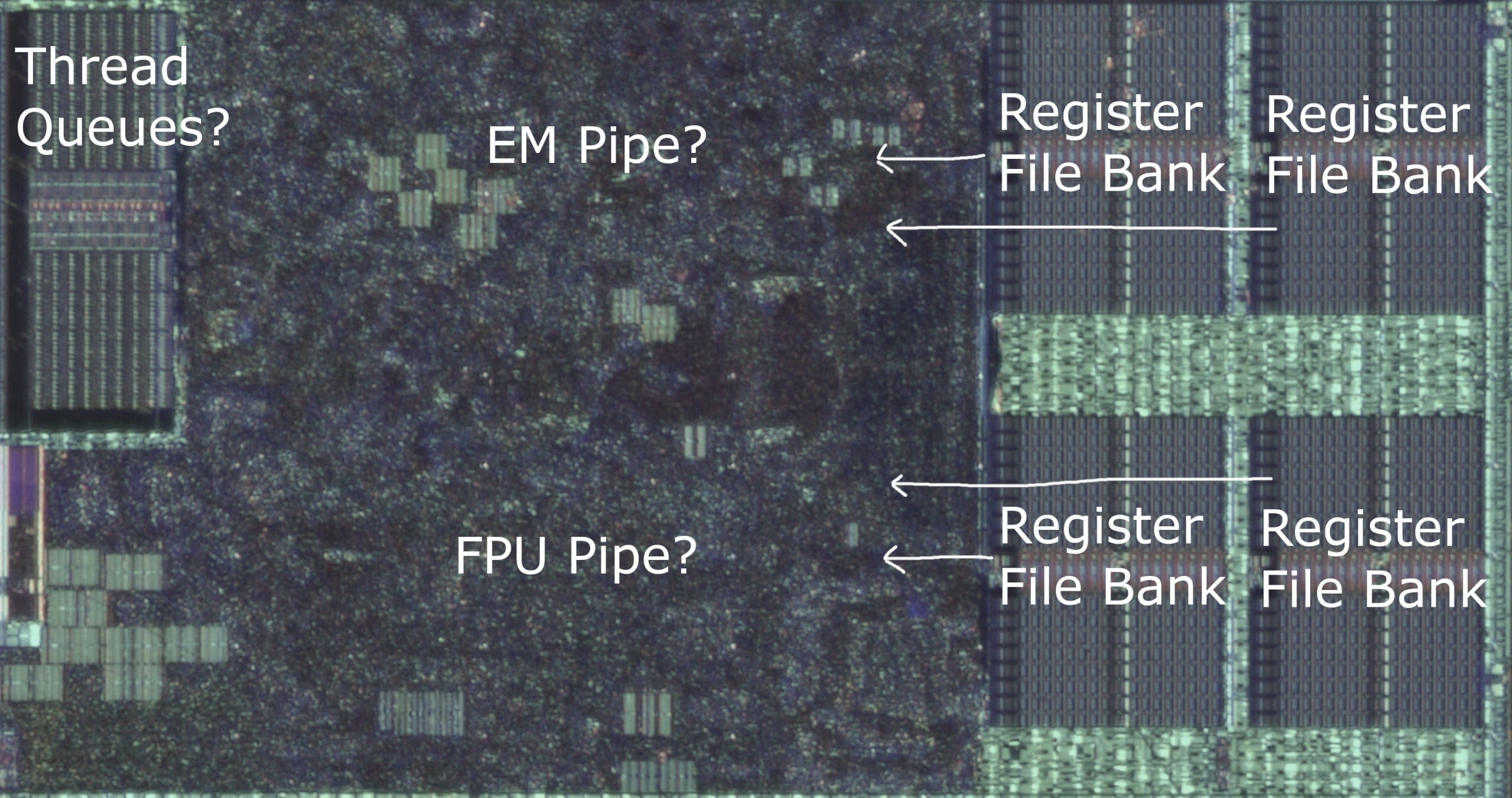
Once instructions have finished getting their operands, they get to Gen 7’s two execution pipes. For legacy reasons, Intel names these the “FPU Pipe” and “EM Pipe”. EM stands for Extended Math, because that pipe originally only handled complex math operations like reciprocals and inverse square roots. Gen 7 augments that pipe so it can handle floating point additions and fused multiply-adds. In any case, Intel has a lot of execution resources on hand for special operations, and comparatively less for integer operations. INT32 instructions can only use the first pipe, and thus execute at half rate compared to FP32 instructions.

The HD 4000 is roughly comparable to Nvidia’s Quadro 600, which is a small implementation of Nvidia’s Fermi architecture. The Quadro 600 is often used to drive displays in systems without an integrated GPU, or to supplement an iGPU to provide more display outputs. Throughput is similar for basic FP32 operations, but Gen 7 has a large lead in special operations, as well as INT16 and INT8 throughput. These architectures are from a time when low precision throughput wasn’t prioritized, but it’s interesting to see Gen 7 doing a passable job there. Meanwhile, Nvidia has stronger integer multiplication performance, and can do 64-bit integer additions with less of a penalty.
Memory Access
Each Gen 7 subslice is responsible for feeding a gaggle of EUs, and has two-level sampler cache setup to help with that. Again, this contrasts with AMD and Nvidia designs, where there’s just a single level of texture caches in each basic GPU building block.

Instead of using direct memory access instructions, EUs use a ‘send’ instruction to send messages to subslice-level components. For example, global or local memory would be accessed by sending a message to the subslice’s data port. Texture accesses would similarly involve sending a message to the subslice’s sampler. Intel’s EUs are likely quite decoupled from subslice shared logic, while AMD’s SIMDs or Nvidia’s SMSPs are probably tightly integrated with CU or SM level hardware. This could be part of what enables GPU sizing at the EU level.
We can test the sampler caches with buffer accesses, via OpenCL’s image1d_buffer_t type. This type doesn’t support any sampler options, so the sampler simply has to act like a plain AGU and directly retrieve data from memory. Even with such simple accesses, hitting the L1 sampler cache takes an agonizing 141 ns. Latency slightly increases to 145 ns as we get into the L2 sampler cache.

Global memory accesses from compute kernels bypass the samplers and hit the iGPU-wide L3, likely because sampler accesses incur such devastatingly high latency even with sampler options off. The L3 can be accessed with just above 87 ns of latency. Nvidia’s Fermi enjoys slightly lower latency for small test sizes, but can’t match Intel’s combination of low latency and high caching capacity.

Gen 7’s L3 should have 256 KB of capacity, but some part of it will always be reserved for fixed function hardware. I’m testing Gen 7 on a Surface Pro. Because the iGPU is always connected to the built in display, there’s less L3 capacity available for GPU compute when compared to a desktop where the iGPU can be enabled without a display attached. Still, 128 KB of user-visible caching capacity compares quite favorably to small GPUs. Nvidia’s Quadro 600 only has 128 KB of last level cache, and Fermi’s L2 takes far longer to access.
VRAM latency is very well controlled on Intel’s iGPU. Both the Core i5-3317U and Nvidia’s Quadro 600 use a dual channel DDR3-1600 memory setup, but Fermi’s memory latency is far worse. Intel likely benefits from a very latency optimized memory controller, since CPUs are very latency sensitive.
Local Memory
GPUs typically have fast scratchpad memory that offers an alternative to the slower global memory hierarchy. With OpenCL, this memory type is called local memory. AMD and Nvidia GPUs back local memory with fast building-block-private blocks of SRAM. AMD calls this the Local Data Share (LDS), while Nvidia calls it Shared Memory. Gen 7 does not do this. Local memory is allocated out of the GPU’s L3 cache, so latency isn’t the best. It’s a touch better than accessing the L3 as a regular cache, because there’s no need for tag or status checks.
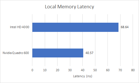
Nvidia also has a block of memory serve double duty as cache and local memory. But that memory is private to a SM and can be accessed quickly. Fermi therefore enjoys far better local memory latency.
Atomics
Atomics can be used to synchronize different threads running on the GPU, and exchange values between threads. Here, we’re testing OpenCL’s atomic_cmpxchg function, on both global and local memory. Typically, a GPU will see far lower thread-to-thread latency when testing with local memory, since that’s roughly analogous to passing data between sibling threads on a SMT-enabled CPU. However, Gen 7’s local memory isn’t local to a subslice, so we don’t see a particularly large latency difference between local and global atomics.

Nvidia’s Fermi is much slower at handling atomics. Atomics on local memory take much longer than uncontested accesses, suggesting the SMs don’t have particularly fast synchronization hardware. There’s also a huge penalty for going to global memory, even though there are only two SMs on the Quadro 600.
Bandwidth
High performance GPUs tend to be quite bandwidth hungry, and can pull hundreds of gigabytes per second from caches and VRAM to feed their giant shader arrays. Gen 7 is not designed for that. Its GPU-level L3 can still deliver a decent amount of bandwidth though, and compares favorably to Nvidia’s tiny Fermi.

As with any integrated GPU, Gen 7 shares a memory controller with the CPU. In this case, it’s a dual channel DDR3 controller capable of providing 25.6 GB/s. Nvidia’s Quadro 600 has exactly the same, so its only advantage to being a discrete GPU is that it won’t have to fight with the CPU over memory bandwidth.

Bandwidth is low, but that’s expected for a low end GPU of the era. There’s not a lot of compute power to feed on either GPU, so bandwidth bottlenecks shouldn’t be a huge issue.
Link Bandwidth
Integrated GPUs tend to have an advantage when moving data between CPU and GPU memory pools, because the memory pools are physically the same. Intel’s architecture in particular lets the CPU and GPU pass data through the L3 cache. Future Intel iGPUs could get massive bandwidth with small copies between the CPU and CPU, but that didn’t happen until Skylake’s Gen 9 graphics.
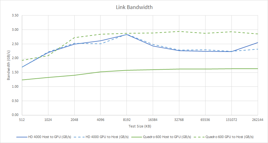
When using OpenCL to copy data between the CPU and GPU, both the HD 4000 and Nvidia’s Quadro 600 perform poorly. Nvidia’s card has a PCIe 2.0 x16 link to a FX-8150, via a 990FX chipset. It should be good for up to 8 GB/s of bandwidth, but I don’t get anything close. The HD 4000 should have a 32 byte/cycle interface to the ring bus, which is good for an order of magnitude more bandwidth. Unfortunately, this capability doesn’t shine until a couple of generations later.
Final Words
Despite a few high profile failures like i740 and Larrabee, Intel is no stranger to graphics. While ATI/AMD duked it out with Nvidia at the top end, Intel’s integrated GPUs quietly kept a huge chunk of the computing world running. These iGPUs didn’t have the power for serious gaming, but Intel was never far behind in terms of implementing the features required to run modern games. Gen 7 was part of an effort to keep Intel’s Gen line up to date. It introduces DirectX 11 support, and does a competent job at handling compute code. In doing this, it set a solid hardware foundation for Intel’s future graphics ambitions.
Features from Gen 7 continue to show up today. Subslices may have been renamed to Xe Cores, and EUs are now called Vector Engines. But Intel still has more internal subdivisions in their Xe Cores than AMD and Nvidia have in their equivalent blocks. Occupancy on Intel GPUs is still unaffected by register usage, with 128 registers per thread and 8 threads per EU (or Vector Engine). Ponte Vecchio introduces a “Large GRF” mode where a thread can have 256 registers while occupancy per EU drops to 4 threads, but the connection to Gen 7 is still there.
Thus, Intel’s latest foray into discrete graphics wasn’t out of the blue. Instead, it’s built on years of experience working on and improving the Gen architecture. Larger integrated GPUs like the ones in Ice Lake and Tiger Lake helped Intel develop more confidence, until they felt ready to go big. But building huge GPUs that deal with teraflops of compute and terabytes per second of bandwidth is quite outside Intel’s comfort zone. None of their integrated graphics experience would prepare them for such a task. Something as big as Ponte Vecchio will be very interesting to look at
If you like our articles and journalism, and you want to support us in our endeavors, then consider heading over to our Patreon or our PayPal if you want to toss a few bucks our way. If you would like to talk with the Chips and Cheese staff and the people behind the scenes, then consider joining our Discord.