AMD’s RX 7600: Small RDNA 3 Appears
Editor’s Note (6/14/2023): We have a new article that reevaluates the cache latency of Navi 31, so please refer to that article for some new latency data.
Late last year, AMD launched high end RDNA 3 with the Radeon RX 7900 XTX and Radeon RX 7900 XT. Now, they’ve rolling out smaller versions of RDNA 3 targeted towards more cost-conscious market segments. The Radeon RX 7600 replaces the Radeon RX 6600 XT in AMD’s lineup, providing slightly better performance. Reviewers generally agree that the RX 7600 is a disappointing product, because it doesn’t offer much better cost per frame than the outgoing RX 6600 XT, and will be limited by its 8 GB of VRAM. Thankfully (for us), Jiray has taken one for the team and bought a RX 7600 for testing.
AMD’s RX 7600 uses the Navi 33 chip, a monolithic design featuring 16 WGPs, 2 MB of L2 cache, and 32 MB of Infinity Cache. A 128-bit bus connects the die to 8 GB of GDDR6, providing 288 GB/s of theoretical VRAM bandwidth. That contrasts with Navi 31’s chiplet design, which puts 96 MB of Infinity Cache and 384-bits worth of memory controllers on separate dies. Navi 33 has less compute, cache, and memory controllers, which means a much smaller and low cost die. A complex chiplet setup with an interposer likely didn’t provide a cost benefit. On top of that, Navi 33 is fabricated on TSMC’s 6 nm node, not their cutting edge 5 nm process. TSMC’s 6 nm process is also used on Zen 4’s IO die and Navi 31’s memory controller dies. AMD’s Zen 4 CPUs and Navi 31’s graphics compute die use the more expensive 5 nm process, so Navi 33 definitely prioritizes low cost over maximum performance.
Architecture: RDNA 3 Lite
RDNA 3 is the third iteration of AMD’s RDNA line of GPU architectures, and features a set of improvements its workgroup processor (WGP), the architecture’s basic building block. We covered those in a previous article, where we talked about dual issue capability, the larger L0 vector cache, and vector register file capacity increase. These mostly apply to the RX 7600 too, but smaller RDNA 3 doesn’t get the larger register file.
Register files have to deliver exceptionally high bandwidth especially for vector execution. Having a larger register file potentially lets a GPU keep more work in flight, which is critical for hiding latency. However, AMD probably decided that the extra power and die area required to implement a larger register file wasn’t worthwhile for lower end products. Therefore, the RX 7600 has a 128 KB register file per SIMD, compared to the 192 KB register file found on the RX 7900 XTX. A WGP has four SIMDs, so the RX 7600 has 8 MB of vector registers across the entire GPU. For comparison, the 7900 XTX has 36.8 MB of vector registers.

As a result, the RX 7600’s WGPs may not be able to keep as many waves active, particularly if shaders ask for a lot of vector registers. They’re thus more likely to stall when dealing with long latency memory accesses because there’ll be fewer waves to pick from to find an un-stalled one. Rasterization will likely see minimal differences, as pixel shaders dominate rasterization workloads and tend to use very few vector registers.
For example, Valheim profiled on a RX 6900 XT shows excellent occupancy for pixel shaders. The longest duration shader only asked for 16 vector registers, which would allow maximum occupancy on both RDNA 3 variants.
VOPD Update
We have a long overdue update on RDNA 3’s dual issue capability. OpenCL testing in the previous article failed to reach full FP32 throughput because the compiler did not pack enough operations into VOPD dual issue instructions. When compiling my OpenCL test, there appears to be two issues – register allocation and VOPD evaluation distance. Register allocation refers to assigning ISA registers to hold values, and focuses on minimizing how often register contents are spilled to and reloaded from memory. However, this process is oblivious to VOPD packing restrictions. VOPD packing opportunities therefore depend on register allocation luck, and my code got a bad dice roll. Instruction level parallelism was available, but registers were allocated in a way that often made VOPD generation impossible.
We have to re-evalutate the result from Nemes’s Vulkan benchmark too. In the original article, I assumed the compiler was able to emit VOPD instructions in her test code. That assumption was incorrect. AMD’s driver ran the Vulkan code in wave64 mode, which naturally satisfies the register constraints for dual issue. Using environment variables to force wave64 mode allowed my OpenCL code to take advantage of dual issue. Changing the code so that each FMA operation took an immediate input (value directly encoded into the instruction) also let dual issue work even in wave32 mode.

The takeaway is that compilers really aren’t that smart. Compiler work is split into passes that perform specific tasks, like register allocation and final instruction generation. A human coding in assembly can see a bigger picture, and assign registers to create dual issue opportunities. Like higher end RDNA 3 cards, the RX 7600 will be subject to the compiler register allocation dice roll. And, it could benefit from “game-ready” drivers that replace game shaders with hand-optimized versions.
Frontend Clock Behavior
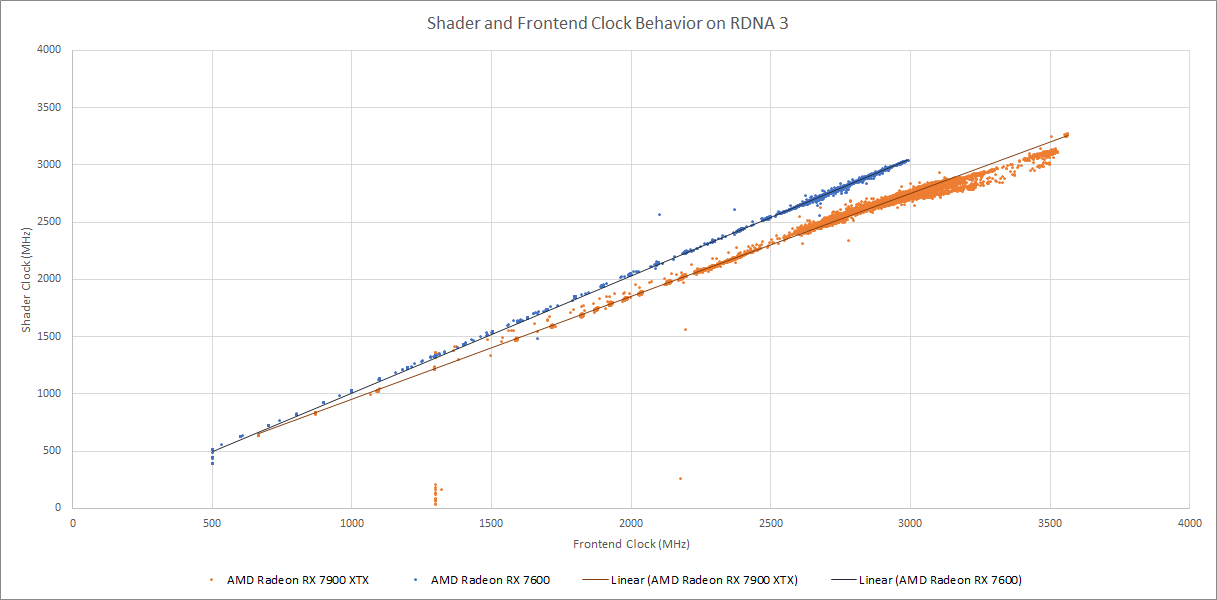
When designing RDNA 3, AMD found that workloads they analyzed were more limited by frontend work distribution and command processing than by shader engine throughput. To take advantage of this, they decoupled frontend clocks and shader clocks. RDNA 3 can therefore run frontend at higher clocks without the power cost of also clocking up the shader engine. In practice, high end RDNA 3 does exactly that. The 7900 XTX’s frontend generally clocks higher than the shader engine, and the gap increases at high clocks.

However, the RX 7600 takes a different strategy. Frontend clocks tend to be quite close to shader engine clocks. This behavior is quite consistent throughout the clock speed range. If we plot how much faster the frontend clocks compared to the shaders, with respect to shader clock, the pattern is even more obvious:
At the top end of the clock speed range, big RDNA 3 often clocks the frontend more than 10% faster than the shader engine. Even at more modern clock speeds, the frontend clocks 5-10% faster. In contrast, Navi 33 runs the frontend slower than the shader array. Perhaps the analysis AMD presented at the RDNA 3 launch presentation applies to large GPUs with gigantic shader arrays, but the situation is reversed with a GPU of the RX 7600’s size. Navi 33’s smaller shader array will take longer to finish work created by each command, so quickly processing commands and distributing work across the shader array is less critical.
Cache and Memory Latency
Since RDNA 2, AMD has used a complex, four-level cache hierarchy. Testing cache and memory latency is complicated, because AMD’s GPUs have separate datapaths and first level caches for scalar and vector accesses. From the scalar side, the new RX 7600 similar access latency to the fist level scalar cache. L1 and L2 latency is also similar from the scalar side, with the L1 cache getting a welcome capacity increase up to 256 KB. When we get to the Infinity Cache, the RX 7600 shows a very nice reduction in latency, with a similar latency reduction in VRAM.

From the vector side, we see RDNA 3’s L0 vector capacity increase to 32 KB. Elsewhere, results are largely similar to what we saw on the scalar side.
Nvidia’s Ada architecture takes a different approach with a large 32 MB L2, but sadly we’re not sure how that performs. Their prior Ampere architecture opts for a smaller L2, and relies on a beefier VRAM subsystem. Nvidia also uses a different first-level caching strategy, with L1 cache and shared memory allocated out of the same block of SRAM storage. The amount of L1 cache available will depend on how much shared memory the kernel requires. In this case, we don’t ask for any shared memory, so we get a large L1 cache allocation. AMD uses separate memories for their first level caches and local data share.
Small vs Big RDNA 3
Compared to its big brother, the RX 7600 sees similar latencies up to L2. However, the smaller GPU enjoys better Infinity Cache and VRAM latency. Smaller GPUs often enjoy better cache and memory latency, but the difference is especially large with RDNA 3. With RDNA 2, the RX 6900 XT had 151.57 ns of Infinity Cache latency compared to 130 ns on the RX 6600 XT, or a 16.5% latency penalty for the larger GPU. The 7900 XTX takes 58% longer to get data from its Infinity Cache than the 7600 XT. Navi 31’s chiplet configuration may be causing higher latency.
Vector accesses show a similar picture, though the gap is slightly smaller past L2. Latencies up to the L2 cache are quite close between the two GPUs, but a large gap opens up when we hit Infinity Cache. VRAM latencies are higher on the 7900 XTX too, but the absolute difference is similar for both VRAM and Infinity Cache. It’s possible that the RX 7600’s lower VRAM latency comes largely because getting to Infinity Cache takes longer on the 7900 XTX.

Navi 33’s lower latency Infinity Cache is interesting to look at next to its smaller register file. We mentioned before that a smaller vector register file can lead to lower occupancy, which in turn reduces latency hiding capability. Conveniently, Navi 33 has less latency to hide if it grabs data from the Infinity Cache. With good cache hitrates, a 50% register file capacity increase may bloat die area without providing a worthwhile performance boost. Of course, everything goes out the window if cache hitrates aren’t good.
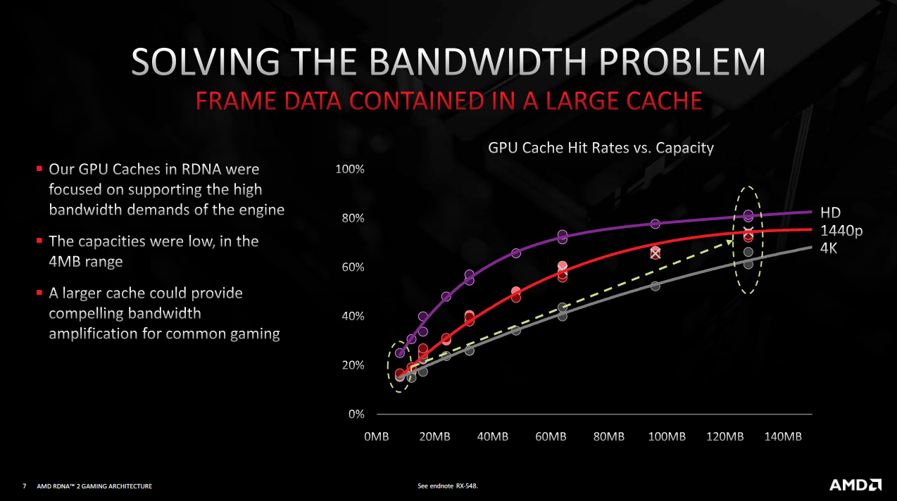
AMD’s data suggests that a 32 MB cache can provide decent hitrates at 1080P, which the RX 7600 targets. However, the same slide indicates that a 32 MB cache would struggle at higher resolutions. There, the RX 7600 could run into problems because it’d be eating VRAM latency while not enjoying the occupancy boost like its bigger brother does. Raytracing workloads could really suffer, because their vector register allocations tend to be high. With rasterization, where occupancy tends to be better, higher resolutions could still be problematic if low cache hitrates cause VRAM bandwidth bottlenecks.
Cache and Memory Bandwidth
But if accesses do hit cache, the RX 7600 enjoys excellent bandwidth at all shared cache levels. The L2 is the first cache level shared across the entire GPU, and has 2 MB of capacity on both the RX 7600 and RX 6600 XT. Bandwidth is very similar across the two generations, which is good because RDNA 2 had excellent L2 bandwidth. Technically, the RX 7600 XT won by 0.6% with 2.13 TB/s of measured L2 bandwidth, compared to 2.11 TB/s on the RX 6600 XT. But that’s well within margin of error, considering that clock speeds will probably vary by more than that during a gaming session.
Nvidia’s Ampere architecture takes a different approach, with a larger 4 MB L2 serving as the last level cache. Bandwidth isn’t as good as AMD’s, but the RTX 3060 Ti can still pull a nice 1.36 TB/s from L2. Thus, Nvidia’s 3060 Ti has almost as much L2 bandwidth as the venerable GTX 1080.
After L2, the RX 7600 and RX 6600 XT both feature a 32 MB Infinity Cache. Along with lower latency, the RX 7600 enjoys more bandwidth. Its Infinity Cache can provide 984 GB/s compared to 884 GB/s on the older card. Bandwidth scales almost identically on the two cards up to about 10 WGPs, but the RX 7600 has a clear advantage when all WGPs are loaded. Both cards have plenty of Infinity Cache bandwidth, because their L2 cache should absorb a lot of accesses.
Nvidia’s VRAM bandwidth is shown for reference here, since the RTX 3060 Ti doesn’t have a cache with similar capacity. Ampere strategy is different from RDNA 2 and RDNA 3’s, because Nvidia relies on a bigger memory setup. Moving to VRAM shows a large difference:
Nvidia’s RTX 3060 Ti enjoys a large VRAM bandwidth advantage. AMD did opt for faster GDDR6 on the RX 7600, giving it a small VRAM bandwidth edge over the RX 6600 XT. However, there’s no substitute for bus width, and the RTX 3060 Ti’s 256-bit bus puts it on a different level.
PCIe Link Bandwidth
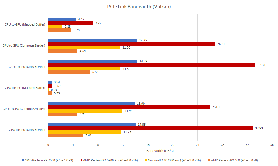
Bus width cuts go beyond the VRAM bus, and apply to the RX 7600’s PCIe link too. Unlike higher end discrete cards, the RX 7600 only has eight PCIe 4.0 lanes. That means it’ll have half as much bandwidth to the host system, but x8 PCIe setups are typical for x600 series cards as well as mobile GPUs. Fewer PCIe lanes save area, because IO interfaces don’t shrink very well with new process nodes. And, your gaming experience is probably ruined anyway if you have to keep going over the PCIe bus because you don’t have enough VRAM.
Thanks to PCIe 4.0, the RX 7600 has comparable host-to-GPU bandwidth as older GPUs using a x16 PCIe 3.0 interface. It also enjoys a large PCIe bandwidth advantage over older GPUs in the same market segment like the RX 460, which uses a 3.0 x8 interface.
Compute Throughput
The RX 7600 may be a small GPU, but RDNA 3’s dual issue capability gives it plenty of theoretical throughput. FP32 throughput can get quite close to the RX 6900 XT, RDNA 2’s top end GPU. That’s quite remarkable, because Navi 33 is implemented on a 204mm2 die, and didn’t benefit from a full node shrink. RDNA 3 is well suited to compute-bound workloads that can take advantage of dual issue, and that carries down to its smaller variants.
Less common operations don’t get a similar boost. Throughput for reciprocal, inverse square root, remainder, and divide operations look a lot like what we’d expect for a low end GPU.
Final Words
The RX 7600 provides a very interesting look at a low end, low cost RDNA 3 implementation. Like the prior generation’s RX 6600 XT, the RX 7600 implements 16 WGPs. It also has a small 32 MB Infinity Cache, a 128-bit memory bus, and eight PCIe lanes. Thus small configuration is necessary to reduce costs and power consumption compared to higher end cards.
But the RX 7600 goes even further to cut costs. It loses big RDNA 3’s bigger vector register file. It uses TSMC’s 6 nm process, which won’t provide the performance and power savings that the cutting edge 5 nm process would. In prior generations, AMD fabbed x60 and x600 series cards on the same cutting edge node as their higher end counterparts, and used the same architecture too. However, they clearly felt a sharp need to save costs with this generation, compromising the RX 7600 a bit more than would be expected for a midrange GPU.
On top of that, the RX 7600 doesn’t fully benefit from RDNA 3’s decoupled frontend and shader clocks. The two clock domains end up running at around the same frequency, possibly because the RX 7600’s smaller shader array can be well fed at lower shader clocks. In any case, the RX 7600 typically doesn’t reduce power by clocking down the shader array when the frontend’s the bottleneck.
But everything comes back to cost. These cost saving measures prevent the RX 7600 from being a compelling product at its launch price. Typically, a strong product launch will drive down prices for similarly placed products from the previous generation, because the new product delivers better value, performance, and power consumption. The RX 7600 largely fails to do that. It’s barely faster than the RX 6600 XT while offering similar value. Power efficiency didn’t improve either, which isn’t a surprise because TSMC’s 6 nm node doesn’t offer a performance or efficiency gain over 7 nm.
In AMD’s favor, the RX 7600 does give you RDNA 3’s architecture improvements and features. AV1 support and better raytracing performance count for something. But these value adds should be icing on the cake because they only apply to specific situations. A new product needs to provide value, performance and power improvements across the board. It needs to be so good that it pushes down prices for previous generation products in the same segment. The RX 7600 doesn’t do that. Considering all of the cost cutting measures, the RX 7600 really should be cheaper.
Nvidia also launched the RTX 4060 Ti recently, with even worse performance per dollar. The midrange GPU market today is a dumpster fire. I hope AMD and Nvidia will cut prices to make their current generation products more compelling, and make bigger leaps with their future GPUs.
If you like our articles and journalism, and you want to support us in our endeavors, then consider heading over to our Patreon or our PayPal if you want to toss a few bucks our way. If you would like to talk with the Chips and Cheese staff and the people behind the scenes, then consider joining our Discord.


