


AMD’s HD 6950 vs RX 6900 XT: What Does Adding 50 Do?

Note the publish day of this article. There will be a proper one on Terascale 3 later on, don’t worry. But for now, happy April Fools Day!
Prestige is everything for computer hardware manufacturers. A few percentage points may not make or break someone’s gaming experience, or make some new workload accessible to the masses; but it does boost a manufacturer’s reputation. A tangential question, then, is what would happen if we increased the model number by a few percentage points. 6950 is 0.7% higher than 6900, after all. So, what does such an increase to the model number get you?
Fortunately, we can figure this out in all the detail we’re used to. I have an AMD Radeon HD 6950 to compare to the Radeon RX 6900 XT. Ideally I would compare the 6950 XT and 6900 XT, but that would cost money.
Comparing Architectural Building Blocks
The Radeon HD 6950 and Radeon RX 6900XT use very different architectures, even though both products belong to the 6000 series and share a brand name. AMD’s Radeon HD 6950 uses the Terascale 3 architecture. Terascale 3’s building blocks are called SIMD Engines, and the HD 6950 has 22 of them enabled out of 24 on the die. Like GCN, Terascale 3 runs in wave64 mode. That means each instruction works across a 64-wide vector. Each element is 32 bits wide, making it a bit like AVX-2048.
Because the SIMD Engine has a 16-lane execution unit, the 64-wide wave is executed over four cycles. A single thread can’t execute instructions back to back because of register port conflicts, so instructions effectively have eight cycle minimum latency, and a SIMD engine needs at least two waves in flight to keep the execution unit busy. Each execution lane is VLIW4, meaning it’s four components wide; so the SIMD can execute 64 FP32 operations per cycle. With VLIW packing in mind, a SIMD would need 64 * 2 * 4 = 512 operations in flight in order to reach its maximum compute throughput.
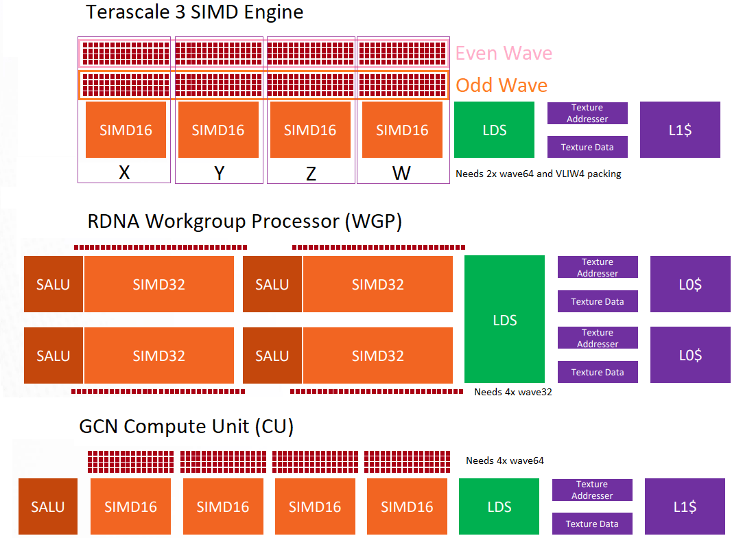
In contrast, RDNA 2 focuses on making the execution units easy to feed. It uses much larger building blocks as well, called Workgroup Processors, or WGPs. Each WGP consists of four 32-wide SIMDs, which can execute either wave32 or wave64 instructions. These SIMDs are comparable to Terascale’s SIMD engines, in that both have their scheduler feeding an execution unit. However, RDNA 2 SIMDs are far easier to feed. They can complete a 32-wide wave every cycle, and execute instructions from the same thread back to back. They don’t need VLIW packing either. In fact, a WGP with 128 FP32 lanes only needs 128 operations in flight to fully utilize those execution units.
Instruction Throughput
Terascale 3 and RDNA 2 have different priorities when it comes to execution unit design. For a fairer comparison, the 6900 XT is forced into CU mode for instruction rate testing. That means the LDS is partitioned into two 64 KB sections. If we run a single workgroup, it has to stay on one half of a WGP, with 64 lanes. Comparisons are easier if we can compare 64 lanes to 64 lanes, right? I’ve also locked the 6900 XT to the same 800 MHz clock speed so I can divide by 0.8 for per-cycle throughput across both GPUs, saving a few keypresses in Excel.
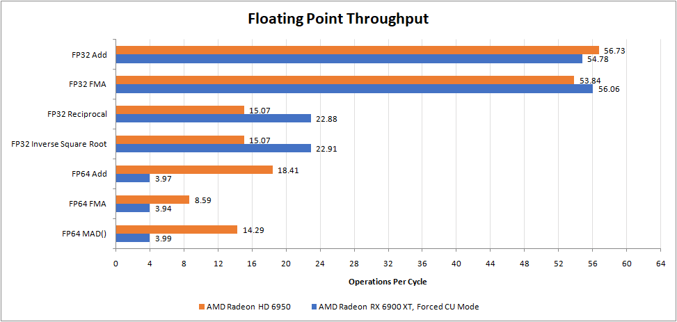
The HD 6950 has impressive FP64 performance, though it does take a bit of coaxing to get maximum performance out of the design. AMD’s old driver is prone to translating a * b + c into separate FP64 multiplies and adds. It won’t emit a FMA_64 instruction unless you use the OpenCL MAD() function, which prefers speed over accuracy. Therefore, you have to be MAD to get the most out of Terascale 3’s FP64 performance. But even if you dislike being MAD, Terascale 3 is still a very competent FP64 performer compared to RDNA 2.
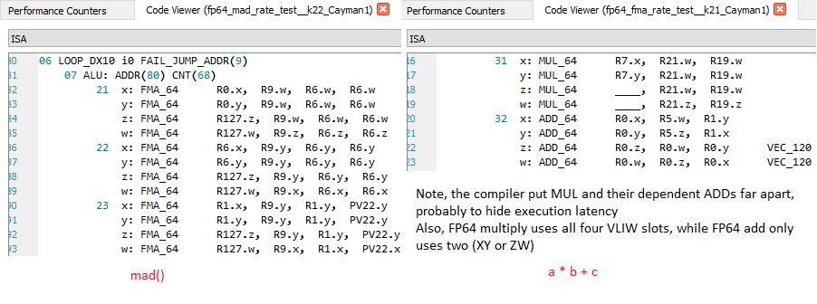
Under the hood, Terascale 3’s register file is organized into four banks, named X, Y, Z, and W. FP64 is dealt with by using the corresponding registers in a pair of banks to store a 64-bit value, and using a pair of VLIW lanes (XY or ZW) to perform the calculation. Each VLIW lane can only write a result to its corresponding register bank, and the same restriction applies for FP64.
For comparison, the 6900 XT is a terrible FP64 performer. The HD 6950 came out at a time when people were wondering if GPU compute would be widely used, with some fantasizing about GPUs acting like a second FPU. Good FP64 throughput would be useful for offloading a wider variety of workloads, because FP64 is used a lot with CPUs. In contrast, RDNA 2 came out when GPU compute was clearly a secondary role for consumers.
RDNA 2 has an advantage with special functions like reciprocal and inverse square root, though funny enough the throughput for these functions did not change between CU mode and WGP mode. Maybe there’s one 32-wide unit shared across the entire WGP, who knows.
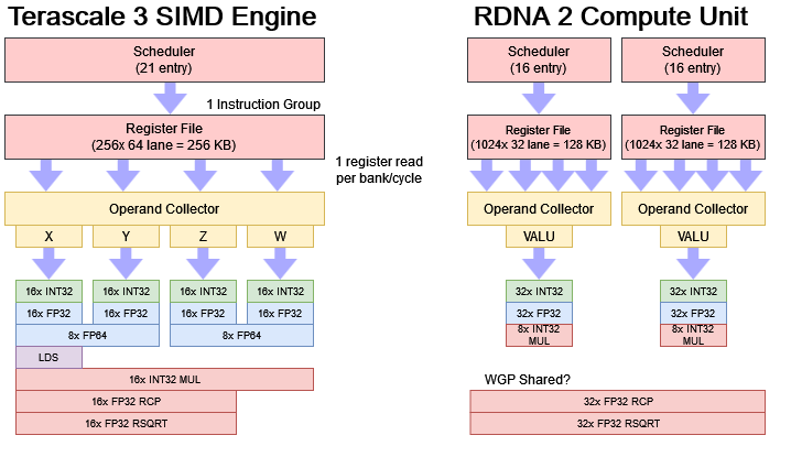
The same does not apply to 32-bit integer multiplication, which is also treated as a special function of sorts for both architectures. It has a lot less throughput. Like other special functions on Terascale 3, integer multiplication is executed by issuing one instruction across several of the VLIW lanes. Older Terascale variants had a separate T lane for handling special functions, but that lane was often hard to feed due to register bandwidth constraints and instruction level parallelism limitations.
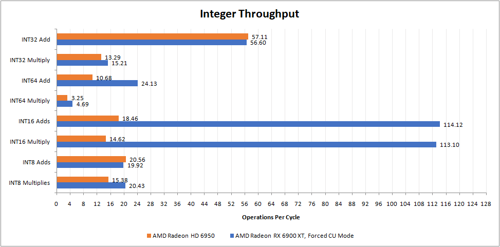
Both architectures can execute the more common 32-bit integer adds at full rate. RDNA 2 has a large advantage for 16-bit integer operations, because it can pack two of them into one 32-bit register, and can configure the integer ALU to execute that at double rate. In contrast, Terascale 3 has no 16-bit integer ALUs. It simply reuses the 32-bit ALUs for lower precision operations, and then masks the results (or uses bitfield insert) to get a 16-bit value.
For 64-bit integer operations, both architectures use add-with-carry instructions because they don’t have 64-bit vector integer ALUs. In theory, both should execute them at half rate. But remember that little detail about how each Terascale lane can only write to its corresponding register bank? AMD’s compiler ends up wasting ALU slots to move register values around, lowering throughput.
Caches
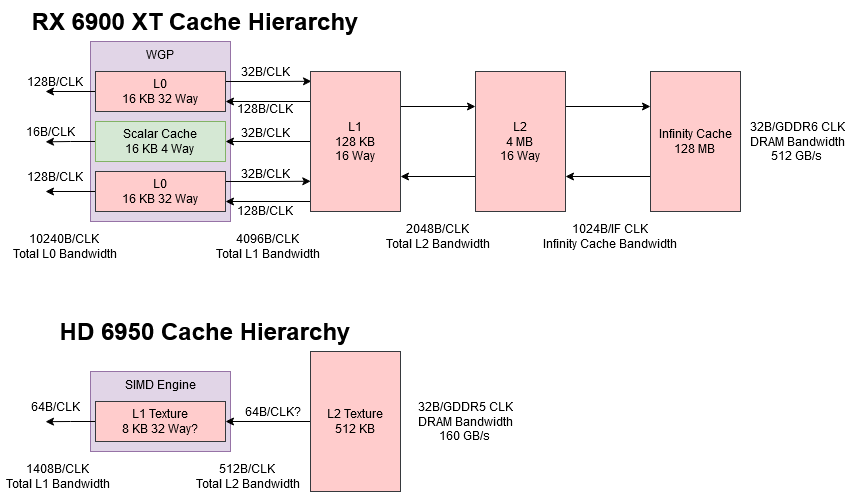
Having execution units is fun, but feeding them is not. Again RDNA 2 emphasizes feeding the execution units. It has a complex cache hierarchy with more cache levels than your typical CPU. Each pair of SIMDs has a 16 KB L0 cache, which acts as a first level cache for all kinds of memory accesses. Each shader engine has a 128 KB L1 cache, which primarily serves to catch L0 misses and simplify routing to L2. Then, a 4 MB L2 serves as the first, GPU-wide read-write cache with multi-megabyte capacity. Finally, a 128 MB Infinity Cache helps reduce memory bandwidth demands. RDNA 2’s caches are highly optimized for both graphics and compute. Non-texture accesses can bypass the texture units, enabling lower latency.
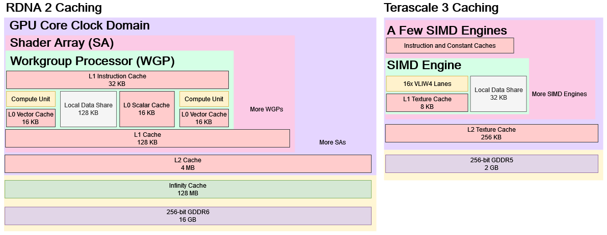
To further improve compute performance, RDNA 2 has separate vector and scalar caches. On the vector side, the WGP’s four SIMDs are split into two pairs, each with its own vector cache. That arrangement allows higher bandwidth, compared to a hypothetical setup where all four SIMDs are hammering a single cache. 128B cache lines further help vector cache bandwidth, because only a single tag check is needed to get a full 32-wide wave of data. On the scalar side, there’s a single 16 KB cache optimized for low latency. It uses 64B cache lines and is shared across the entire WGP, helping to make more efficient use of cache capacity for stuff like shared constants.
Terascale 3 is the opposite. It has a simple two-level cache hierarchy, with small caches all around. Each SIMD engine has a 8 KB L1 cache, and the whole GPU shares a 256 KB L2. There’s no separate scalar memory path for values that stay constant across an a wave. Unlike RDNA’s general purpose caches, Terascale’s caches trace their lineage to texture caches in pre-unified-shader days. They’re not optimized for low latency. Memory loads for compute kernels basically execute as vertex fetches, while RDNA 2 can use specialized s_load_dword or global_load_dword instructions that bypass the TMUs.
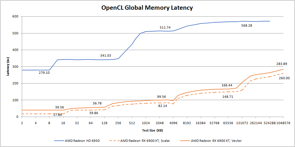
We can’t completely blame the caches either. Terascale 3 organizes different types of instructions into clauses. It has to switch to a texture clause to fetch data from caches or VRAM, then to an ALU clause to actually use the data. A clause switch carries significant latency penalties. Terascale instructions themselves suffer from high latency because they execute over four cycles, and then have to wait four more cycles before the thread can execute again. That means address generation takes longer on Terascale. RDNA 2 is far better in this regard because it doesn’t have a clause switch latency and can execute instructions with lower latency. To make things worse for Terascale 3, RDNA 2 clocks more than twice as high even though it has a lower model number.
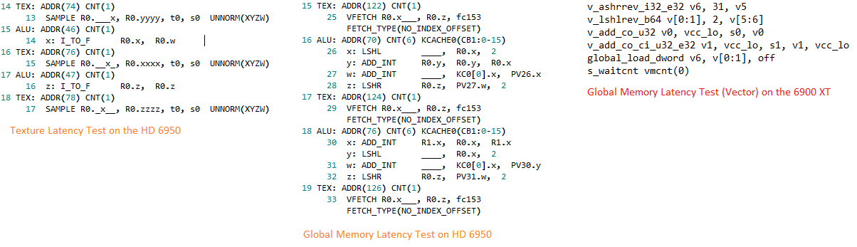
But a higher model number does help in one case. Relatively speaking, Terascale 3 is better if we use texture accesses. That’s because we’re using the TMUs to help with address generation, instead of working against them. Still, the HD 6950’s latency is brutal in an absolute sense.
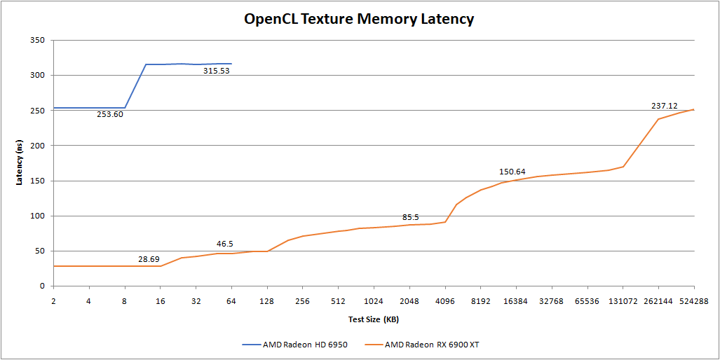
RDNA 2 takes a surprisingly light penalty from hitting the TMUs.The buffer_load_dword instructions take longer than the scalar s_load_dword ones, but they actually do better than vector accesses (global_load_dword).
Local Memory (LDS)
When GPU programs need consistent, low latency accesses, they can bring data into local memory. Local memory is only shared between small groups of threads, and acts as a small, high speed scratchpad. On AMD GPUs, local memory maps to a structure called the Local Data Share (LDS). Each Terascale 3 SIMD Engine has a 32 KB LDS, while each RDNA 2 WGP has a 128 KB LDS.
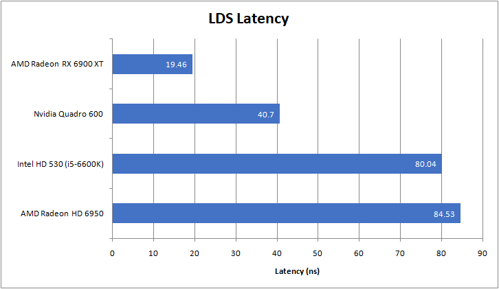
Unfortunately, a higher model number does not help and Terascale’s LDS has more than four times as much latency as RDNA 2’s. However, the HD 6950 does end up somewhere near Intel’s HD 530. So maybe, a higher model number has benefits, because it brings you closer to where a bigger company was.
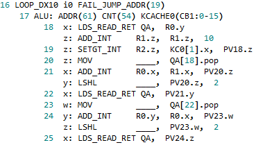
Also, what about LDS bandwidth? Terascale 3’s LDS can deliver 128 bytes per cycle to its SIMD Engine. RDNA 2’s LDS can send 128 bytes per cycle to each pair of SIMDs. Unfortunately testing bandwidth is hard because of address generation overhead and needing to do something with the results so the compiler doesn’t optimize it out. But here’s an early attempt:
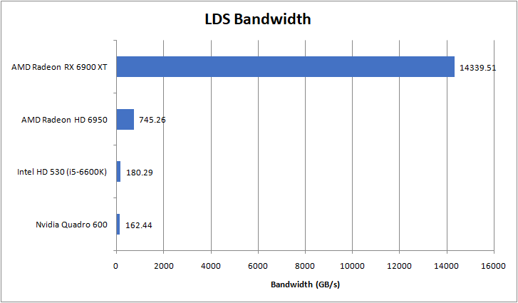
Nope. We’re really starting to see that adding 50 to the model number doesn’t help. 6950 is over 13 times higher than 530 though, so maybe there’s still an advantage. More specifically the HD 530’s three subslices each have a 64 byte per cycle data port to both the LDS and L3. Contrast that with Terascale, which has a 128 byte per cycle path to the LDS within each SIMD. I guess if your model number is too low, you make nonsensical architectural choices.
Cache Bandwidth
From a single building block’s perspective, RDNA 2 has a massive advantage. The HD 6950 may have a higher model number, but the 6900 XT benefits from higher – much higher – clock speeds, a more modern cache hierarchy, and bigger building blocks. A WGP simply has more lanes than a SIMD Engine. It’s nice to see the cache hierarchy again from a bandwidth perspective. But just as with latency, the HD 6950 gets destroyed.
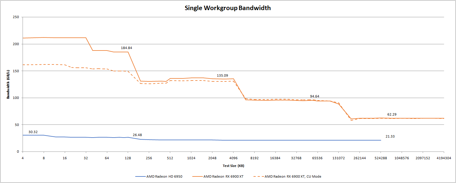
A higher model number may be great for marketing, but clearly it means smaller building blocks and a weaker cache hierarchy. But even if we set the 6900 XT to CU mode, 64 lanes fare far better with the same level of parallelism.
Let’s look at shared parts of the memory hierarchy too, and how they handle bandwidth demands as more SIMD Engines or WGPs get loaded up. Most parts of graphics workloads are highly parallel, so shared caches have the unenviable job of servicing a lot of high bandwidth consumers.
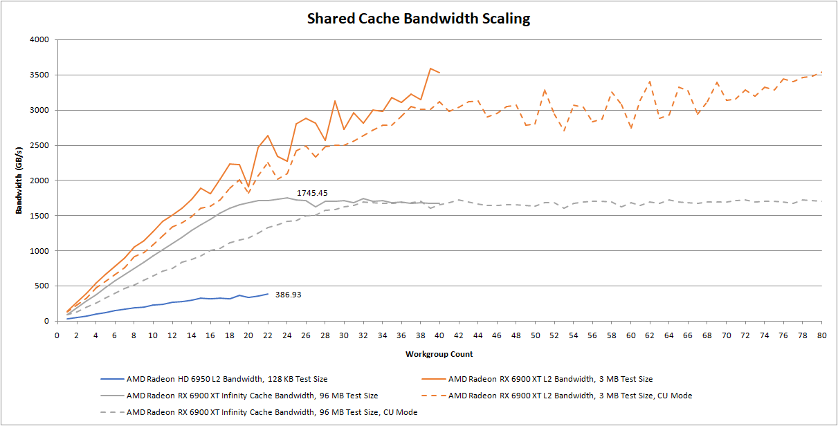
Again, Terascale 3 gets utterly crushed. The L2 tests are the most comparable ones here, because it’s the first cache level shared across the entire GPU. The 6900 XT can deliver around ten times as much L2 bandwidth despite having a lower model number. RDNA 2’s performance advantage here is actually understated because it has a write-back L2 cache. Terascale 3’s L2 is a texture cache, meaning that it can’t handle writes from the shader array. Writes do go through some write coalescing caches on the way to VRAM, but as their name suggests, those caches are not large enough to insulate VRAM from write bandwidth demands.
RDNA 2 has an additional level of cache beyond L2. With 128 MB of capacity, the Infinity Cache primarily serves to reduce VRAM bandwidth demands. In other words, it trades die area to enable a cheaper VRAM setup. Even though Infinity Cache doesn’t serve the same role as the L2, it’s also a shared cache tied to a memory controller partition. It also stomps the HD 6950’s L2 by a massive margin. CU mode takes a little longer to ramp up, but eventually gets to the same staggering bandwidth.
Out in VRAM, the HD 6950 does relatively better. It still loses, but only by a 3x margin. The higher mode number does count for something here because Terascale 3 can deliver more bytes per FLOP, potentially meaning it’s less bandwidth bound for larger working sets. That is, if you don’t run out of VRAM in the first place.
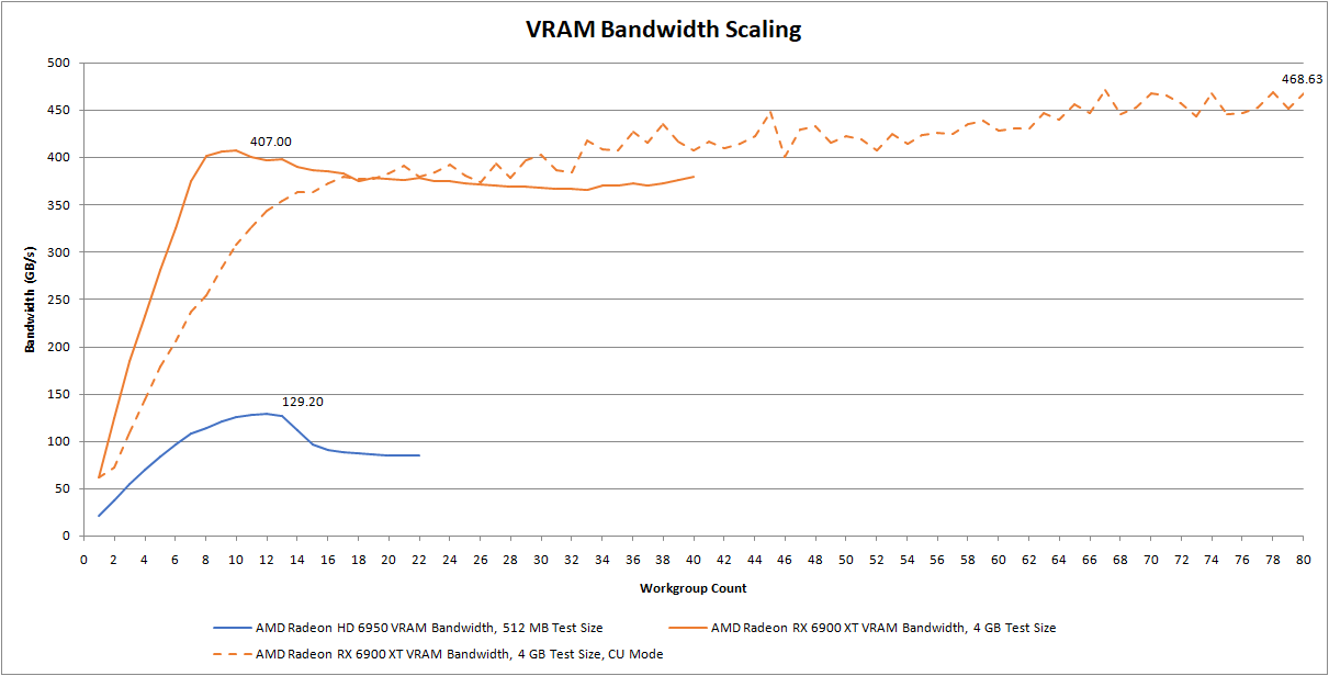
Still, the 6900 XT has a massive bandwidth advantage in absolute terms. GDDR6 can provide far more bandwidth than GDDR5.
What About Bigger Numbers
So far, we’ve seen that adding 50 to the model number has not produced any real advantages. The HD 6950 may be relatively efficient in terms of using very little control logic to enable a lot of compute throughput. It might have more VRAM bandwidth relative to its FP32 throughput. But the 6900 XT is better in an absolute sense, across all of those areas. Some of this can be attributed to the process node too. On that note, TSMC’s 40 nm process has a bigger number than their 7 nm process. But again, bigger numbers don’t help.
Yet, AMD’s most recent card has increased model numbers even further. The RX 7900 XTX’s model number is 1000 higher than the RX 6900 XT’s. Such a massive increase in the model number has created more downsides. Even though the HD 6950 has a higher model number, it wasn’t high enough to cause issues with clock speeds.
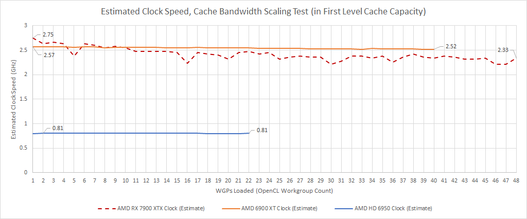
But incrementing the model number by such a massive amount impacted clocks too. Normally we don’t look at first level cache bandwidth scaling, because it’s boring. Each SM or CU or WGP or SIMD Engine has its own first level cache, so you get a straight line and straight is not cool.
But that changes with RDNA 3. If all of the WGPs are loaded, clocks drop by more than 15%. Clock drops are not a good thing. If RDNA 3 could hold 3 GHz clocks across all workloads, it would compete with the RTX 4090. In the same way, the Ryzen 9 7950X would dominate everything if it could hold 5.7 GHz regardless of how many cores are loaded. This clocking behavior is definitely because of the higher model number.
If AMD went with a lower model number, RDNA 3 would be able to maintain high clock speeds under heavy load, just as the 6950 and 6900 did. Unfortunately, AMD used 7950 for their top end RDNA 3 card. If they didn’t, a 15% clock increase might let them compete directly with the RTX 4090.
Conclusion
AMD should not continue to increase model numbers. Doing so can decrease performance across a variety of metrics, as data from the HD 6950 and RX 6900 XT shows. Instead, they should hold the model number in place or even decrease it to ensure future generations perform optimally.
If AMD keeps the model number constant, what could they do to properly differentiate a new card? Well, the answer appears to be suffixes.
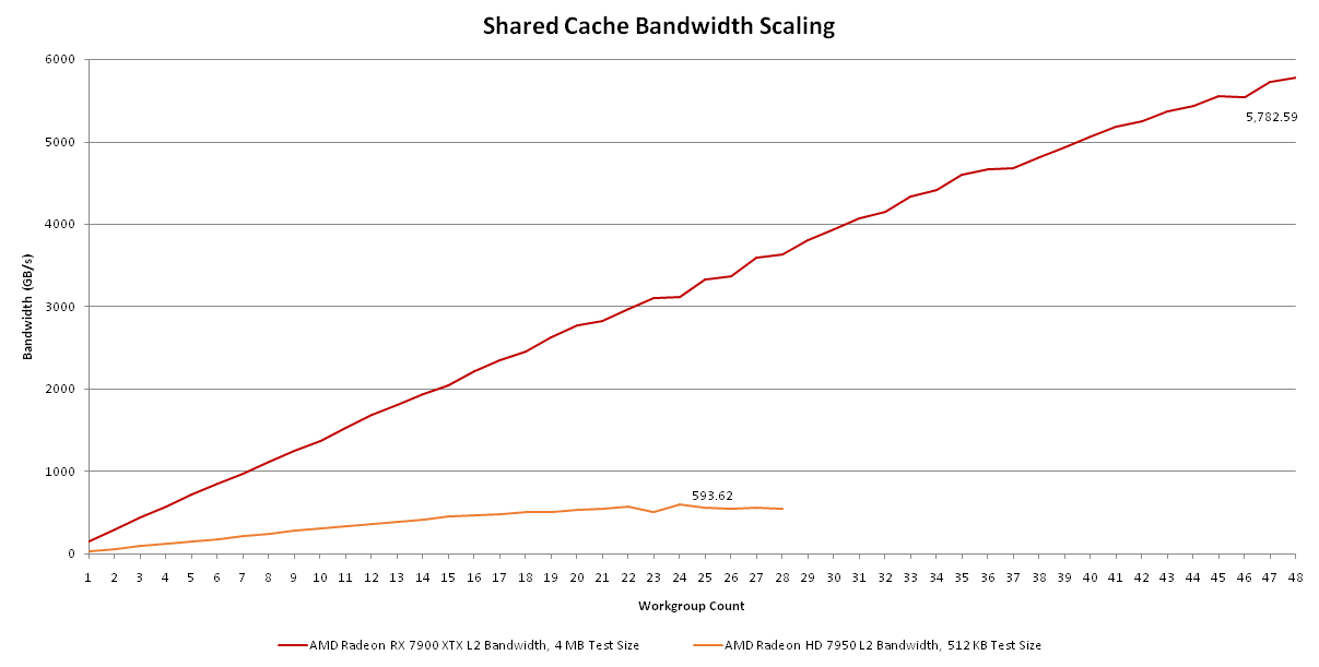
Adding a ‘XTX’ suffix has given RDNA 3 a gigantic cache bandwidth lead over the HD 7950. The same advantage applies elsewhere. For their next generation, AMD should release a Radeon RX 7900 Ti XTX SE Pro VIVO Founders Edition in order to get the suffix advantages, without the model number increase disadvantages.
However, AMD should be cautious about adding too many suffixes. Going from the 6950 to the 6900 XT increased the number of power connectors from two to three. A hypothetical Radeon RX 7900 Ti XTX SE Pro VIVO Founders Edition may have eight power connectors. Consumers running budget supplies may not be able to use the card, unless they make ample use of six-pin to eight-pin adapters, and eight-pin to dual eight-pin adapters after that. On an unrelated note, always make sure you check the link target before you click and buy.
If you like our articles and journalism, and you want to support us in our endeavors, then consider heading over to our Patreon or our PayPal if you want to toss a few bucks our way. If you would like to talk with the Chips and Cheese staff and the people behind the scenes, then consider joining our Discord.
Great article, loved the humor! A quick question regarding your block diagrams for Terrascale's simd engines. The layout of the ALUs from what AMD had always provided suggests the simd blocks are configured as XYZW *16, while yours look like X*16, Y*16, Z*16, W*16.