
Raytracing on AMD’s RDNA 2/3, and Nvidia’s Turing and Pascal

Note: Jake has commented that Nvidia’s tools may not show the true BVH structure. That’s a distinct possibility, as the structure implied by Nsight is indeed ridiculously wide. The rest of the article will be left unedited (for now) due to time constraints, but consider the original conclusion that Nvidia’s using a wider BVH unsubstantiated.
Raytracing aims to accurately model light by following the paths of light rays and seeing what they hit. However, raytracing is quite expensive compared to say, calculating light values by taking a pixel’s distance to light sources and doing an inverse square root. You need to send off a lot of rays to get enough rays to hit each pixel. On top of that, a ray could potentially hit any object in the scene. Obviously, you don’t want to do intersection tests against every piece of geometry. That’s where a bounding volume hierarchy (BVH) comes to implement a divide-and-conquer approach to seeing what a ray hits.
A BVH is a tree, or a structure where each node connects to several child nodes. Your GPU starts at the node at the top of the tree, and checks whether the ray in question intersects any child nodes. If it does, it follows those child links and repeats the process until it gets to the bottom of the tree. Each child node represents a rectangular region, which is why these upper level nodes are often called box nodes. The bottom nodes, also known as leaf nodes, contain geometry primitives that are checked to determine if the ray actually hit something. These geometry primitives are triangles, so the leaf nodes are also known as triangle nodes.
The concept is quite simple, but there’s a lot of different ways you can build a BVH. If you put more boxes into a box node, you can subdivide the scene more. But that means more computation (intersection tests) at each level. You can make more levels to cut down on computational costs, but then you’d make more jumps from one node to another. Here, we’re going to use developer tools from both AMD and Nvidia to take a peek at how each manufacturer has chosen to build their BVH-es.
AMD RDNA 2 and RDNA 3
AMD implements raytracing acceleration by adding intersection test instructions to the texture units. Instead of dealing with textures though, these instructions take a box or triangle node in a predefined format. Box nodes can represent four boxes, and triangle nodes can represent four triangles. The instruction computes intersection test results for everything in that node, and hands the results back to the shader. Then, the shader is responsible for traversing the BVH and handing the next node to the texture units. RDNA 3 additionally has specialized LDS instructions to make managing the traversal stack faster.
Cyberpunk 2077
Cyberpunk 2077 can make extensive use of raytracing, and is one of the best showcases of what the technology can enable. Turning on raytracing often produces an immediately noticeable difference, as reflections that the game doesn’t handle with rasterization become visible. To do raytracing, Cyberpunk 2077 uses the DirectX Raytracing (DXR) API. It defines BVH-es in two structures – a top level acceleration structures (TLAS), and a bottom level acceleration structure (BLAS). Traversing the TLAS gets you to a BLAS, which eventually gets you to the relevant geometry.
With a capture from inside “The Mox”, we get a TLAS that covers a massive portion of the gameplay setting. Most of Night City seems to be included, as well as the surrounding areas. The TLAS has 70,720 nodes, of which 22,404 are box nodes and 48,316 are “instance nodes” that link to BLAS instances. Traversing the TLAS leads you to 8,315 BLAS instances, which collectively represent 11,975,029 triangles. The TLAS occupies 11 MB of storage, while everything together (including the BLAS-es) occupies 795 MB.
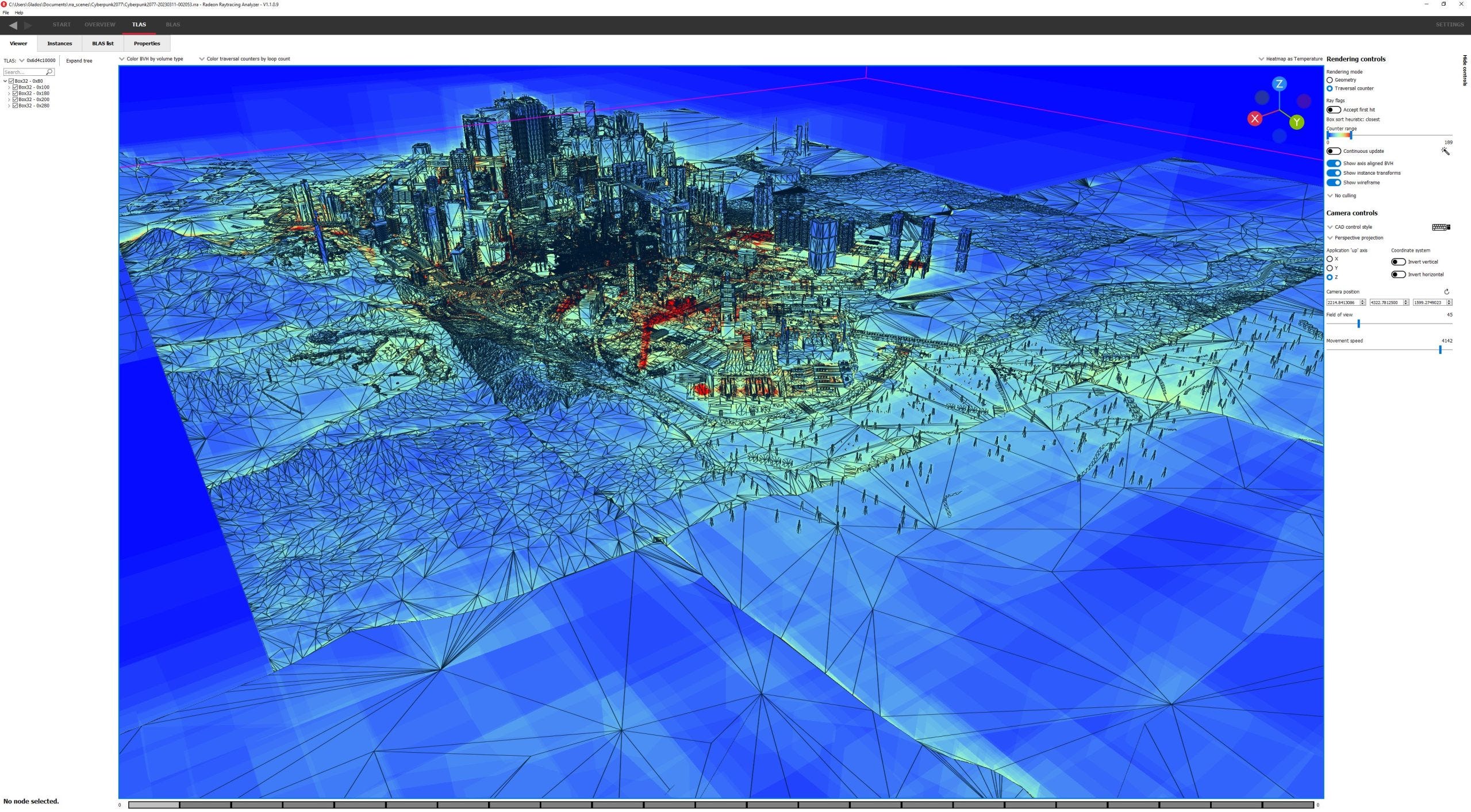
The first level of four bounding boxes divide the city into two parts, and the large unoccupied area at the bottom of the screen into two parts as well. Those areas don’t have a lot of geometry to do further subdivision on, so the TLAS only goes a couple levels deeper before you get BLAS pointers.
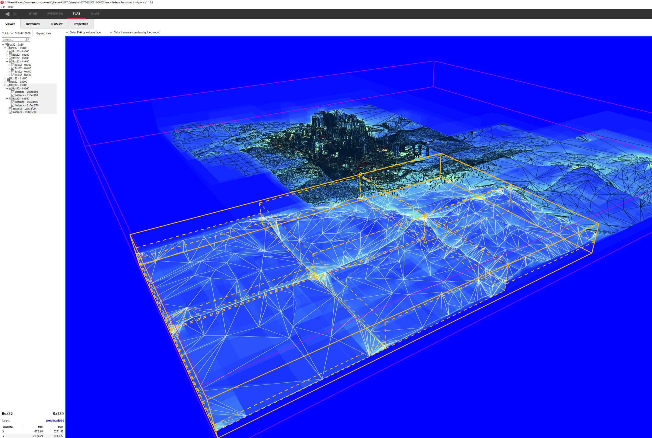
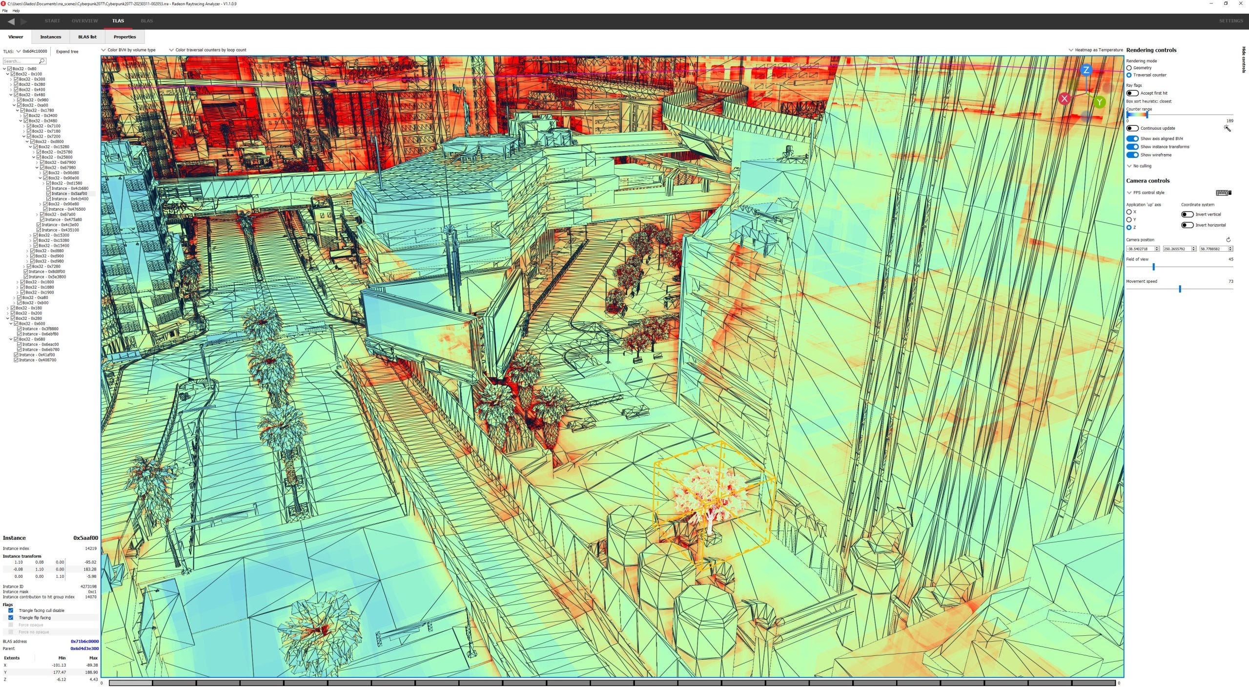
Of course, the city is the fun part. Zooming into the depths of Night City, we see a tree represented by a BLAS. To be clear, I’m talking about a tree in the game, not a data structure. Cache and memory latency is going to be a concern here, because getting to the BLAS requires 12 pointer chasing jumps between nodes.
Within the BLAS, taking another six jumps gets you to a triangle node, or leaf node, with four triangles. Each triangle probably represents a set of leaves on the actual tree. From the top, getting to the actual geometry takes 19 hops, including jumping from the TLAS to the BLAS.
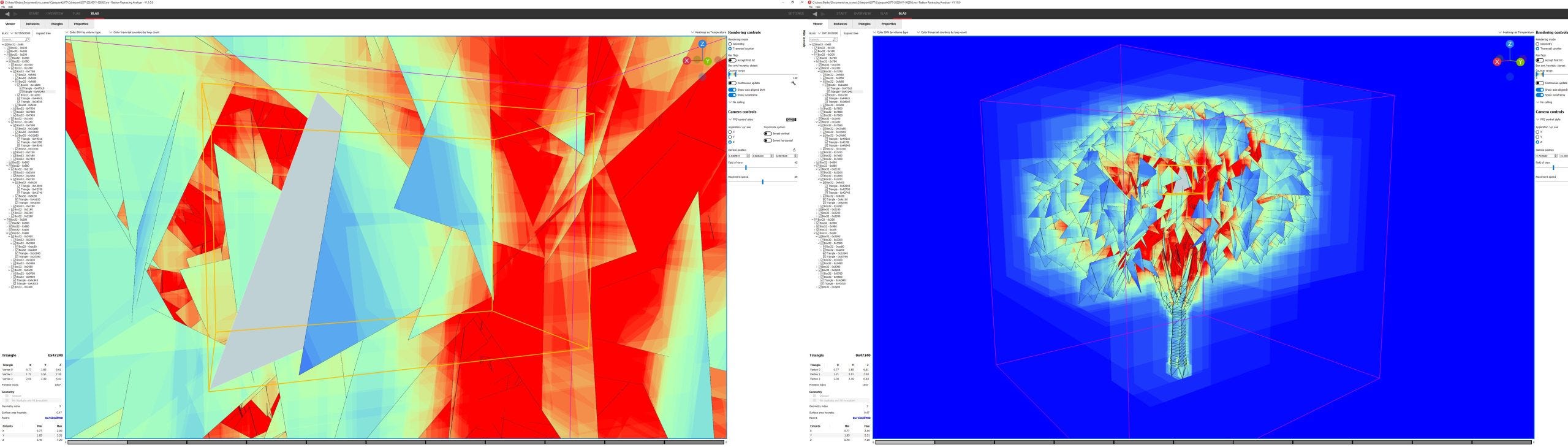
AMD thus uses a rather deep BVH with a lot of subdividing. That means less demand on intersection test throughput. But cache and memory latency will have a large impact, because each jump between nodes is dependent on the intersection test results from the previous node. GPUs have high cache and memory latency compared to CPUs, so RDNA 2 will need to keep a lot of rays in flight to hide that latency.
We previously looked at how RDNA 2 handled raytracing at the hardware level, and noted that the L2 cache played a very significant role. Looking at the raytracing structure sizes, the hitrates we saw make a lot of sense. The TLAS alone is 11 MB, so unless a lot of rays happen to go in the same direction, caches with capacities in the kilobyte range will probably have difficulty coping.

Our testing also shows that the RX 6900 XT’s L2 cache has a load-to-use latency of just above 80 ns. While that’s good for a multi-megabyte GPU cache, it’s close to memory latency for CPUs. In the end, the 6900 XT was averaging 28.7 billion box tests and 3.21 billion triangle tests per second during that call, despite being underclocked to 1800 MHz. AMD says each CU can perform four box tests or one triangle test per cycle, so RT core utilization could be anywhere from 7.2% to 29% depending on whether the counters increment for every intersection test, or every node.

Ideally, AMD would keep more rays in flight to hide latency and increase execution unit utilization, but vector register file capacity limits occupancy to 10 waves per SIMD out of the 16 maximum. That’s one motivation behind RDNA 3 increased vector register file capacity. Checking Cyberpunk 2077 through RDNA 3’s lenses, we see occupancy increase to 12/16.

Furthermore, RDNA 3 enjoys a noticeable increase in L0 and L1 hitrates. Those caches have doubled in size compared to RDNA 2, while also offering improved latency. RDNA 3 ends up averaging 45.2 billion box tests and 5.22 billion triangle tests per second in that shader. That’s quite an impressive performance uplift, though it’s hard to quantify the difference in RT core utilization because the 7900 XTX was not locked to known clocks.
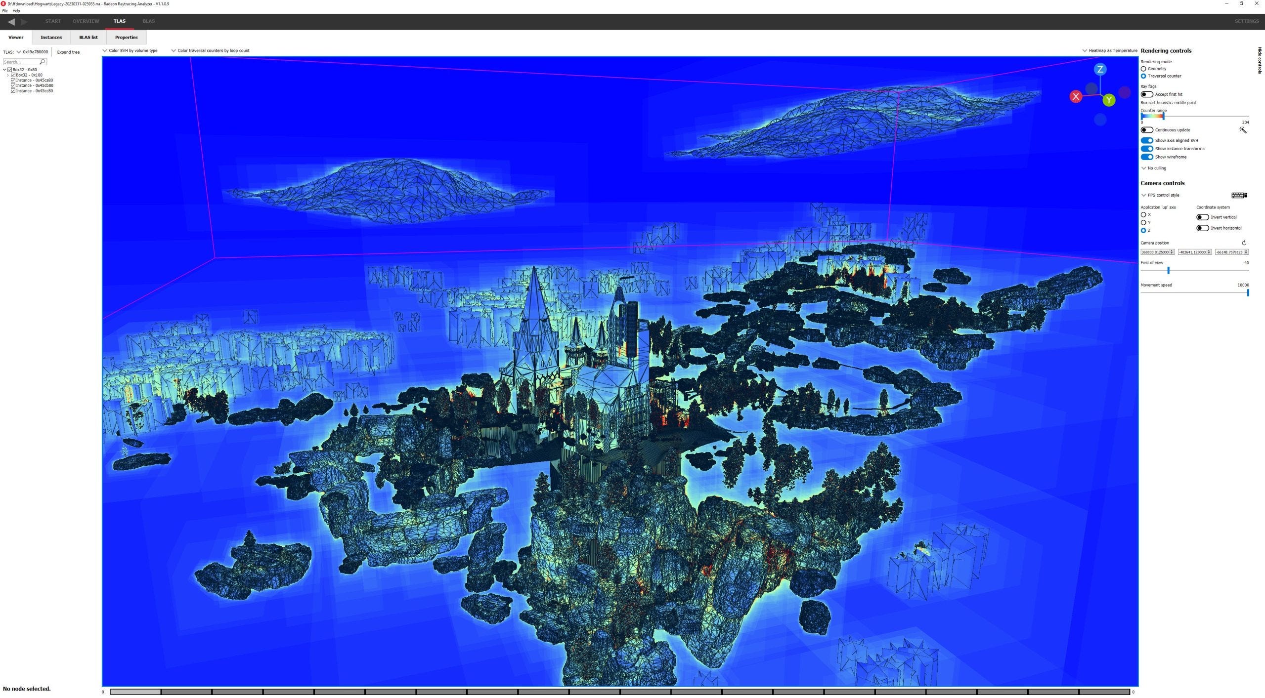
Hogwarts Legacy
Hogwarts Legacy is a recent game release that also makes use of raytracing. Titanic has done profiling on this game using his 7900 XTX, since I don’t own the game. Both Hogwarts Legacy and Cyberpunk 2077 feature similar TLAS sizes, but Hogwarts has a much smaller memory footprint when you consider the BLAS-es.

Just as with Cyberpunk 2077, the TLAS covers a massive amount of area. In Hogwarts Legacy, it appears to include Hogwarts Castle as well as the surrounding grounds, and some far-off mountains. The mountains don’t have a lot of complex geometry and are covered by a single box (and BLAS). Three of the four boxes at the top level cover the mountains, and one covers most of the gameplay area.
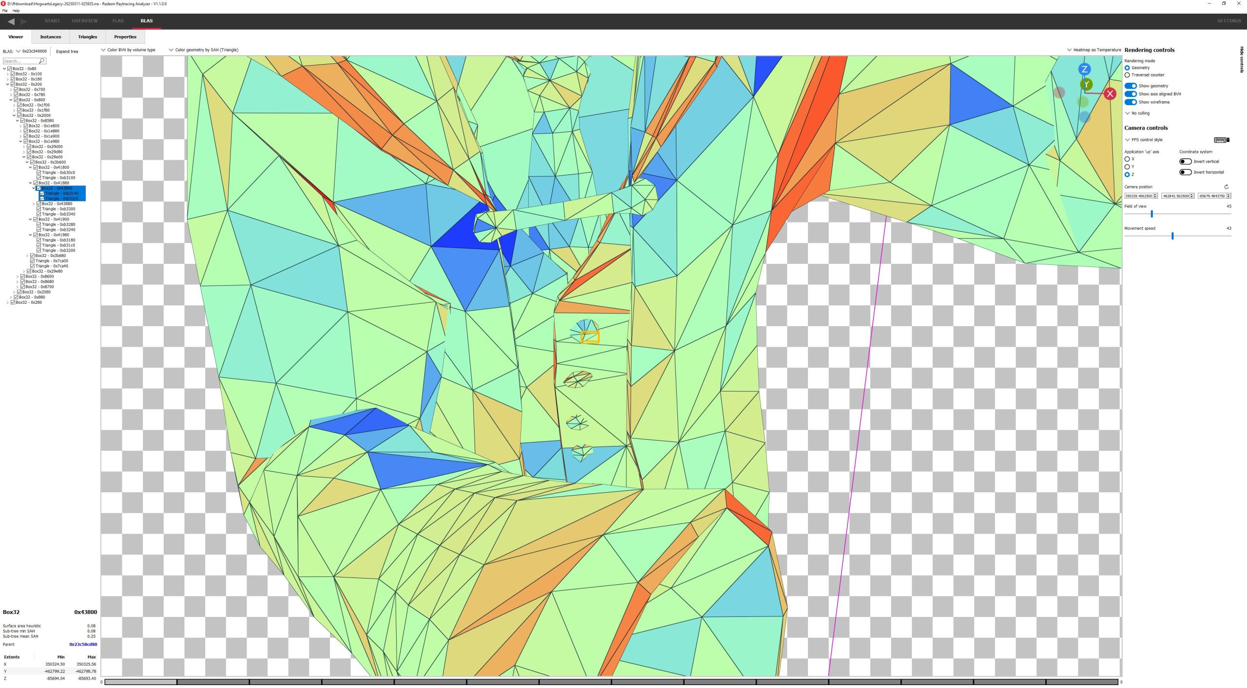
Titanic took the capture from the courtyard. Zooming into that area reveals a massive amount of geometric detail, including animate objects like humans and a cat.
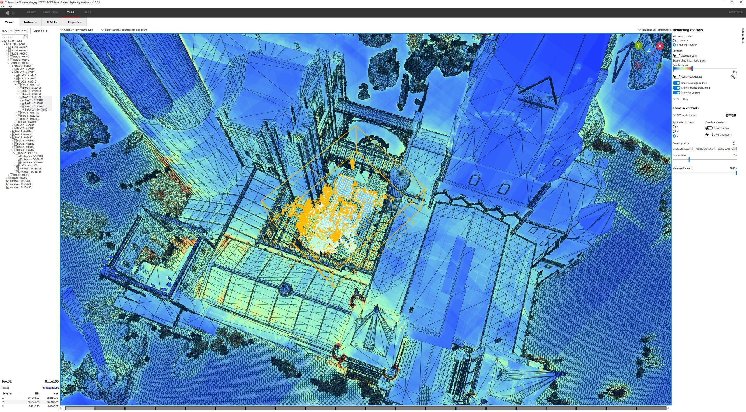
As with Cyberpunk, getting down to the bottom level involves quite a few hops. A Hogwarts student looking at the fountain is 13 levels in. Again, memory latency is going to be a distinct culprit because even hitting the L1 cache on RDNA 3 will cost 35 ns.
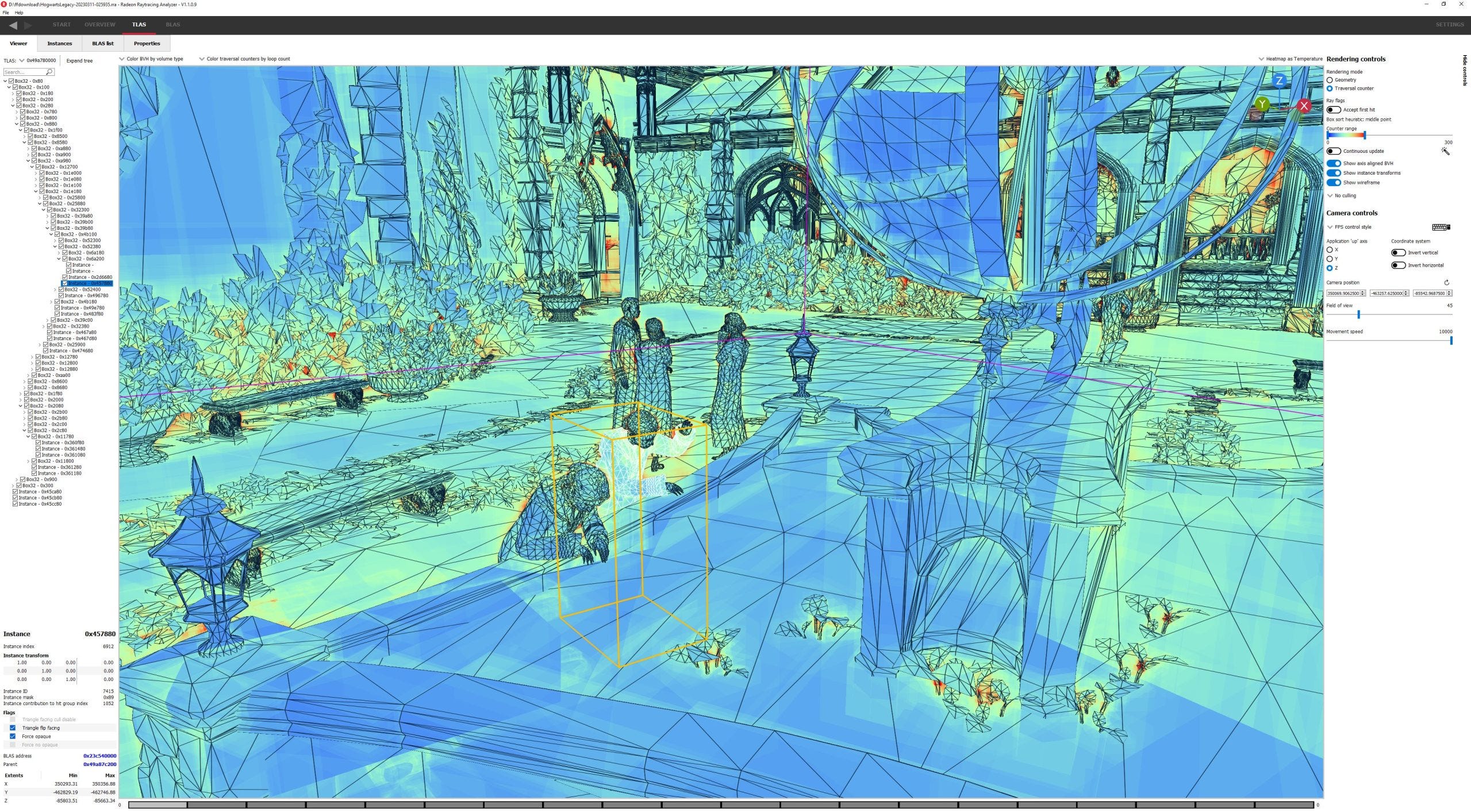
Curiously, the student’s (her?) body is represented by three BLAS-es. One represents most of her body. Another covers her hair, while yet another contains her face and hands.
The body BLAS is the largest, and goes down to very small subdivisions like parts of a button. I hope raytracing in this game looks incredible, because it takes 10 jumps to get to that part of a button.
This level of detail is not universal throughout the BVH. There’s also a cat in the courtyard, 12 levels down in the TLAS. A single BLAS represents the entire cat. Compared to the human BLAS-es, the cat BLAS is much simpler and represents an order of magnitude less geometry. It occupies 73 KB, and only has 196 box nodes covering a total of 460 triangles. It ends up being 6 levels deep on average, with a maximum depth of 9 levels.
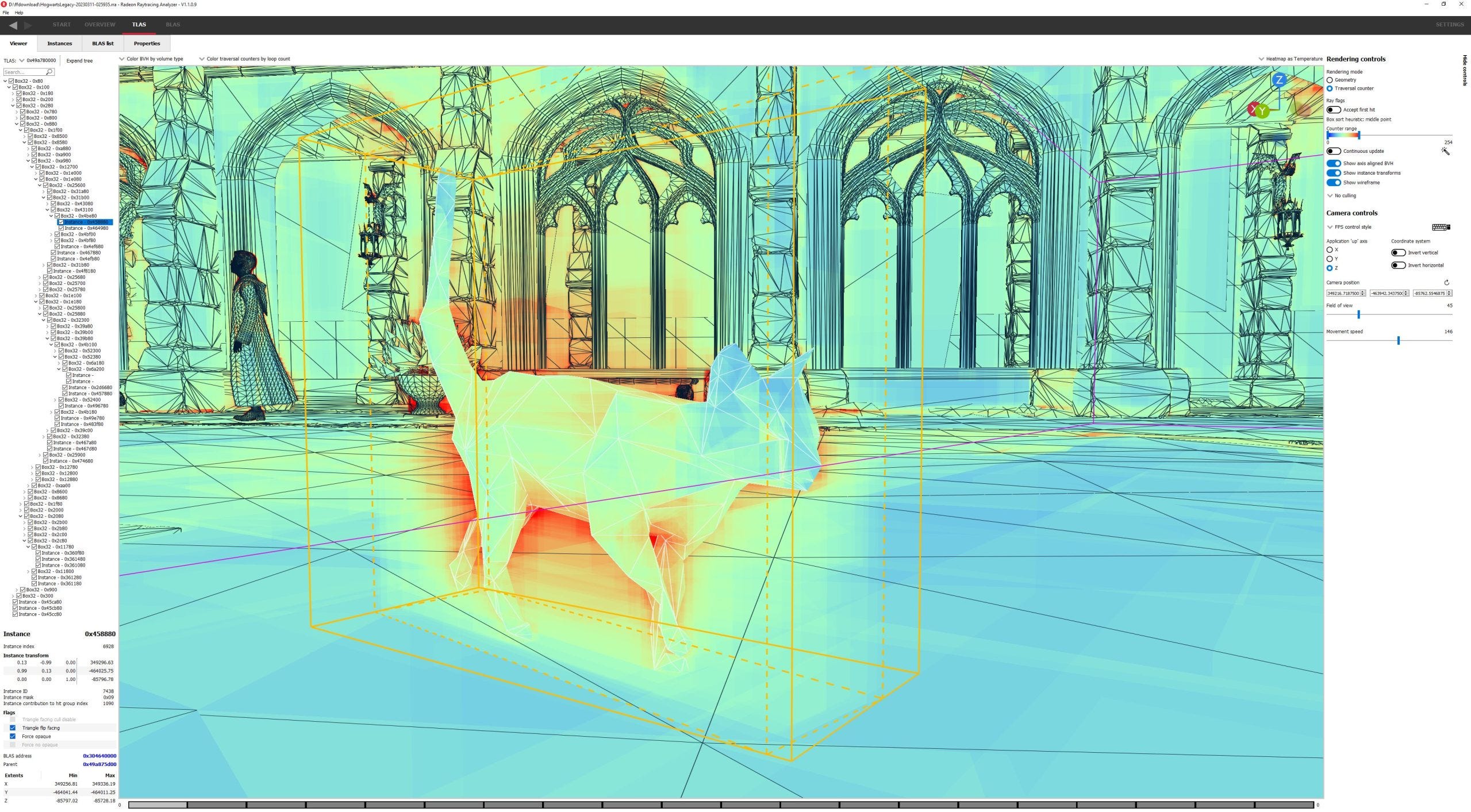
Clearly, the developers behind Hogwarts Legacy chose to optimize performance by deciding that cats are less important than humans.
Inline vs Indirect Raytracing
Microsoft’s DirectX raytracing API supports raytracing via two main methods. The first is inline raytracing, where one large shader program handles both traversing the BVH and performing the appropriate lighting calculations when it sees a rays hit or miss things. The second is indirect raytracing, where separate shader programs get invoked to handle ray hits and misses. This is a simplified explanation of course, so consider checking out Microsoft’s explanation of the API or Nvidia’s suggestions on what approach to use. But long story short, indirect raytracing suffers from the overhead of launching separate shader programs, while inline raytracing may suffer from a single shader program getting too big.
Cyberpunk 2077 uses inline raytracing, via DispatchRays<Unified> calls. Hogwarts Legacy, much like Unreal Engine 5’s city demo, uses indirect raytracing via ExecuteIndirect<Rays><Indirect> calls.

Indirect raytracing also gives us a pretty clear indication of raytracing costs. Ray traversal is the most expensive thing by far, but Hogwarts Legacy also spends quite some time handling hits once they’re found.
Nvidia’s Turing
Turing was Nvidia’s first architecture to implement hardware raytracing acceleration. With Turing’s launch, Nvidia made a significant investment both directly in raytracing acceleration, and in supporting technologies like DLSS. Since then, they’ve continued to double down on this area. It would be interesting to see whether Nvidia’s raytracing implementation has changed in their newer cards, but I don’t have an Ampere or Ada card. I happened to replace my GTX 1080 at the height of the cryptomining boom in 2021, and Ampere was ridiculously overpriced at the time. For sure RDNA 2 was overpriced too, just to a less ridiculous extent.

Nvidia did not document how the acceleration works at a low level, but we can at least examine the acceleration structures by using Nsight Graphics to take frame captures. The TLAS again covers the entire city, which isn’t a surprise because the application decides what the raytracing acceleration structures should cover. Just like AMD’s TLAS, Nvidia’s occupies about 11 MB.
However, Nvidia takes a very different approach to BVH construction. The way Nsight Graphics presents the BVH suggests it’s an extremely wide tree. Expanding the top node immediately reveals thousands of bounding boxes, each of which points to a BLAS. Each BLAS then contains anywhere from a few dozen to thousands of primitives. If Nsight’s representation corresponds to the actual raytracing structure, then Nvidia can get to the bottom of their acceleration structure in just three hops. That makes Nvidia’s implementation far less sensitive to cache and memory latency.
To enable this approach, Nvidia likely has more flexible hardware, or is handling a lot more work with the general purpose vector units. Unlike AMD, where nodes can only point to four children, Nvidia does not have fixed size nodes. One node can point to two triangle nodes, while another points to six. A single triangle node can contain hundreds of triangles.
However, this approach demands a lot more intersection test throughput. That’s actually a wise choice, because GPUs are designed to take advantage of tons of explicit parallelism. Unlike CPUs, latency optimizations are not critical, and that’s very visible in the memory hierarchy. L2 cache access on Nvidia generally go well over 100 ns. In the RTX 2060 Mobile’s case, L2 latency is around 120 to 143 ns, depending on whether you’re going through the TMUs.
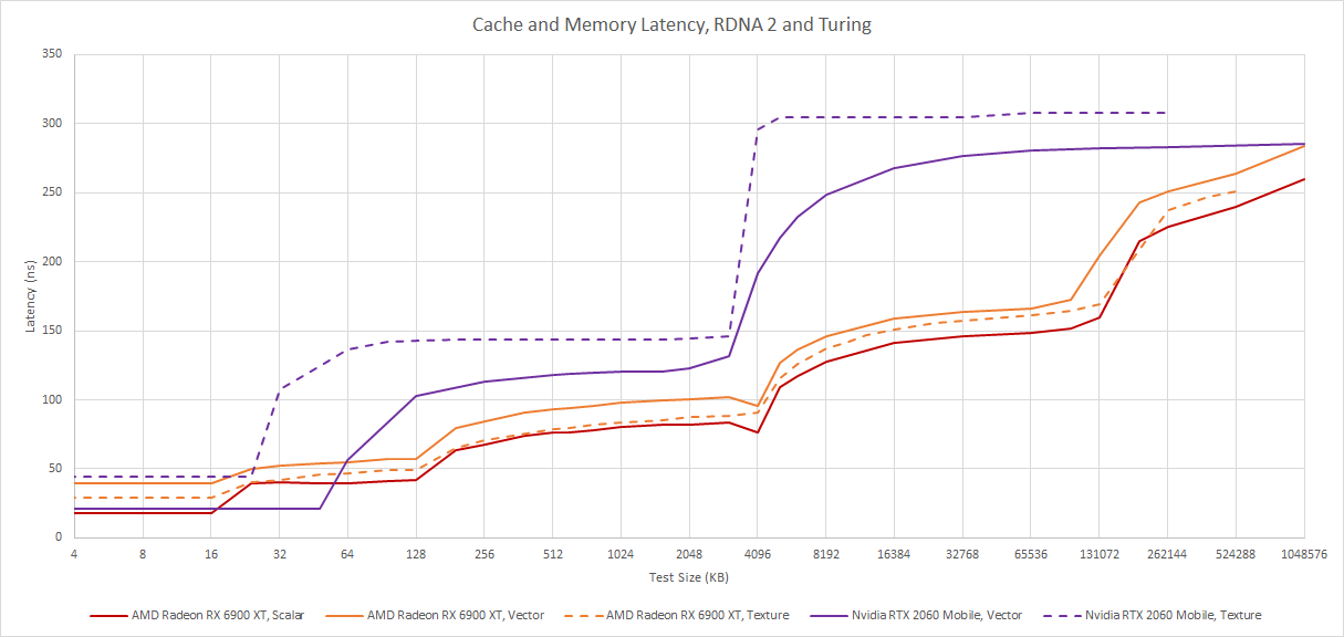
To counter that, Nvidia has a larger first level cache. But on Turing and many other Nvidia architectures, L1 and local memory (shared memory) are carved out of the same block of SRAM. Shared memory is Nvidia’s equivalent of AMD’s LDS, and both are great places to store a BVH traversal stack. There’s a chance that Nvidia won’t be able to maximize L1 cache sizes in raytracing workloads. Zooming into the longest DispatchRays call, we can see that Nvidia does achieve decent cache hitrates.

Turing’s L1 cache is large enough that it achieves better hitrate than AMD’s L1. That’s not surprising because Turing can still provide 24 KB of L1 capacity even when prioritizing shared memory. The 6900 XT in the example above got a cumulative L0 and L1 hitrate of 78.6%, so AMD’s mid-level L1 cache does help to even things out, but of course AMD’s L1 is technically a second level cache, and hitting it will be slower than hitting Nvidia’s first level cache. At L2, AMD has an advantage because the 6900 XT’s L2 is larger, and has lower latency. But that’s completely expected of a newer GPU with higher performance targets.
Turing’s basic building blocks are Streaming Multiprocessors, or SMs. They’re vaguely comparable to WGPs on AMD. However, Turing SMs are smaller than WGPs, and smaller than SMs on Pascal (the previous Nvidia generation). An RDNA 2 WGP or Pascal SM can keep 64 waves in flight, but a Turing SM can only track 32. In this DispatchRays call, Turing averaged an occupancy of 17.37 waves out of 32, or 54%. SM utilization was poor, with the execution ports active only 11.35% of the time.
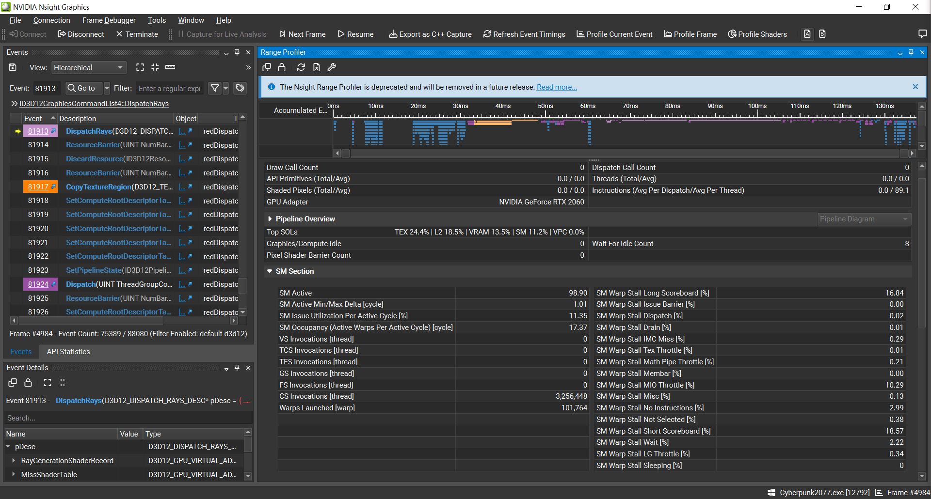
The biggest culprits are stalls for “short scoreboard” and “long scoreboard”. “Short scoreboard” refers to short duration, variable latency operations like shared memory access. Nvidia may be using shared memory to track BVH traversal state, so a good chunk of this is probably down to shared memory latency, which is around 15.57 ns on Turing. That’s pretty good compared to the regular caches, but still long in absolute terms.
“Long scoreboard” points to global memory latency. Global memory is backed by VRAM, and corresponds to what we think of as memory on a CPU. Ray traversal involves plenty of pointer chasing, so that’s not surprising. The third largest reason, “MIO throttle”, is harder to understand because it doesn’t point to a clear, single cause.
Warp was stalled waiting for the MIO (memory input/output) instruction queue to be not full. This stall reason is high in cases of extreme utilization of the MIO pipelines, which include special math instructions, dynamic branches, as well as shared memory instructions. When caused by shared memory accesses, trying to use fewer but wider loads can reduce pipeline pressure.
An Nvidia SM probably sends a variety of longer latency operations to a MIO queue. In this case, the RTX 2060’s SMs were occasionally bottlenecked by something behind that queue. It could be shared memory, special math instructions like inverse square roots or reciprocals, or even branches.

Another cause for poor SM utilization is that Turing’s SMs are just weaker in general. With Turing, Nvidia moved to statically split integer and floating point paths. For comparison, Pascal and RDNA can execute both integer and FP32 at full rate, and flexibly give execution bandwidth to whatever’s needed in the moment. In contrast, Turing will have to stall every other cycle if faced with a long sequence of FP32 instructions. To get the most out of Turing, you need a perfect mix of alternating INT32 and FP32 instructions. Maybe that didn’t happen.
Changes in Ampere
Looking at Turing’s struggles does help provide perspective on how Nvidia approached Ampere. First, they doubled the FP32 throughput in each SM. That should allow far better scheduler port utilization, because the SM no longer needs a perfect 1:1 ratio of INT32 to FP32 instructions to achieve peak throughput. In practice, FP32 instructions are far more common than INT32 ones, so this is a good move that should benefit a wide range of graphics applications beyond raytracing.
On the raytracing front, Ampere doubles the ray-triangle intersection test rate. This makes a lot of sense if Nvidia’s using a fat tree where triangle nodes can contain thousands of triangles. Such a strategy minimizes memory latency costs, but demands more intersection test throughput. Ampere’s change fits that. I have no doubt that Ampere is a far stronger architecture for both rasterization and raytracing than Turing.
Turing does have a rough time, but that’s really expected of a first generation raytracing implementation. No one buys the first generation of a new technology expecting anything more than a rough experience that gets rapidly outdated as technology matures. That applied to early digital cameras, early aircraft, and so on. Turing is no exception. But what’s important is that lessons learned with Turing informed major changes in Ampere, allowing Nvidia to create a very strong second generation raytracing implementation.
Nvidia’s Pascal
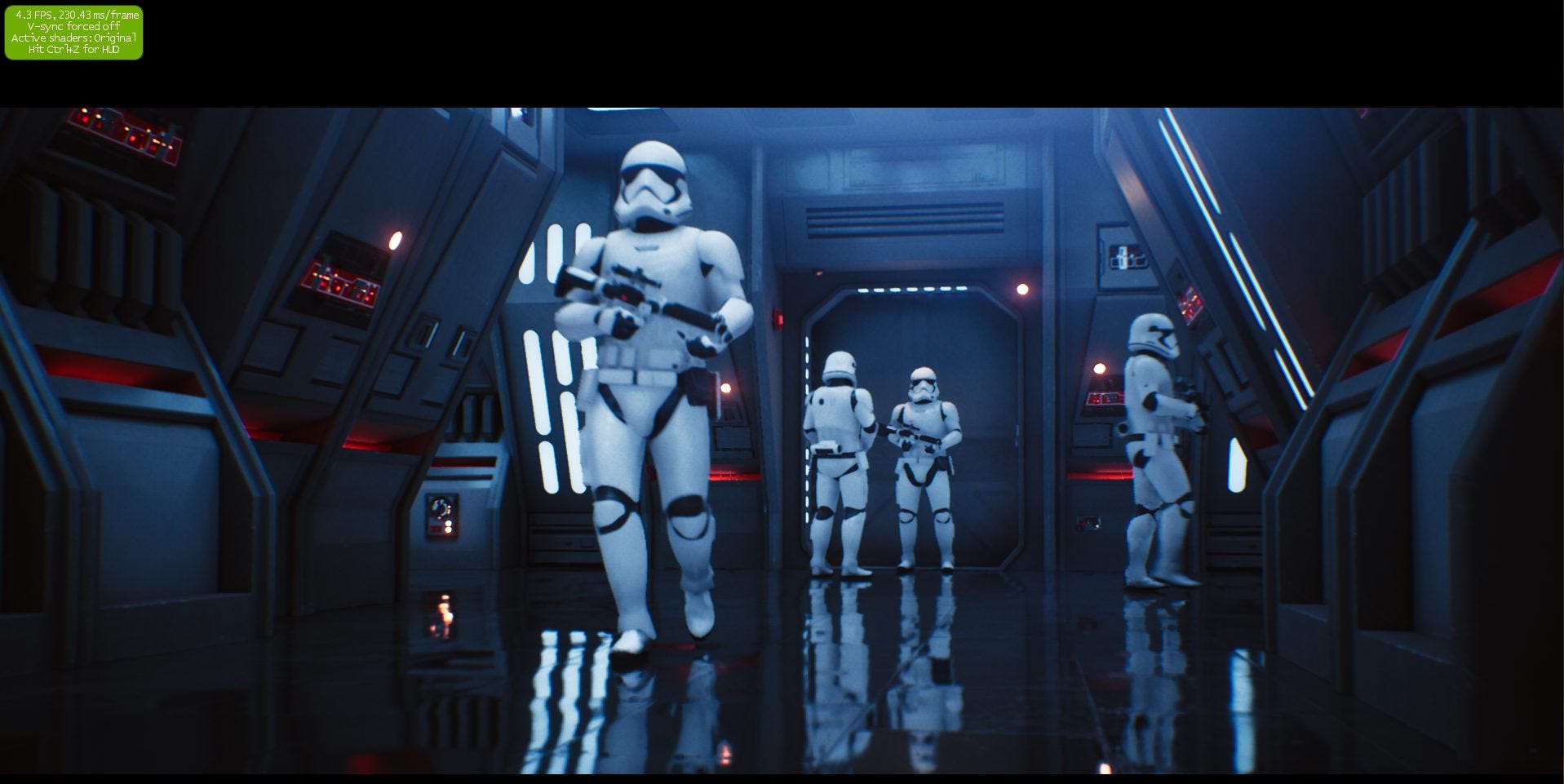
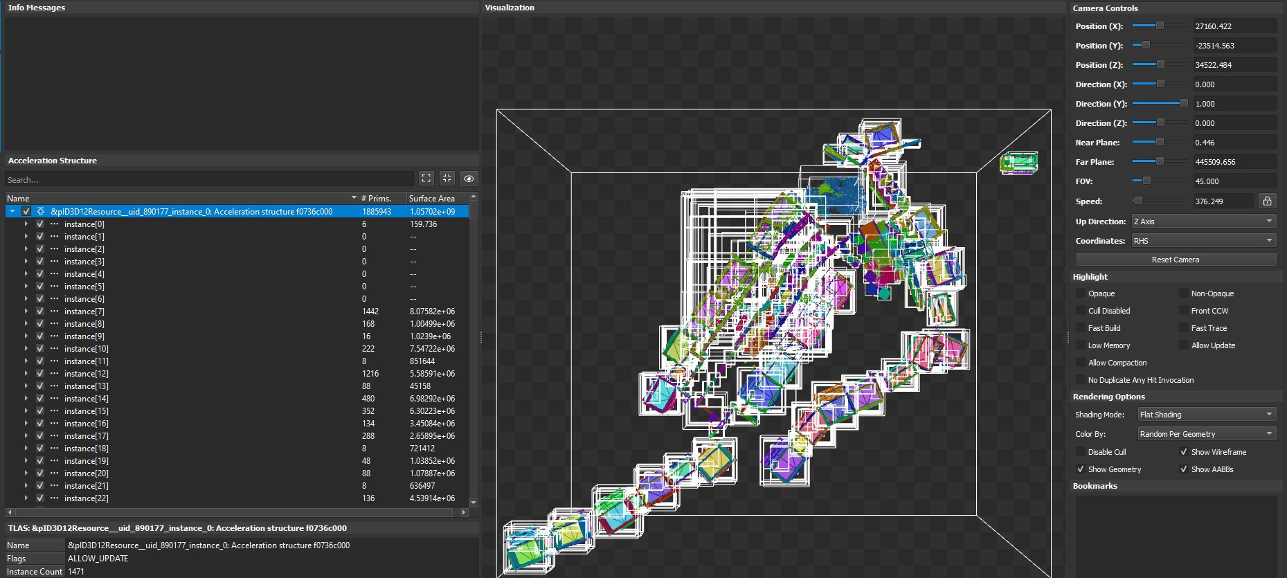
Nvidia’s Pascal architecture supports raytracing, but doesn’t have any specialized hardware to assist with raytracing. Instead, raytracing is done completely with compute shaders, using the same vector ALUs used to do traditional rasterization. I wasn’t able to profile Cyberpunk 2077 raytracing with Pascal, because the game says it’s not supported on the GTX 1080. Instead, I have some results from Nvidia’s RTX demos. I’m looking at the Star Wars demo specifically.
Like Turing, Pascal uses a very fat BVH. You can get from the root node to a triangle node in just three hops. Nvidia didn’t develop a separate raytracing strategy for Pascal, probably because all GPU raytracing implementations solve fundamentally similar problems, regardless of whether they have dedicated hardware to assist with raytracing. Pascal doesn’t have significantly different latency memory latency characteristics than Turing. Like any other GPU, Pascal is also optimized to take advantage of explicit parallelism in order to hide latency and feed a lot of vector execution units.
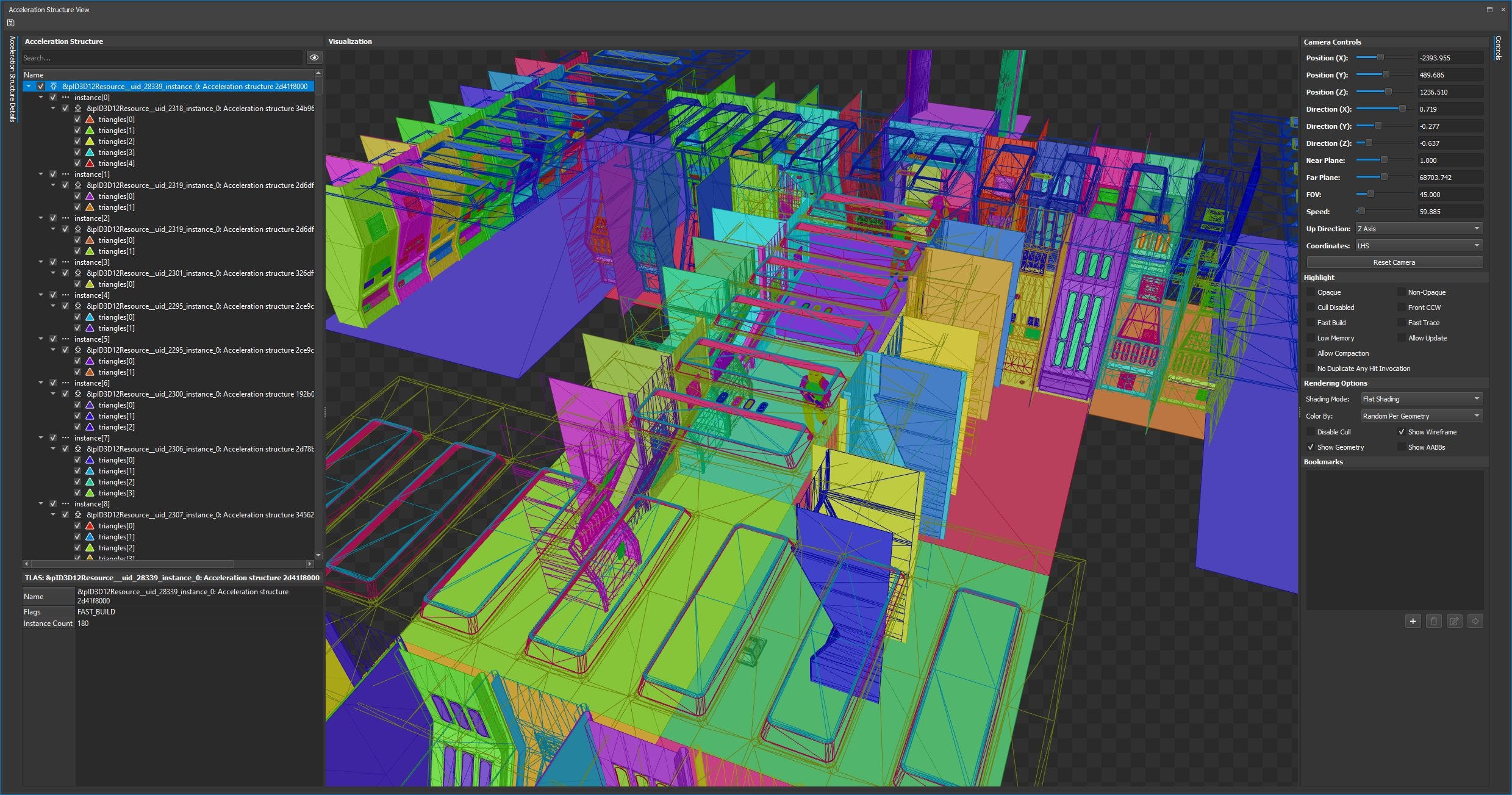
Again, we see raytracing acceleration structures cover just about everything. Unlike Cyberpunk and Hogwarts Legacy though, the total area covered is far smaller, because the demo is a lot smaller in scope. The TLAS consists of 180 instances, covering a total of 3,447,421 triangles. Because the demo is smaller in scope, Nvidia could afford to put a lot more detail into each object. The closest stormtrooper is represented by 555,698 triangles organized into 17 sub-boxes. Contrast that to Hogwarts Legacy, which represents a human with just over 8K triangles. Subdivisions on the stormtrooper go down to the visor on the helmet, the scope on the gun, and other minute details.
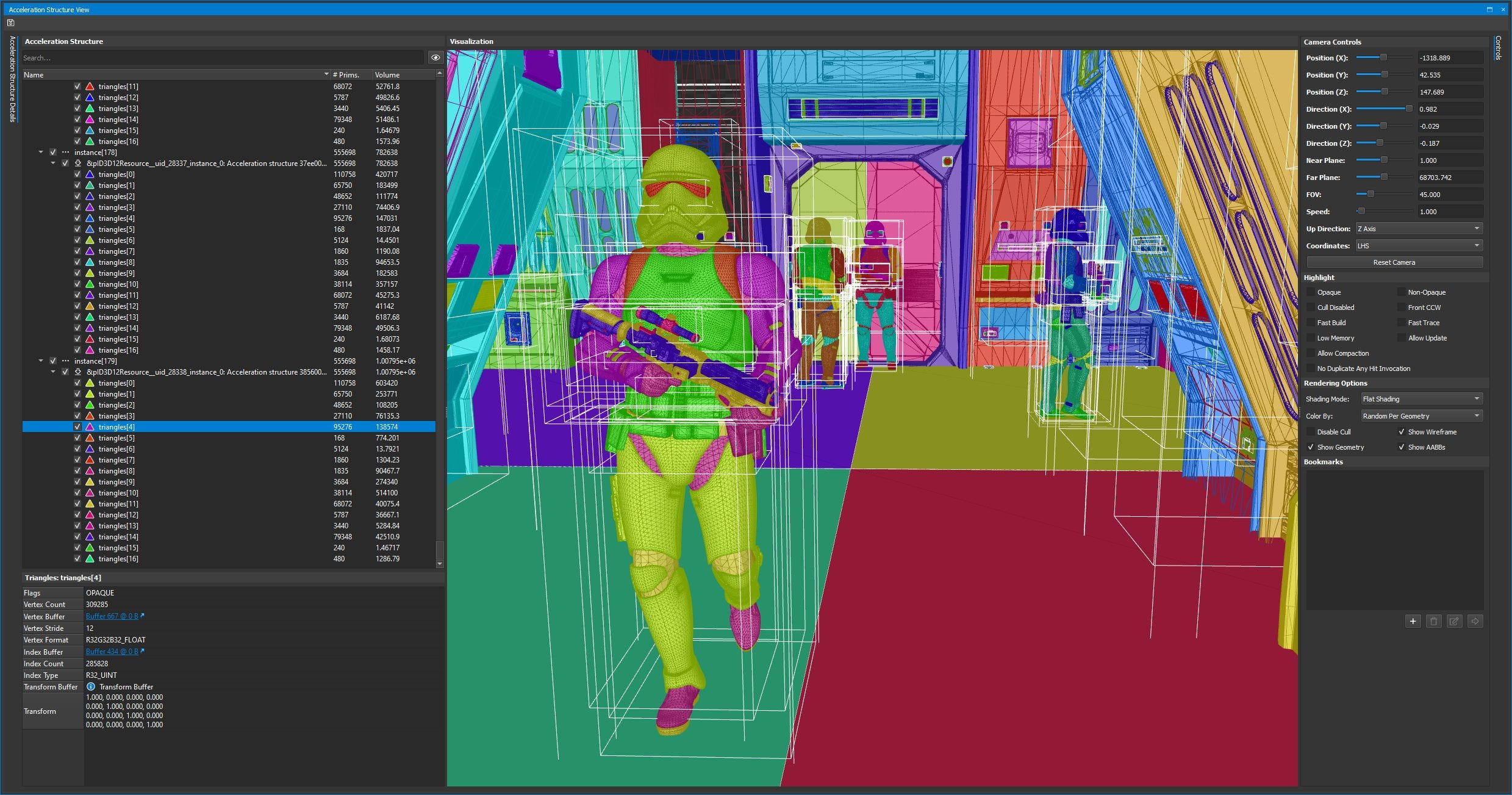
Compared to what we see in games, the stormtrooper has been lovingly modeled with a ridiculous amount of geometry, giving it very clean, rounded looking shape. Each of the stormtrooper’s triangle nodes has anywhere from a couple hundred to tens of thousands of triangles. Some nodes have even more triangles than the entire human in Hogwarts Legacy. For example, the helmet alone accounts for 110k triangles. This level of detail may be impossible to field in an open world game, but it’s fascinating to see in a scoped-down technical demo.

Pascal struggles hard to render this technical demo, with one DispatchRays call taking a staggering 26.72 ms. Each SM tracked 13.23 waves on average out of 64 theoretical, meaning that occupancy was very poor and the architecture couldn’t keep a lot of work in flight. A lot of warps were stalled on global memory latency (long scoreboard) just as with Turing, but a few other deficiencies show up too. There’s also a lot of stalling because of “no instructions” (instruction cache misses). Pascal suffers because it has smaller instruction caches relative to Turing, and because it has to do intersection tests without special instructions.
“Wait” is the third biggest stall reason, and points to instruction execution latency. Pascal has a latency of six cycles for the most common floating point and integer instructions, while Turing and Ampere bring that down to four cycles. The term “wait” is used because Nvidia handles instruction dependencies by embedding static scheduling info that tells the SM scheduler to stall a thread for a specified number of cycles. With low occupancy and plenty of stalling, Pascal’s SMs average just 1.09 IPC. According to Nsight, the SMs achieved about 22.3% of their theoretical efficiency. While that’s better than what Turing got in Cyberpunk 2077, Turing gets by because it’s throwing a lot of weaker SMs at the problem.
For sure, Pascal and Turing both suffer stalls due to shared memory, and it does look like Pascal’s doing a lot of shared memory accesses during raytracing. But on Pascal, that cost is peanuts compared to regular cache and memory latency.

The first culprit is Pascal’s L1 texture cache. Internally, a Pascal SM is partitioned into four SM sub partitions, which are analogous to a RDNA WGP’s SIMDs. Each pair of SMSPs share a memory pipeline and 24 KB L1 texture cache. While this cache is larger than RDNA’s L0 cache, hitrate is quite poor in this workload. On a L1 miss, we go straight to the L2, because there’s no mid-level cache to cushion the impact of first level cache misses.
Even on a L1 hit, Pascal is at a large disadvantage because there’s no way to bypass the texture units. The Pascal architecture is a lot less optimized for latency sensitive compute, and unfortunately raytracing is an example of that.

Once we get out to L2, Pascal does turn in a good performance. Pascal’s L2 has acceptable latency, and achieves good hitrates.
There’s also nuance to Pascal’s performance. Pascal’s SMs achieved very good throughput in the other two DispatchRays calls, where L1 hitrates were a bit higher. All of the calls pointed to the same BVH. Furthermore, Pascal achieved excellent compute utilization in the later RTReflectionFilter section.

So Pascal is capable of ripping through workloads with powerful vector units, using its dual issue capability to make sure the schedulers can feed the primary FP32 or INT32 pipes. However, the architecture suffers from low occupancy, likely due to its limited register file capacity and lack of separate scalar registers. Cache latency and instruction cache capacity also present problems. All of these were addressed to some extent in Turing, though at the cost of losing Pascal’s 32-wide vector units and dual issue capability.
Final Words
Raytracing is an exciting new area of development for graphics rendering. Tracing rays promises to deliver more accurate lighting effects with less work on the developer’s part. However, optimizing raytracing workloads is difficult. AMD and Nvidia both use acceleration structures that adopt a divide-and-conquer approach, but the two manufacturers differ a lot in just how they do the dividing.
AMD takes a more conventional approach that wouldn’t be out of place on a CPU, and uses a rigid BVH format that allows for simpler hardware. AMD’s RT accelerators don’t have to deal with variable length nodes. However, AMD BVH makes it more vulnerable to cache and memory latency, one of a GPU’s traditional weaknesses. RDNA 3 counters this by hitting the problem from all sides. Cache latency has gone down, while capacity has gone up. Raytracing specific LDS instructions help reduce latency within the shader that’s handling ray traversal. Finally, increased vector register file capacity lets each WGP hold state for more threads, letting it keep more rays in flight to hide latency. A lot of these optimizations will help a wide range of workloads beyond raytracing. It’s hard to see what wouldn’t benefit from higher occupancy and better caching.
Nvidia takes a radically different approach that plays to a GPU’s advantages. By using a very wide tree, Nvidia shifts emphasis away from cache and memory latency, and toward compute throughput. With Ada, that’s where I suspect Nvidia’s approach really starts to shine. Ampere already had a staggering SM count, with RT cores that have double the triangle test throughput compared to Turing. Ada pushes things further, with an even higher SM count and triangle test throughput doubled again. There’s a lot less divide and conquer in Nvidia’s approach, but there’s a lot more parallelism available. And Nvidia is bringing tons of dedicated hardware to plow through those intersection tests.
But that doesn’t mean Nvidia’s weak on the caching front either. Ada has an incredible cache hierarchy. I suspect Nvidia’s bringing that together with the factors above to stay roughly one generation ahead of AMD in raytracing workloads. With regards to raytracing strategy, and how exactly to implement a BVH, I don’t think there’s a fundamentally right or wrong approach. Nvidia and AMD have both made significant strides towards better raytracing performance. As raytracing gets wider adoption and more use though, we may see AMD’s designs trend towards bigger investments into raytracing.
If you like our articles and journalism, and you want to support us in our endeavors, then consider heading over to our Patreon or our PayPal if you want to toss a few bucks our way. If you would like to talk with the Chips and Cheese staff and the people behind the scenes, then consider joining our Discord.