
Microbenchmarking AMD’s RDNA 3 Graphics Architecture

Editor’s Note (6/14/2023): We have a new article that reevaluates the cache latency of Navi 31, so please refer to that article for some new latency data.
RDNA 3 represents the third iteration of AMD’s RDNA architecture, which replaces GCN in their consumer graphics lineup. At a high level, RDNA 3 aims to massively scale up compared to RDNA 2. The cache setup is tweaked at all levels to deliver increased bandwidth. To scale compute throughput beyond just adding more WGPs, AMD implemented dual issue capability for a subset of common instructions.
In this article, we’re going to do some microbenchmarking on a 7900XTX and look at differences compared to AMD’s RDNA 2 architecture. We’re also going to be incorporating results from Nemes’s GPU microbenchmarking suite. While I have decent coverage for CPU microbenchmarking, I haven’t been able to put nearly as much time into my OpenCL bsaed tests. Nemes has made excellent progress on her Vulkan-based GPU test suite, and her test provides better coverage in certain areas.
Memory Latency
Testing cache and memory latency gives us a good look at RDNA 3’s cache and memory setup. Latency testing is also complicated on post-GCN AMD graphics architectures, because the global memory hierarchy can be accessed through either the scalar or vector datapaths, which have different first level caches. If the compiler determines that a loaded value is constant across a wavefront, it can tell the GPU to use the scalar datapath. Because the scalar path is used for latency sensitive stuff like calculating memory addresses for a load across the wavefront, latency is quite decent (for a GPU). When accessing global memory AMD makes significant use of both the vector and scalar sides. The exact proportion will vary depending on workload, but generally, both are important.

Let’s start by looking at the scalar side. Like RDNA 2, RDNA 3 has a 16 KB, 4-way set associative scalar cache. Load-to-use latency for this cache is quite good at 15.4 ns for RDNA 3, and 17.4 ns for RDNA 2. RDNA 3 at least partially owes its latency advantage to higher clock speeds. Nvidia’s Ada Lovelace has slightly better latency when hitting the SM’s L1, which is impressive considering the size of Nvidia’s cache. We see 64 KB of L1 cache capacity here, but Ada Lovelace actually has a 128 KB block of SRAM that can be flexibly partitioned between L1 and shared memory (LDS) uses.
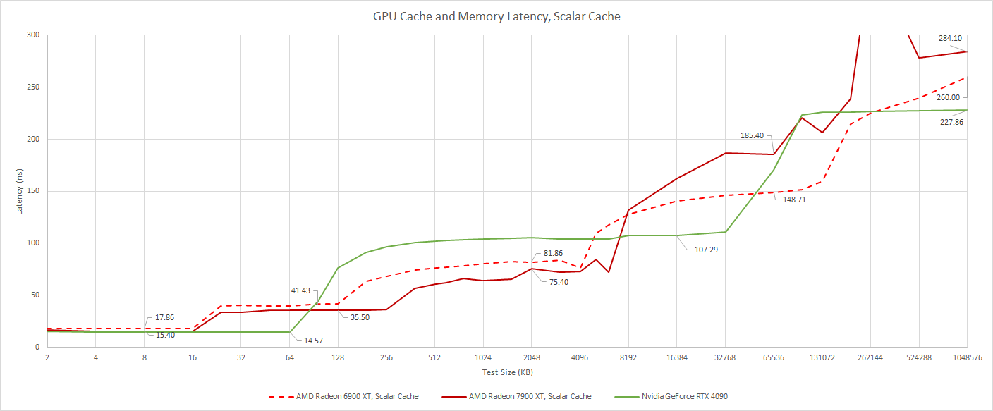
AMD also increased capacity in the L1 and L2 mid-level caches, in order to better handle the bandwidth demands from a larger GPU. RDNA 2 had a 128 KB, 16-way set associative L1 shared across a shader array. RDNA 3 doubles capacity to 256 KB, while maintaining 16-way associativity. L2 cache capacity increases to 6 MB, compared to 4 MB on RDNA 2, while also maintaining 16-way associativity. Despite these capacity increases, RDNA 3 delivers measurable latency improvements at both L1 and L2.
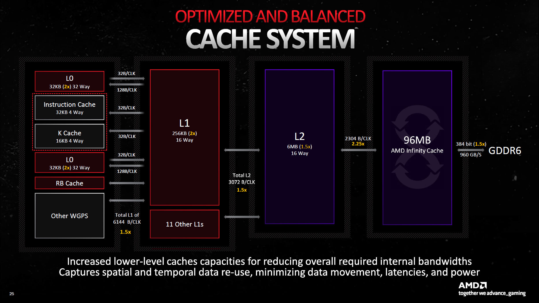
However, RDNA 3’s Infinity Cache regresses somewhat. Capacity decreases from 128 MB to 96 MB, and latency increases at the same time. That’s not surprising, because RDNA 3’s Infinity Cache is implemented on separate memory controller dies. But it also shouldn’t be a big deal. RDNA 3 will likely be able to service more memory accesses with its on-die L2, and not have to hit Infinity Cache as often.
To reduce memory bandwidth demands, Nvidia has chosen to massively scale up the L2 instead of adding another level of cache. That pushes up L2 latency a bit compared to AMD’s recent GPUs, but does give Ada Lovelace superior latency characteristics for memory footprints going into the dozens-of-megabytes range. The RTX 4090’s L2 has 72 MB of capacity, cut down from the 96 MB of SRAM physically present on the die.
VRAM latency is up slightly on RDNA 3 compared to RDNA 2. Nvidia holds an advantage in that area, partially because AMD incurs extra latency when they check an extra level of cache on the way to DRAM.
Vector Latency
Of course, latency for the vector path is important too, so I’ve modified the test to prevent the compiler from determining that the loaded value will be constant across the wavefront. Details are in another article. From the vector side, AMD sees increased latency, but vector accesses should be less latency sensitive. The vector cache’s design also plays a role – it’s 32-way set associative on both RDNA 2 and RDNA 3, compared to the 4-way scalar cache. Checking 32 tags on a lookup is probably going to incur higher latency than checking four.
Still, RDNA 3 manages to decrease L0 vector cache latency compared to RDNA 2, while doubling capacity to 32 KB per CU.
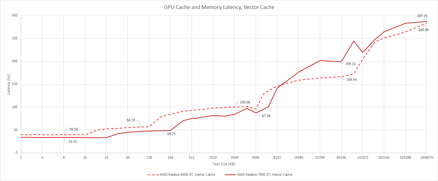
Further down the cache hierarchy, latency characteristics mostly mirror that of the scalar side, though of course absolute latencies are higher. RDNA 2’s VRAM latency advantage is also reduced when we test from the vector side. The two architectures end up a few nanoseconds off at the 1 GB test size, which is basically nothing.
Memory Bandwidth
The Radeon 7900 XTX has more WGPs than the 6900 XT. At the same time, each WGP has more compute throughput on tap, so the memory subsystem has to be beefed up to feed them. RDNA 3 therefore sees massive bandwidth increases at every level in the memory subsystem. The L1 and L2 caches see especially impressive gains, with bandwidth approximately doubling compared to RDNA 2 even though their capacity is also increased.

Infinity Cache bandwidth also sees a large increase. Using a pure read access pattern, we weren’t able to get the full 2.7x bandwidth increase that should be theoretically possible. Still, a 1.8x bandwidth boost is nothing to joke about. The bandwidth advantage is impressive considering the Infinity Cache is physically implemented on different chiplets, while RDNA 2 kept the Infinity Cache on-die.
AMD has also equipped the 7900XTX with a much larger GDDR6 setup, giving it a lot more bandwidth than the 6900XT. In fact, its VRAM bandwidth is a lot closer to GA102’s. That probably allowed AMD to maintain high performance while reducing the amount of last level cache, allowing for smaller memory controller dies.
Bandwidth at Lower Occupancy
Modern GPUs are built to take advantage of massive amounts of explicit parallelism. But some workloads don’t have enough parallelism to fill all available compute units. Vertex shaders, I’m looking at you. Nemes’s test suite currently doesn’t break out results for lower workgroup counts, so I’m using OpenCL results here.
Let’s start with bandwidth for a single workgroup. Running a single workgroup limits us to a single WGP on AMD, or a SM on Nvidia architectures. That’s the closest we can get to single core bandwidth on a CPU. Like single core bandwidth on a CPU, such a test isn’t particularly representative of any real world workload. But it does give us a look into the memory hierarchy from a single compute unit’s perspective.

Again, we can see RDNA 3’s larger on-die caches. From a single WGP’s point of view, all three of those cache levels offer increased bandwidth. Nvidia has a very large and fast first-level cache, but after that AMD has an advantage as long as it can serve accesses from L1 or L2.
From Infinity Cache, RDNA 3 has a harder time, likely because a single WGP didn’t get enough of an increase in memory level parallelism capabilities to absorb the increase in Infinity Cache latency. In fact, Infinity Cache bandwidth for one WGP has decreased compared to where it was in RDNA 2. The situation flips again when we hit VRAM, where RDNA 3 pulls ahead.
Bandwidth Scaling
Shared caches are nice because their capacity can be used more efficiently. Instead of duplicating shared data across several private caches, a shared cache can store the data once and service requests for it coming from multiple compute units. However, a shared cache is hard to implement, because it has to be able to handle the bandwidth demands of all of its clients.
We’re going to start with L2 bandwidth because L0 and L1 bandwidth scale almost linearly. L2 scaling is much harder to pull off because a single 6 MB L2 cache has to service all 48 WGPs on the GPU. With that in mind, RDNA 3’s L2 does a very good job with scaling to meet the bandwidth demands of all those WGPs. As WGP count increases, RDNA 3’s L2 bandwidth starts to pull away from RDNA 2’s.

Both AMD architectures are able to provide more L2 bandwidth to matched workgroup counts, compared to Nvidia’s Ada Lovelace. However, the RTX 4090 has larger first-level caches that should reduce L2 traffic. Ada Lovelace’s L2 also serves a slightly different role, doubling as an Infinity Cache of sorts. Considering its very large capacity, Nvidia’s L2 does extremely well. If we compare against RDNA 3’s Infinity Cache, which has similar capacity, Ada’s L2 maintains similar bandwidth at low occupancy. When all of Ada’s SMs come into play, Nvidia enjoys a substantial bandwidth advantage. Of course, AMD’s Infinity Cache doesn’t need to provide as much bandwidth because the L2 cache will often absorb a decent percentage of L1 miss traffic.

Compared to RDNA 2, RDNA 3’s Infinity Cache is a bit slower to ramp up, and is at a disadvantage with less than half of its WGPs loaded. But when workloads scale to fill all the WGPs, RDNA 3’s Infinity Cache shows a substantial bandwidth advantage over RDNA 2’s.

From VRAM, both AMD architectures enjoy very good bandwidth at low occupancy. RDNA 3 starts with a small advantage that gets larger as more WGPs come into play. From another perspective, RDNA 2’s 256-bit GDDR6 setup could be saturated with just 10 WGPs. RDNA 3’s bigger VRAM subsystem can feed more WGPs demanding full bandwidth. Nvidia has more trouble with VRAM bandwidth if only a few SMs are loaded, but takes a lead at higher occupancy.
Local Memory Latency
In addition to the regular global memory hierarchy, GPUs also have fast scratchpad memory. OpenCL calls this local memory. On AMD GPUs, the corresponding structure is called the Local Data Share (LDS). Nvidia GPUs call this Shared Memory. Unlike caches, software has to explicitly allocate and manage local memory capacity. Once data is in the LDS, software can expect guaranteed high bandwidth and low latency access to that data.
Like prior RDNA generations, each RDNA 3 WGP gets a 128 KB LDS. The LDS is internally built with two 64 KB blocks, each affiliated with one CU in the WGP. Each 64 KB block contains 32 banks, each of which can handle a 32-bit wide access. That makes it possible for the LDS to service a wavefront-wide load every cycle. We don’t currently have a test for LDS bandwidth, but RDNA 3 appears to have a very low latency LDS.

RDNA 3 makes a massive improvement in LDS latency, thanks to a combination of architectural improvements and higher clock speeds. Nvidia enjoyed a slight local memory latency lead over AMD’s architectures, but RDNA 3 changes that. Low LDS latency could be very helpful when RDNA 3 is dealing with raytracing, because the LDS is used to store the BVH traversal stack.
For comparison, RDNA 2’s LDS had about the same load-to-use latency as its scalar cache. It was still very useful because it could get data into vector registers a lot faster than was possible from the L0 vector cache. I checked the compiled code for this test, and it is using vector registers even though all but one thread in the workgroup is masked off.
WGP Compute Characteristics
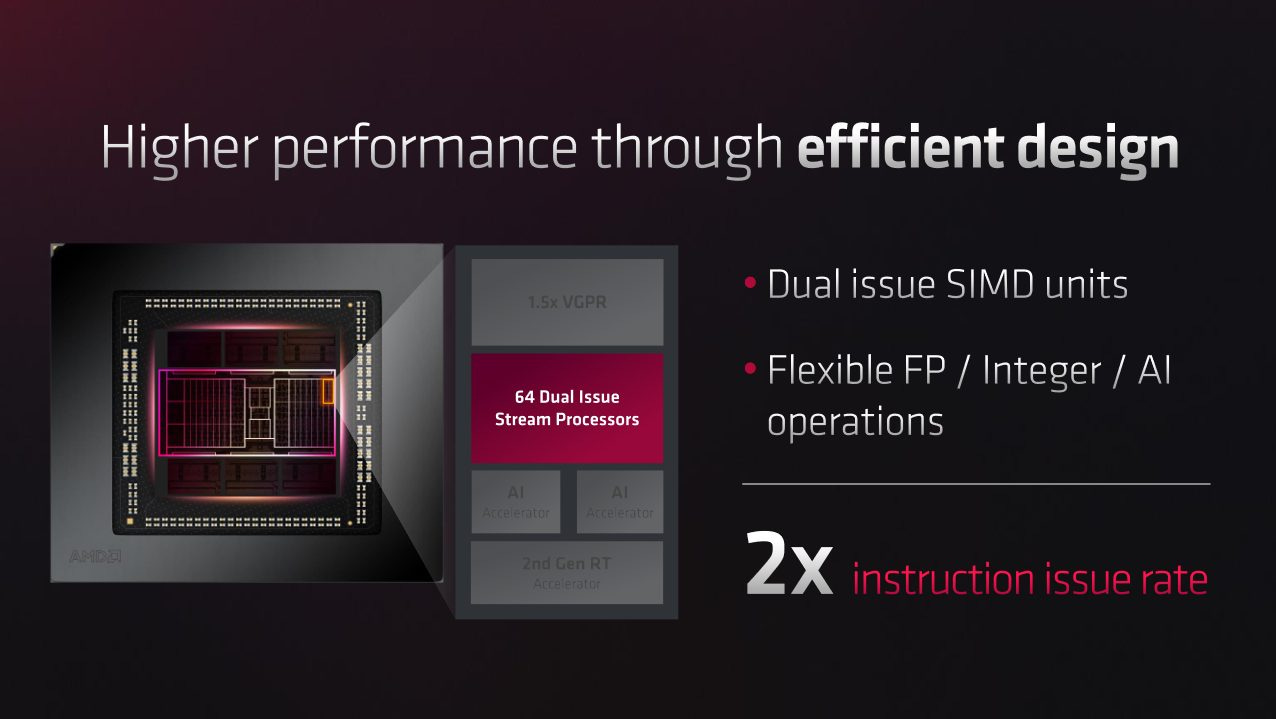
Compared to RDNA 2, RDNA 3 obviously has a large advantage in compute throughput. After all, it has a higher WGP count. But potential increases in compute throughput go beyond that, because RDNA 3’s SIMDs gain a limited dual issue capability. Certain common operations can be packaged into a single VOPD (vector operation, dual) instruction in wave32 mode. In wave64 mode, the SIMD will naturally try to start executing a 64-wide wavefront over a single cycle, provided the instruction can be dual issued.
A RDNA 3 VOPD instruction is encoded in eight bytes, and supports two sources and one destination for each of the two operations. That excludes operations that require three inputs, like the generic fused multiply add operation. Dual issue opportunities are further limited by available execution units, data dependencies, and register file bandwidth.
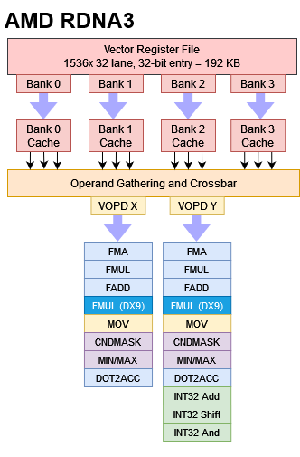
Operands in the same position can’t read from the same register bank. Earlier we speculated that this was a limitation with handling bank conflicts. However, AMD’s ISA manual clarifies that each bank actually has a register cache with three read ports, each of which is tied to an operand position. Two reads from the same bank in the same source position would oversubscribe the register cache ports. Another limitation applies to the destination registers, which can’t be both even or both odd.
In this test, we’re running a single workgroup to keep the test local to a WGP. Because boost behavior is quite variable on recent GPUs, we’re locking clocks to 1 GHz to drill down on per-clock behavior.

Unfortunately, testing through OpenCL is difficult because we’re relying on the compiler to find dual issue opportunities. We only see convincing dual issue behavior with FP32 adds, where the compiler emitted v_dual_add_f32 instructions. The mixed INT32 and FP32 addition test saw some benefit because the FP32 adds were dual issued, but could not generate VOPD instructions for INT32 due to a lack of VOPD instructions for INT32 operations. Fused multiply add, which is used to calculate a GPU’s headline TFLOPs number, saw very few dual issue instructions emitted. Both architectures can execute 16-bit operations at double rate, though that’s unrelated to RDNA 3’s new dual issue capability. Rather, 16-bit instructions benefit from a single operation issued in packed-math mode. In other major categories, throughput remains largely similar to RDNA 2.

I’m guessing RDNA 3’s dual issue mode will have limited impact. It relies heavily on the compiler to find VOPD possibilities, and compilers are frustratingly stupid at seeing very simple optimizations. For example, the FMA test above uses one variable for two of the inputs, which should make it possible for the compiler to meet dual issue constraints. But obviously, the compiler didn’t make it happen. We also tested with clpeak, and see similar behavior there. Even when the compiler is able to emit VOPD instructions, performance will only improve if compute throughput is a bottleneck, rather than memory performance.
On the other hand, VOPD does leave potential for improvement. AMD can optimize games by replacing known shaders with hand-optimized assembly instead of relying on compiler code generation. Humans will be much better at seeing dual issue opportunities than a compiler can ever hope to. Wave64 mode is another opportunity. On RDNA 2, AMD seems to compile a lot of pixel shaders down to wave64 mode, where dual issue can happen without any scheduling or register allocation smarts from the compiler.
It’ll be interesting to see how RDNA 3 performs once AMD has more time to optimize for the architecture, but they’re definitely justified in not advertising VOPD dual issue capability as extra shaders. Typically, GPU manufacturers use shader count to describe how many FP32 operations their GPUs can complete per cycle. In theory, VOPD would double FP32 throughput per WGP with very little hardware overhead besides the extra execution units. But it does so by pushing heavy scheduling responsibility to the compiler. AMD is probably aware that compiler technology is not up to the task, and will not get there anytime soon.
In terms of instruction latency, RDNA 3 is similar to prior RDNA architectures. Common FP operations execute with 5 cycle latency. Nvidia has a slight edge here, and is able to execute common operations with 4 cycle latency.

Since Turing, Nvidia also achieves very good integer multiplication performance. Integer multiplication appears to be extremely rare in shader code, and AMD doesn’t seem to have optimized for it. 32-bit integer multiplication executes at around a quarter of FP32 rate, and latency is pretty high too.
Full GPU Throughput – Vulkan
Here, we’re using Nemes’s GPU benchmark suite to test full GPU throughput, which takes into account boost clocks with all WGPs active. RDNA 3 achieves higher throughput via VOPD instructions, higher WGP count, and higher clock speeds. Strangely, AMD’s compiler is very willing to transform Nemes’s test code sequence into VOPD instructions.

The result is a massive increase in FP32 throughput. FP16 sees a smaller throughput increase because RDNA 2 is able to use packed FP16 execution, with instructions like v_pk_add_f16. Those instructions interpret each 32-bit register as two 16-bit elements, doubling throughput. RDNA 3 does the same, but is not able to dual issue such packed instructions. Curiously, RDNA 3 actually regresses in FP64 throughput. We already saw a hint of this earlier with OpenCL, where one RDNA 2 WGP could execute eight FP64 operations per cycle. RDNA 3 cuts throughput in half, meaning a WGP can do four FP64 operations – probably one per SIMD, per cycle.
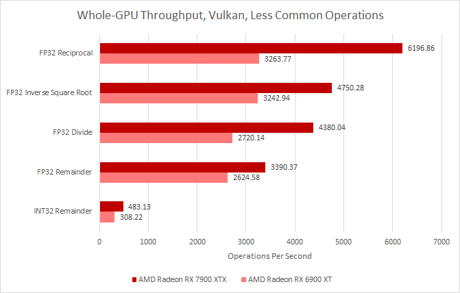
Throughput for special operations is lower on both GPUs. Reciprocal is often used as a way to avoid expensive division operations, and that runs at quarter rate on both architectures. Divide is even slower, and doing modular arithmetic on integer operations is about as slow as doing FP64.
Now, lets talk about that 123TFLOP FP16 number that AMD claims. While this is technically correct, there are significant limitations on this number. Looking at the RDNA3 ISA documentation, there is only one VOPD instruction that can dual issue packed FP16 instructions along with another that can work with packed BF16 numbers.

This means that the headline 123TF FP16 number will only be seen in very limited scenarios, mainly in AI and ML workloads although gaming has started to use FP16 more often.
PCIe Link
The Radeon 7900 XTX connects to the host via a PCIe 4.0 x16 link. Like RDNA 2, AMD’s new graphics architecture performs very well when moving data to the GPU, especially in moderately sized blocks. Transfer rate is lower when getting data off the GPU.

Nvidia lands somewhere in the middle, with decent transfer speeds across all copy sizes and directions. At large copy sizes, Nvidia seems to have an edge in PCIe transfer bandwidth over AMD.
Kernel Launch Latency
Here, we’re using clpeak to estimate how long it takes for a GPU to launch a kernel and report its completion. Clpeak does this by submitting a very tiny amount of work to the GPU and testing how long it takes to complete.
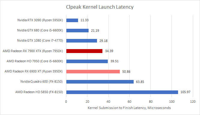
Results seem to vary quite a bit, and we can’t match platforms with our testing model. However, we can tell that there’s nothing out of the ordinary with RDNA 3. Nvidia might have slightly faster kernel launches on their GPUs, but since we couldn’t match platforms, it’ll be hard to draw any conclusions.
Final Words
AMD’s RDNA 2 architecture brought the company’s GPUs within striking range of Nvidia’s best, marking another instance in which AMD lands within striking distance of Nvidia’s highest end cards. RDNA 3 looks to carry that forward by scaling up RDNA 2, while introducing architectural improvements aimed at increasing performance beyond just adding WGPs. AMD employs a multi-pronged strategy in pursuit of that goal.
On the physical implementation side, AMD moved to TSMC’s more modern 5 nm process node. 5 nm allows for higher transistor density, and improvements to the WGP without bloating area. So, the WGP gets increased register file size and dual issue capability. Chiplet technology allows for a smaller main 5 nm die, by moving Infinity Cache and memory controllers onto separate dies. That helps enable a higher bandwidth VRAM setup by using less area on the graphics die to implement VRAM connectivity.
Higher bandwidth is key to feeding a larger GPU, and AMD goes beyond VRAM bandwidth. Caches bandwidth increases at every level. AMD has also increased capacity for on-die caches, because off-die accesses are more power hungry even with an interposer between dies. Even with a chiplet setup, AMD needs to maximize area efficiency, and dual issue is an excellent example of that. VOPD instructions allow AMD to add extra execution units for the most common operations, but with very little extra overhead in other places. AMD also increased vector register file capacity, which should help improve occupancy. And, they dramatically reduced LDS latency. Raytracing seems like an obvious beneficiary of that change.
The result is a GPU that performs very closely to Nvidia’s RTX 4080. According to Hardware Unboxed, the 7900 XTX is 1% slower at 1440p, and 1% faster at 4K. Instead of using a very large WGP/SM count, AMD achieved their performance by improving per-WGP throughput. They also focused on keeping the WGPs fed with a more sophisticated memory hierarchy. Total last level cache capacity drops compared to the previous generation, because the 384-bit memory bus means RDNA 3 doesn’t need as high of a cache hitrate to avoid bandwidth bottlenecks.

AMD and Nvidia thus make different tradeoffs to reach the same performance level. A chiplet setup helps AMD use less die area in a leading process node than Nvidia, by putting their cache and memory controllers on separate 6 nm dies. In exchange, AMD has to pay for a more expensive packaging solution, because plain on-package traces would do poorly at handling the high bandwidth requirements of a GPU.
Nvidia puts everything on a single larger die on a cutting edge 4 nm node. That leaves the 4080 with less VRAM bandwidth and less cache than the 7900 XTX. Their transistor density is technically lower than AMD’s, but that’s because Nvidia’s higher SM count means they have more control logic compared to register files and FMA units. Fewer execution units per SM means Ada Lovelace will have an easier time keeping those execution units fed. Nvidia also has an advantage with their simpler cache hierarchy, which still provides a decent amount of caching capacity.
In any case, it’s great to see AMD and Nvidia continuing to compete head to head after years of Nvidia having an unquestioned lead. Hopefully, that’ll lead to lower GPU prices in the future, as well as more innovation from both sides.
If you like our articles and journalism and you want to support us in our endeavors then consider heading over to our Patreon or our PayPal if you want to toss a few bucks our way or if you would like to talk with the Chips and Cheese staff and the people behind the scenes then consider joining our Discord.
What's up with the dismally poor dual issue rate? Back in the VLIW5 days, AMD had an average packing rate of 3.4. With RDNA3, I get the impression using that second ALU is like shooting for the moon. The four read ports would restrict dual FMA operations, but I assume it's more than that.