Golden Cove’s Lopsided Vector Register File
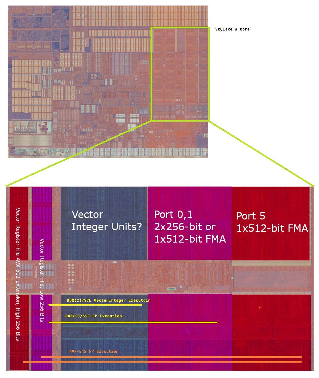
Ever since Intel first brought AVX-512 to their big core lineup, they made all of the vector registers 512-bit. They extended the vector register file on the opposite side of the execution units, and used that extension to store the upper 256 bits of a 512-bit vector register. The low 256 bits were kept in the same place, in prime real estate close to the execution units. That arrangement made sense because instructions that work on 512-bit vectors were going to be rare, especially when AVX-512 first released.

Keeping the more commonly used low bits closer to the execution units helped Intel optimize those operations for low power and high frequency operation. However, 512-bit operations are at a disadvantage. 512-bit floating point operations were especially disadvantaged, because the extra FP units on server CPUs were implemented as an extension to the core. They were placed on the opposite side of the main execution units, putting them quite far away from the register file they’d have to get their inputs from. This might have contributed to low clock rates and high power consumption on early server AVX-512 implementations. Gradually, Intel reduced that penalty with a better process node and better architecture design.
But those improvements competed against the need to improve reordering capacity for out of order execution. Out of order execution lets a CPU temporarily skip past a long latency instruction and keep looking for independent instructions to execute. Letting a CPU buffer more instructions and reach further ahead improves performance. Reaching farther ahead before stalling (more reordering capacity) also helps compensate for increased cache latency, because the longest latency instructions are usually cache misses.
That in turn demands larger register files, because you need registers to store results for in-flight instructions. AVX-512 registers are especially difficult both because of their distance from certain execution units, and the large amount of data being moved.

To balance these competing demands, Golden Cove makes a sacrifice on AVX-512 renaming capacity. On Golden Cove, the AVX-512 register file extension doesn’t cover all of the vector registers. From a performance perspective, that means only a subset of Golden Cove’s vector registers are 512-bit. Physically, that’s visible on the die shot too. Prior AVX-512 capable Intel architectures had the same number of blocks in both portions of the register file. However, Golden Cove has notably fewer blocks in the AVX-512 extension part. We can use microbenchmarks to estimate how register file capacity is distributed.
Golden Cove has approximately 295 renames for 256-bit vector registers, but only 210 for 512-bit ones. If we assume that 32 registers are used to hold architectural state across both SMT threads, that gives 242 physical registers with 512-bit capacity out of 327 total. Compared to Ice Lake, Golden Cove provides more registers in both categories, but will see the biggest improvements for AVX(2) and SSE code.
Interestingly, we see full register file capacity when alternating between instructions that write to 256-bit and 512-bit registers. Golden Cove is mostly using the non-512-bit capable registers to track the 256-bit results, reserving the 512-bit capable ones for results that need their full width. Golden Cove’s renamer is apparently very sophisticated. It’s probably tracking two separate pools of vector registers and using heuristics to determine whether a 256-bit result should be stored in a 512-bit capable register.
What About HyperThreading?
Modern high performance CPUs from both Intel and AMD use SMT, where a core can run multiple threads to make more efficient use of various core resources. Ironically, a large motivation behind SMT is likely the need to improve single threaded performance. Doing so involves targeting higher performance per clock with wider and deeper cores. But scaling width and reordering capacity runs into increasingly diminishing returns. SMT is a way to counter those diminishing returns by giving each thread fewer resources that it can make better use of. SMT also introduces complexity because resources may have to be distributed between multiple active threads.
Golden Cove’s vector register file is also lopsided in terms of how entries are divided up between active threads. If you load both threads in a core, you expect each to get about half of the register file capacity. That’s how it was done in early Intel SMT implementations, like in Netburst and Sandy Bridge. But Golden Cove can give significantly more than half of its vector registers to a single thread, even when the sibling thread is out of halt state. We can test this by loading the sibling thread with a dummy workload that doesn’t touch the FP/vector registers at all.
Intel is likely using a watermarking scheme in Golden Cove, meaning that one thread is not allowed to use more than a certain number of entries (high water mark) when two threads are active. One thread can only use up to 221 FP registers for renaming, or 141 registers for 512-bit operations.
We can also conduct a slightly different experiment where we load both threads up with the structure size microbenchmark. That means both threads are competing for vector register file capacity. In this case, it looks like one thread is guaranteed to get at least 130 SSE/AVX registers, or at least 106 AVX-512 vector registers. The high water mark appears to be the same. Between these two points, there’s a region where the thread has some probability of getting the entries it needs to parallelize the two long latency loads in this microbenchmark.
Golden Cove is not the first Intel CPU to use such a watermarking scheme for the vector register file. Ice Lake SP shows signs of this too, so this feature was probably introduced in the previous generation. Skylake seems to cut the vector register file perfectly in two. Anyway, yet another optimization Intel has done to increase die area efficiency and SMT yield, while guaranteeing some level of fairness between two threads sharing a core.
What About AMD?
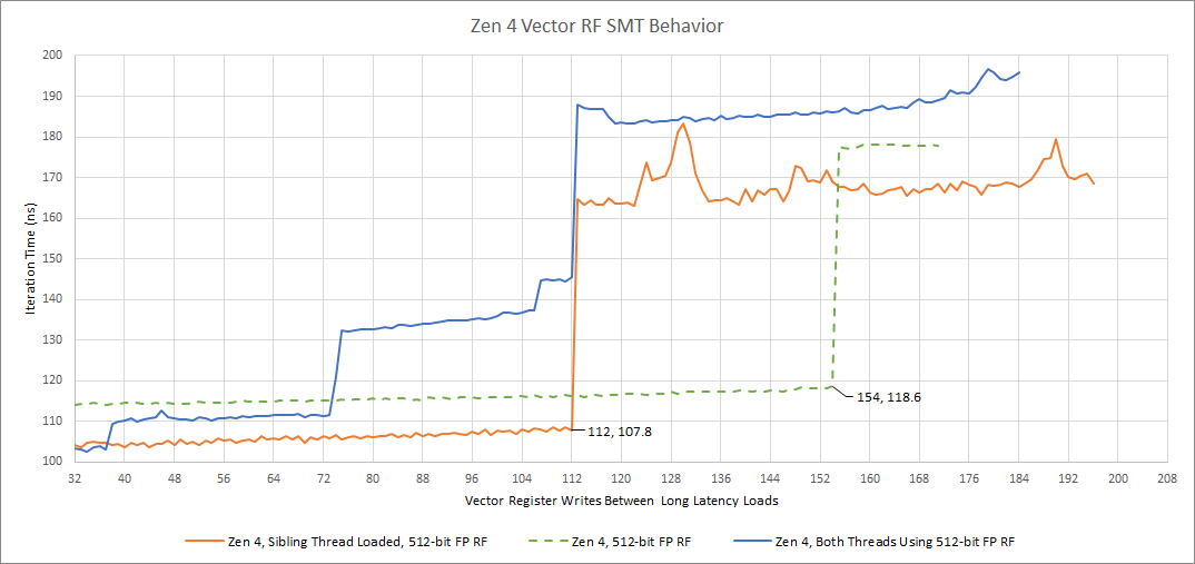
Zen 4 has the same renaming capacity regardless of whether instructions are writing to 256-bit or 512-bit registers. Physical layout has actually changed compared to prior Zen generations, putting the execution units on one side of the register file. Previously, AMD reduced critical path lengths by placing execution units on both sides of the registers, at the expense of moving the registers a bit farther away from the load/store unit. That makes Zen 4’s FP dataflow look a bit like Intel’s.

However, Zen 4 has much less difficult problem to solve. It has fewer vector registers to begin with, meaning that data doesn’t have to travel as far because the register file’s physical size is smaller. The vector execution units are also smaller, especially compared to server Intel CPUs, because AMD has generally not built more expensive FP execution units since Zen 2.
With regards to SMT register allocation, AMD appears to competitively share the vector register file. There is no cut-in-half partitioning or watermarking. One thread can use a very large portion of the vector register file even when the second thread is active. The difference in reordering capacity when a second thread comes active but doesn’t use FP registers, is accounted for by having to store architectural state for the second thread. That’s 32 AVX-512 registers and eight MMX/x87 registers. Other than that, the first thread is free to use whatever it needs from the vector register file. Zen 2 appears to use a similar strategy, though of course fewer registers are reserved to hold architectural state because AVX2 only has 16 vector registers.
Final Words
Intel has made some important changes to their vector register file in the past couple generations, and those changes have largely flown under the radar. However, I find those optimizations to be very interesting, and a sign that Intel is putting a lot more effort into efficiently using die area than most people probably realize.
SMT yield is improved by watermarking, letting Intel claw back more area efficiency after using massive structures to absorb cache latency. Not giving all the vector registers full 512-bit width lets Intel increase performance for more common client and server workloads. It’s also an acknowledgement that AVX-512 will continue to serve a limited role for the next few generations.
Still, Golden Cove continues to have a very impressive AVX-512 implementation. Renaming capacity for 512-bit registers still improves over Ice Lake SP, and both generations of Intel CPUs can bring more registers to bear than Zen 4 can. And getting such a system working well is a testament to the engineering muscle Intel can bring to the table, even after years of suffering from process node issues.
Of course, none of this is particularly relevant for Golden Cove. AVX-512 won’t be accessible on the architecture for most customers. We had to use a chip that didn’t have AVX-512 fused off and an old BIOS that allowed enabling AVX-512 to do this testing. However, we do wonder whether Sapphire Rapids will show similar behavior. We have very strong reasons to believe it does.
If you like our articles and journalism and you want to support us in our endeavors then consider heading over to our Patreon or our PayPal if you want to toss a few bucks our way or if you would like to talk with the Chips and Cheese staff and the people behind the scenes then consider joining our Discord.


