
Cannon Lake: Intel’s Forgotten Generation

Palm Cove (also commonly known as Cannon Lake) is Intel’s 10 nm die shrink of the Skylake core. In Intel’s “Tick Tock” strategy of alternating major microarchitecture changes and ports to new process nodes, Palm Cove was meant to be the “Tick” following Skylake. By the time Palm Cove became available in 2018 in the form of Cannon Lake-U, it was already late. Skylake had been refreshed in Kaby Lake form. Much like the “Devil’s Canyon” refresh of Haswell, Kaby Lake was basically Skylake pushed to higher clock speeds, and was meant to serve as a stopgap until Palm Cove was ready.
Unfortunately for Intel, its 10 nm process struggled. Cannon Lake, which uses Palm Cove cores, wound up being the first in a long line of 10 nm products that never got a full launch across Intel’s lineup. Cannon Lake’s launch was particularly limited because it appeared in just a single SKU. The Core i3-8121U offered a 2 core, 4 thread Palm Cove configuration with a 15W power target, and boosted up to 3.2 GHz. Thanks to cha0s, we have microbenchmark results run on the i3-8121U. And thanks to FritzchensFritz, the same chip got decapped and photographed. We’ll be using data from both in this article.
To keep things clear, we’ll refer to each CPU in play using two names, the SoCs name and the CPU core architecture name. Here’s how to keep up:

As expected for a die shrink, Palm Cove is largely similar to Skylake. Therefore, we’ll focus on the major differences in this article. The most obvious difference is the process node, so we’ll start with that.
The Process: Face Palm Cove?
Intel’s 10 nm process was supposed to replace 14 nm, and offered much higher density. Up to this point, Intel held a commanding process advantage over its competitors, and exploited that to leave AMD in the dust. 10 nm was supposed to continue this trend, allowing Intel to ward off any competition with ease.
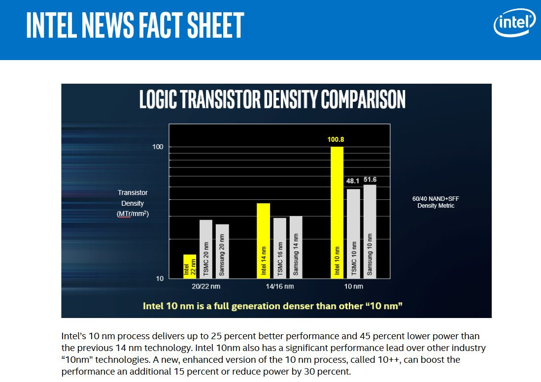
Intel’s news briefings before 2018 suggest that they wanted 10 nm to make a gigantic leap over 14 nm and provide much higher density than other 10 nm offerings. Palm Cove is unique because it’s the first core launched on 10nm, and should give us a look into 10 nm’s early days. Let’s start by testing libx264 video encoding. This should be a best case scenario for Palm Cove, because libx264 can take advantage of AVX-512.
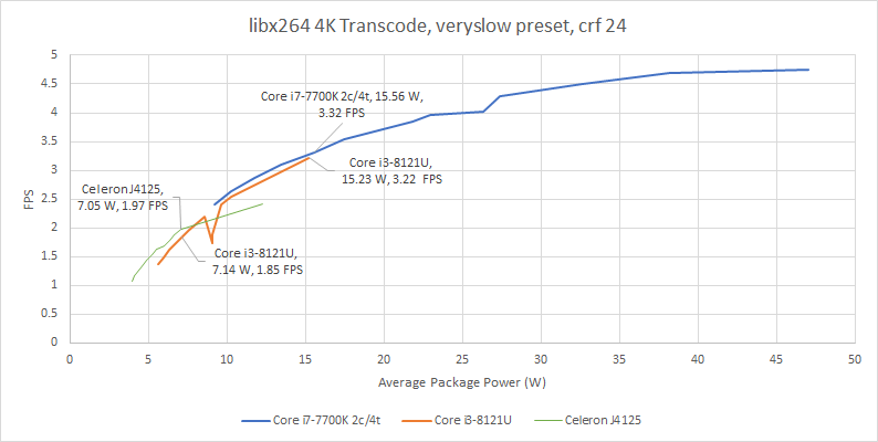
If we look at package power counters, early 10 nm is a disaster. Process node shrinks usually deliver significant improvements at low to moderate power targets, especially in the FinFET era. Usually, we see small gains in maximum performance as well. 10 nm delivers none of that. In overlapping power ranges, Kaby Lake delivers better performance on 14 nm, even with the test locked via affinity to two cores and four threads. Against Goldmont Plus, a low power Atom-class architecture also implemented on 14 nm, Palm Cove only pulls ahead at higher power targets within the ultrabook range. That potentially makes Goldmont Plus a better choice for very power constrained form factors, like tablets. We used Goldmont Plus in the form of the Celeron J4125, codenamed Gemini Lake.
I suspect something’s funny about Kaby Lake’s power counters, since non-core power ends averaging just above 1W throughout most of the test points. Cannon Lakes’s non-core power is around 3-4 W, while Gemini Lake’s is around 2-3 W. I don’t believe that Kaby Lake’s uncore draws just above 1 W, when Skylake’s uncore regularly pulls 6 W under load.
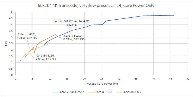
10 nm looks better if we focus on core power. There, Palm Cove draws roughly 10% less power to deliver similar performance. But that’s still not a good result, because a good chunk of that could come from AVX-512 advantages. AVX-512 lets the core finish a given amount of work using fewer instructions, and that usually results in lower instructions per clock and higher performance per clock. That in turn should give an AVX-512 enabled CPU an edge when those instructions are in play.
At lower power levels, Palm Cove still fails to beat Goldmont Plus at very low power targets, which is especially disappointing. Goldmont Plus only supports SSE and doesn’t even have a particularly strong SSE implementation, so it should have been utterly destroyed at similar power levels.
Now, let’s look at 7-Zip, a pure integer workload. Here, we’re compressing a 2.67 GB file. AVX-512 doesn’t come into play, making it a bit more of a fair process node comparison, instead of an architecture comparison. Again, looking at the package power counter does Cannon Lake no favors.

Cannon Lake does slightly better against Gemini Lake, and stays ahead as long as you’re running above 7 W. But it’s still not the kind of knockout blow I’d expect a new process node to land. Again, core power paints a better picture. But without an AVX-512 advantage, Palm Cove falls behind.

This is a devastating result for 10 nm, and suggests Palm Cove’s earlier advantage in libx264 is more due to AVX-512 than the 10 nm process node. Kaby Lake is simply better at the same power levels, and can scale to hit higher performance and power targets too.
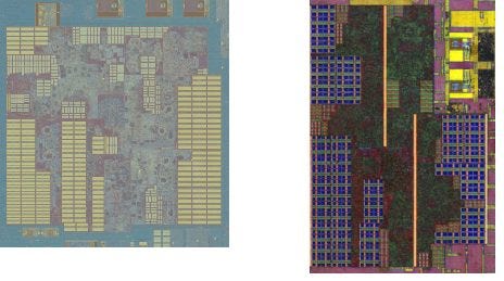
On the bright side, FritzchensFritz’s die photo shows that Intel’s 10 nm node did offer large density improvements over 14 nm:
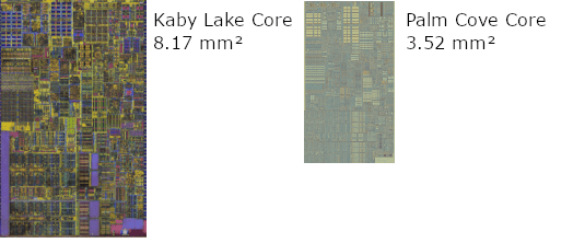
In line with its name, which probably refers to smacking something with the palm of your hand in an attempt to make it smaller, Palm Cove is tiny compared to Kaby Lake. It occupies just 43% of the area. While 10 nm’s density improvements likely gave Intel enough transistor budget to support AVX-512 on Palm Cove, it unfortunately didn’t provide the performance per watt uplift that we expect from process node shrinks. Intel therefore kept using 14 nm parts to fill out its lineup.
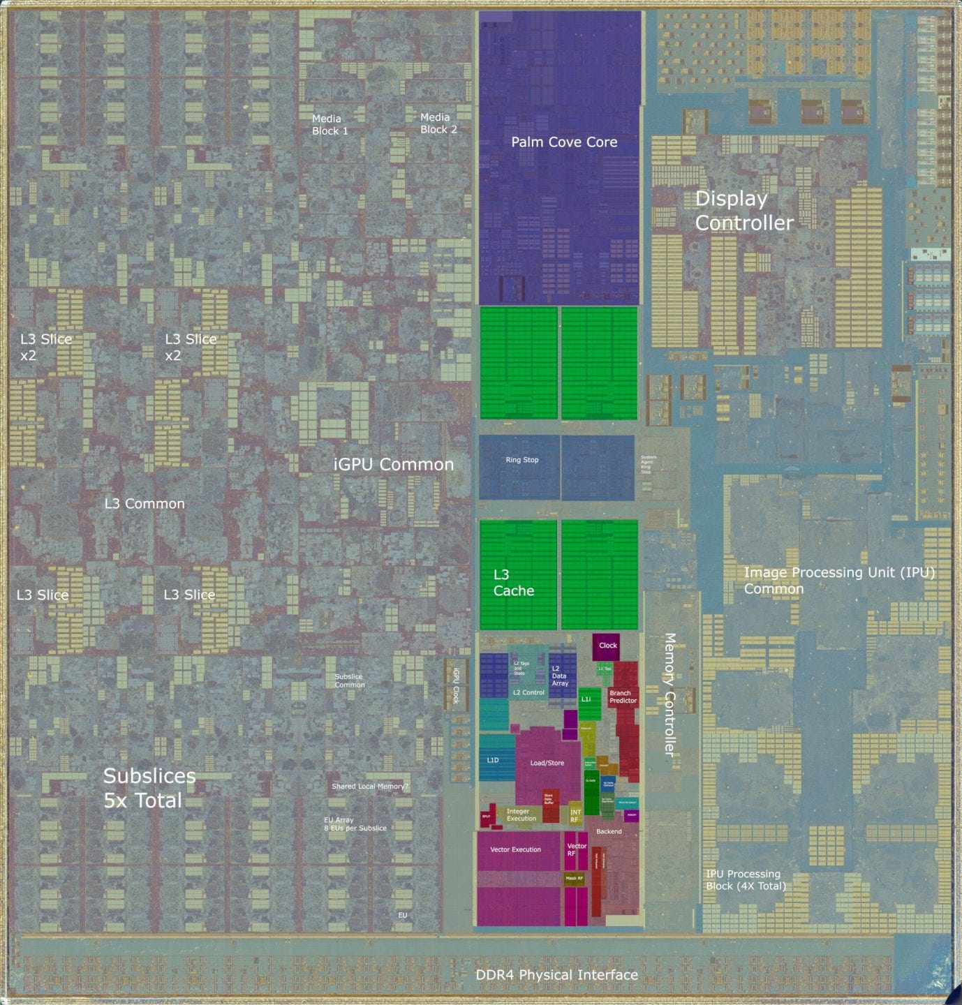
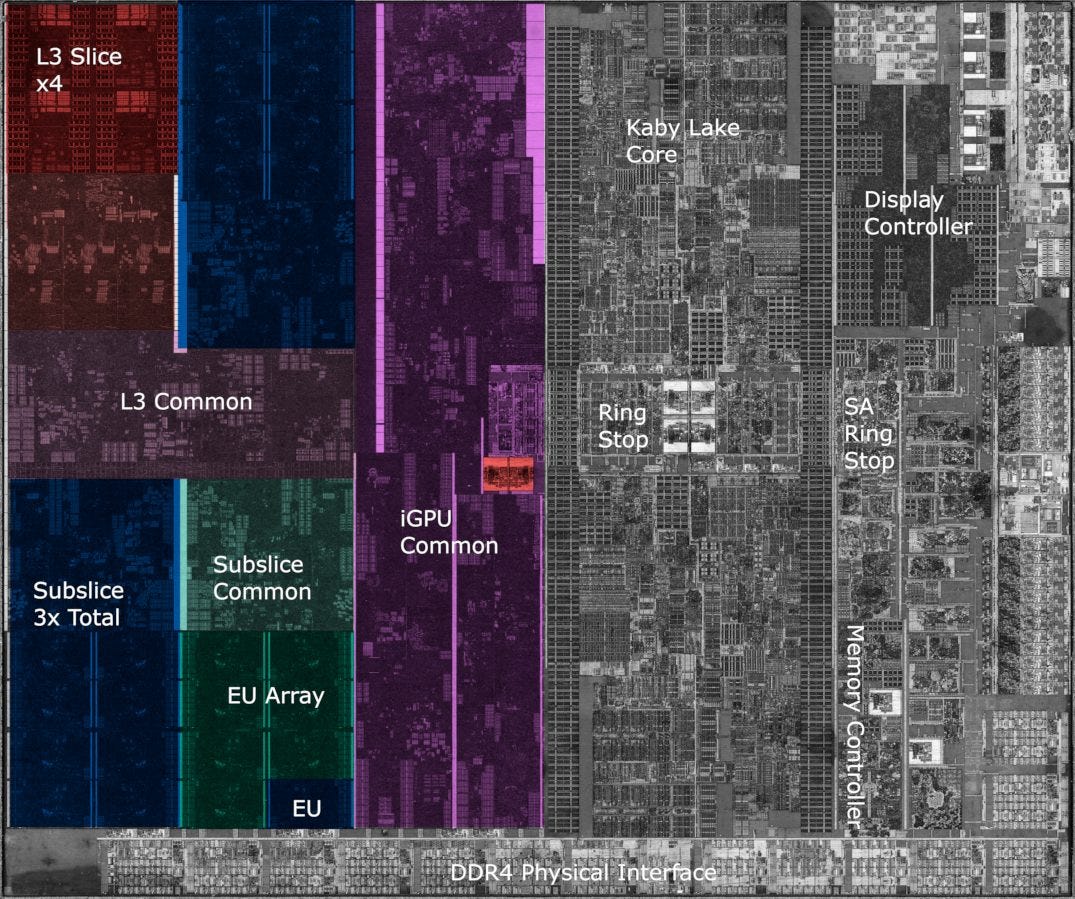
Now, let’s have a look at Cannon Lake, starting with the CPU cores. The CPU cores, their ring bus stops, and L3 cache take up just over 16% of die area.
Minor Core Changes
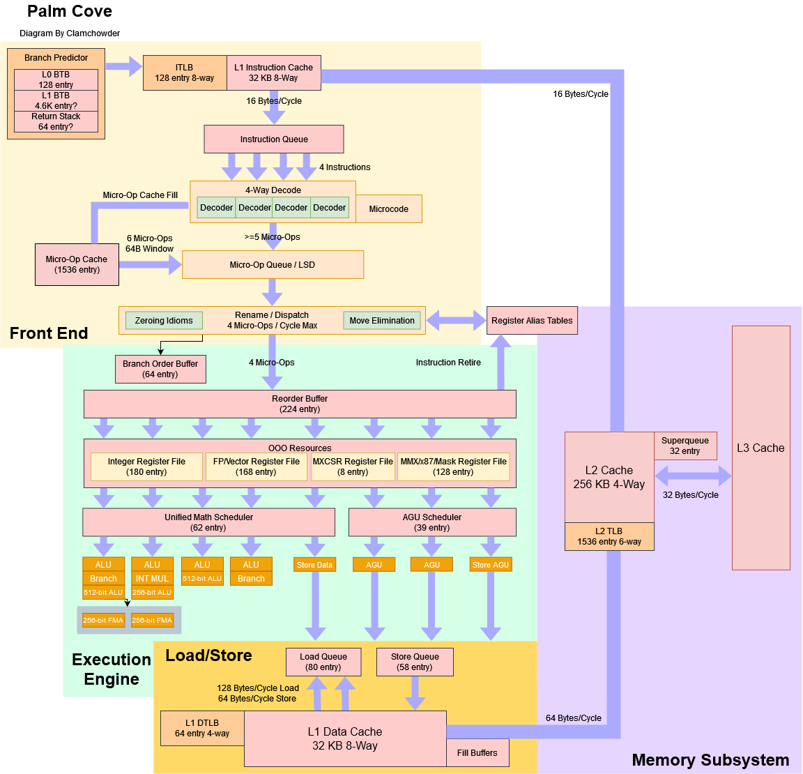
Intel’s “Tick Tock” strategy aims to reduce risk by avoiding major architectural changes while moving to a new process node. Palm Cove mostly follows that philosophy, but Intel did make a few more changes to core structures. Specifically, the math scheduler gains a few entries, going from 58 entries on Skylake to 62 on Palm Cove. The load/store unit also gets bigger queues. Palm Cove can now track 80 loads pending retirement, while Skylake could only track 72. Intel also increased the store queue size from 56 to 58 entries.
These are pretty minor changes, and their impact on performance will probably be barely measurable. Still, they indicate Intel was aiming somewhat higher than with prior process node shrinks, where structure sizes didn’t see any change at all.
Branch Predictor Improvements
Palm Cove’s branch target buffer (BTB) setup is very similar to Skylake’s, though the BTB may have gotten a slight size increase. Skylake’s BTB seems to be 4096 entries in size, but Palm Cove was able to track 4608 branches when they were spaced by 32 bytes. Like Skylake, taken branches can be handled with zero bubbles as long as they’re spaced by at least 32 bytes, and fit within a 128 entry tracking structure. Targets fetched from the main BTB incur a 1 cycle penalty, which also mirrors Skylake’s behavior.

Skylake’s BTB implementation slightly regressed compared to Haswell’s and required rather loose branch spacing to take full advantage of its zero-bubble taken branch capabilities. Palm Cove doesn’t fully solve that, but improves zero-bubble behavior when branches are spaced by less than 32 bytes:

When BTB capacity is exceeded, Palm Cove also shows a slower increase in taken branch penalties, and seems to hit an inflection point at around 8K branches. Perhaps the BTB replacement policy has been changed to be non-LRU, which means that hitrate gradually decreases as branch count exceeds BTB capacity. When tons of branches are in play and BTB capacity is nowhere near enough, both Palm Cove and Skylake can complete a taken branch every 9 cycles.
AVX-512 Implementation and Vector Execution
AVX-512 support is one of Palm Cove’s most significant improvements over client Skylake. Client Skylake lacked AVX-512 support, even though provisions were made to support AVX-512 in the server version. 10 nm likely gave Intel the transistor density to bring AVX-512 into a client SKU (Cannon Lake). Palm Cove therefore stands out as the first Intel client architecture with AVX-512 support. However, Palm Cove still makes some sacrifices to reduce AVX-512 implementation cost. Unlike server Skylake, there’s no FPU extension to 2×512-bit, meaning that theoretical floating point throughput remains identical to client Skylake’s. However, just about everything else was left in place.

Palm Cove’s FP execution layout is particularly interesting, because it fuses the existing FMA setup to handle 512-bit operations. Theoretically, there’s enough FP execution width to handle an even mix of 256-bit and 512-bit FMA instructions at something above 1 IPC. Centaur’s CNS similarly combines two 256-bit execution units for 512-bit FMA, and does exactly that. AMD’s Zen 4 does the same.
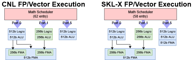
However, Palm Cove executes the test at 1 IPC. We see that dispatching a 512-bit FMA operation blocks sending another FMA operation down port 1, as that would obviously oversubscribe the execution units. But for some reason, the execution engine can’t alternate between 1×512-bit and 2×256-bit mode. My theory is that Palm Cove can either set up its FMA units to act as one 512-bit unit or as 2×256-bit as in client Skylake, but cannot have both modes active at same time. To explain:

This limitation might apply to server Intel CPUs equipped with two 512-bit FMA units. If we feed a 2:1 mix of 256-bit FMA and 512-bit FMA operations to Skylake-X, we are stuck at 2 IPC. Perfect scheduling would provide 3 IPC, by sending two 256-bit FMA instructions down ports 0 and 1, while sending one 512-bit FMA instruction down port 5. However, it seems like Skylake-X and Ice Lake X are not able to schedule operations in this way. Luckily, this throughput limitation doesn’t matter for vector integer instructions. Palm Cove features a full width 512-bit integer unit on port 5. If we mix 256-bit or 512-bit integer instructions with 512-bit FMA operations, we get well over 1 IPC.
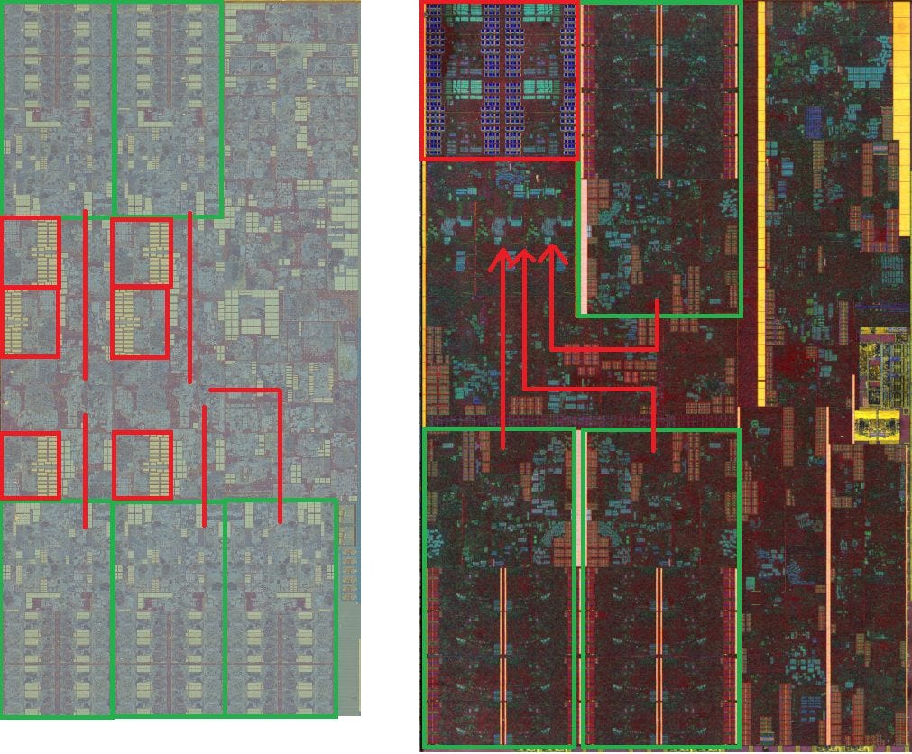
Thanks to Fritzchens Fritz, we have high resolution die shots that we can annotate to illustrate Palm Cove’s vector execution. With 256-bit operations, the vector execution unit probably operates something like this:
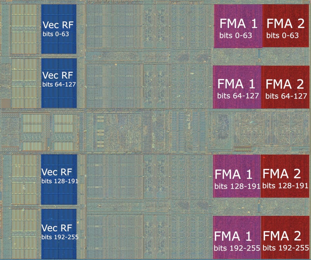
With 512-bit operations, the FMA units on ports 0 and 1 are fused, creating a configuration like this:
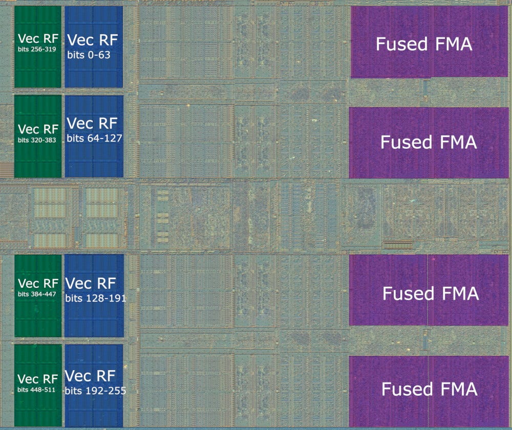
As described above, this second mode is also active when 256-bit and 512-bit operations are mixed. The vector unit can’t transition between 2×256-bit and 1×512-bit modes at fine granularity, giving the results we saw earlier.
Also thanks to Fritzchens Fritz, we can compare Palm Cove and Skylake (Coffee Lake)’s vector execution units. Here’s both die shots cropped to the vector execution section:
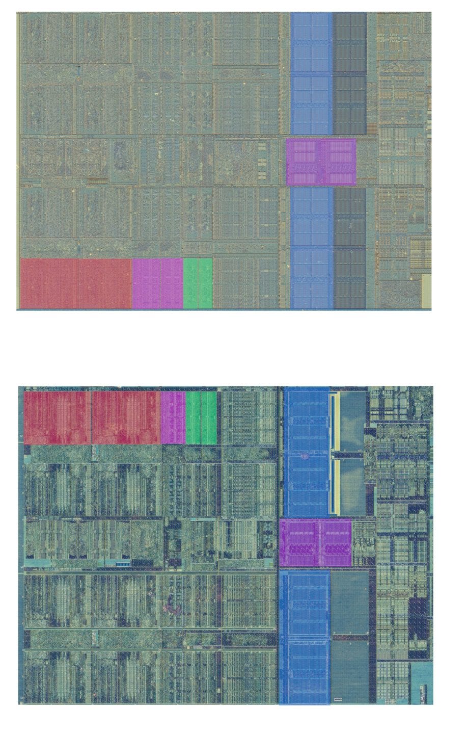
Palm Cove looks similar to Skylake’s, as we might expect. However, there are some extra execution units added to boost AVX-512 implementation. Let’s focus on one 64-bit section.
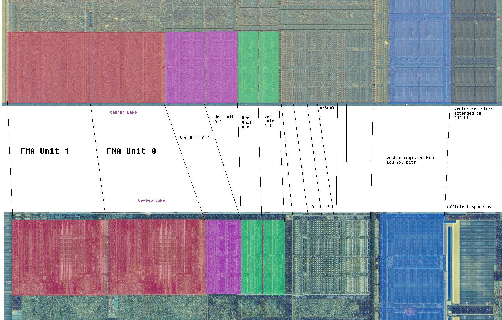
To the left, we can see the large FMA units, which were present since Haswell. Server Skylake duplicates these, but it’s easy to see why Intel opted not to do the same for Palm Cove. The FMA units simply take too much space. Adding more of them would be ridiculous on a client platform, where Intel has other goals for die area usage.
As we move from the left toward the register files on the right, we run a batch of mystery vector execution units. These are much harder to identify, but the unit immediately adjacent to the FP units seems to be extended. I wonder if that’s the vector integer ALU. We know that Palm Cove extends the integer ALU on port 5 to 512 bits. Closer to the register file, we see a mess of compute. However, from counting lines, there’s a bit of extra logic added right in the middle. Perhaps that has something to do with vector logic operations (no pun intended), which also have 512-bit execution throughput on port 5. If those guesses are correct, they demonstrate how cheap vector integer units are. It’s no surprise that Intel chose to implement more vector integer execution capacity, but avoided doing the same with floating point operations. On the far left, we can see that Palm Cove’s vector register file has been extended to 512 bits, just like in Skylake-X. This area was conspicuously unused in client Skylake.
If we look at where Palm Cove differs from Skylake, most of the changes come down to AVX-512:
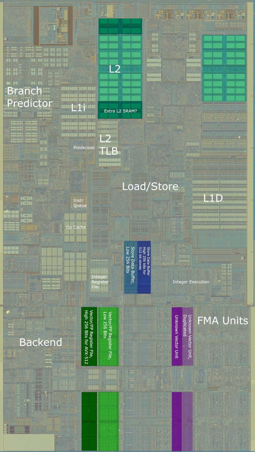
Besides the obvious changes to vector execution, we also see a structure between the load/store unit and integer datapath get extended. This is probably a buffer that holds pending store data, and its increased size suggests Palm Cove gets a boost to L1D performance. We can verify this with a bandwidth test.

AVX-512 lets the core handle 512 bits of data with a single address generation and L1D access, giving Palm Cove a large L1D bandwidth increase. Read performance is shown here, but the core can do a 512-bit store every cycle as well. Palm Cove apparently doesn’t throttle much if at all when faced with 512-bit memory operations. It therefore retains an actual bandwidth advantage against Kaby Lake. That’s no small feat, considering the i7-7700K clocks up to 4.5 GHz, which is more than 40% faster than the i3-8121U’s maximum 3.2 GHz clock.
Palm Cove also sees a small L2 bandwidth increase, pushing sustained throughput over 32 bytes per cycle. Client Skylake had a 64 byte per cycle datapath to L2 as well, but L2 bandwidth achievable with AVX instructions was limited by L1D bandwidth and interference from the L2 prefetcher.
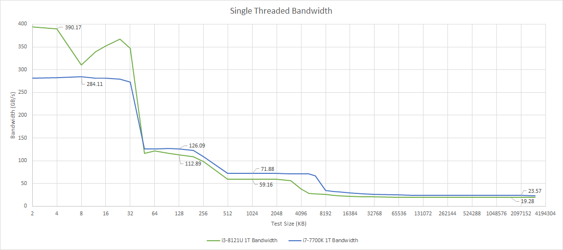
Multi-core bandwidth is impressive as well, for a dual core part. Kaby Lake does pull ahead here. That’s expected, because the i7-7700K has twice as many cores, running at much higher clocks.
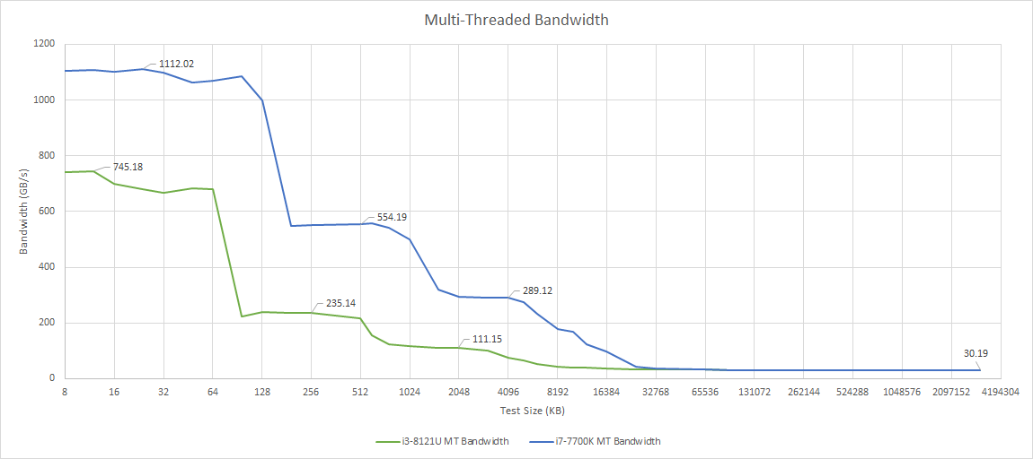
Palm Cove and Kaby Lake both achieve just above 30 GB/s of DRAM bandwidth in an all-thread read test. In fact, Palm Cove does slightly better, and hits 30.73 GB/s at the 4 GB test size. The i7-7700K lands a hair behind at 30.19 GB/s. Cannon Lake’s memory controller therefore is a hair more efficient, achieving 80% of theoretical bandwidth versus Kaby Lake’s 78.6% of theoretical. It’s not a big difference, and both memory controllers do a decent job with bandwidth.
Cache and Memory Latency
Palm Cove’s memory subsystem has very similar latency characteristics to Kaby Lake’s, in terms of cycle counts. However, the i3-8121U only has half as much L3. Intel scales L3 slice count alongside core count, so a dual core configuration only gets 4 MB, while the quad core i7-7700K gets 8 MB.
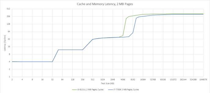
L3 latencies seem to differ by a just single cycle in Palm Cove’s favor, which is a bit surprising because Palm Cove should come out quite a bit ahead. To start, it’s using a smaller L3 cache on a shorter ring, which means fewer cycles are spent traversing the ring interconnect. Ring clocks can’t be an explanation either, because the i3-8121U runs the ring at 3.1 GHz, which is barely below its 3.2 GHz core clock. Compare that to the i7-7700K, which runs the ring at 4.1 GHz, while the cores run at 4.5 GHz. Most likely, Intel had to relax L3 timings during Palm Cove’s development. Maybe they were trying to aim for higher clock frequencies, but wound up being held back by other factors anyway.
If we look at actual latency, Palm Cove suffers due to low clock speeds. Kaby Lake is faster across the board.

DRAM latency is especially bad on Cannon Lake. Its LPDDR4 controller offered competitive bandwidth compared to the desktop DDR4 controller in Kaby Lake, but suffers from over 46% higher latency. The DDR4-2400 setup in Kaby Lake had reasonable 17-17-17-39 timings, while Cannon Lake’s LPDDR4 seems to have much higher timings. This will make it harder for Palm Cove to use the available bandwidth, especially if access patterns are not easily picked up by the L2 prefetcher.
Zooming Out
So far, we’ve focused on changes made create the Palm Cove architecture. Now, we’ll talk about Cannon Lake, the only product that Palm Cove was ever implemented in. Thanks to Fritzchens Fritz, we have a die shot showing what Intel was hoping to do with their 8th generation CPUs. That lets us speculate about stuff that we weren’t able to hit with software.
The iGPU: Glass Cannon Lake?
Cannon Lake’s iGPU is very large, and consumes 45% of the die all by itself. I’ve heard unsubstantiated rumors that the iGPU worked in Intel’s labs, but didn’t have a long enough average lifespan to make it into final products. In any case, we can’t test the iGPU from software because it’s disabled in the only Cannon Lake product that ever shipped.
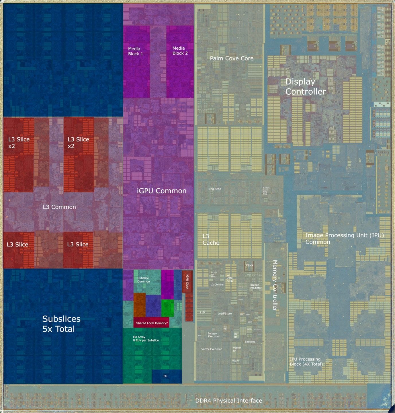
From the die shot, Cannon Lake received a much larger configuration than the GT2 setup we saw on most Skylake and Kaby Lake parts. We can see five subslices, each with eight EUs. For comparison, Kaby Lake and Skylake GT2 configurations also have eight EUs per subslice, but only three subslices.
Intel had been beefing up their integrated graphics with each generation, but the size increase with Cannon Lake is particularly large compared to previous generations.

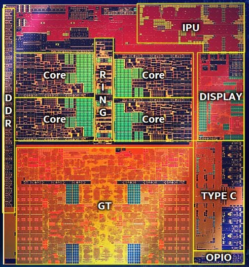
After Cannon Lake, Intel released Ice Lake in a quad core configuration, with a massive amount of iGPU compute power for a GT2 configuration. From the die shot, Intel really started accelerating their iGPU efforts in Cannon Lake.
To feed the EUs, Intel changed up their caching configuration. Intel’s iGPUs feature a confusingly named L3 cache, which functions as a last level cache for the iGPU. Memory accesses that miss the iGPU’s L3 then perform a lookup in the CPU’s L3, which is shared by the GPU. Cannon Lake moves the iGPU L3 into the center space between the subslices, putting it in a prime location to service requests coming from those subslices. That’s much better than in Gen 9.5.
While Gen 10 support has been removed from Intel’s Compute Runtime, old commits describe a CNL_2x5x8 configuration that closely corresponds to what we see in the Cannon Lake die shot. If that’s correct, Cannon Lake should have 1536 KB of L3 cache, arranged in six banks. For comparison, Gen 9 had 768 KB of L3, arranged in four banks.
Gen 10 also seems to change up the memory hierarchy by moving workgroup-local scratchpad memory (LDS in AMD terminology, shared memory for Nvidia, and SLM for Intel) from the iGPU’s L3 into each subslice. From the die shot, we see an unexplained large block of SRAM very close to the EUs. We don’t see an equivalent block on Gen 9.5.
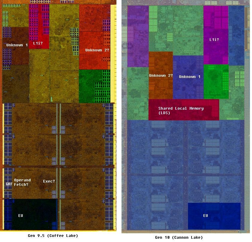
Moving local memory into the subslice creates a configuration that’s a lot more like what we see on Nvidia and AMD graphics architectures. Unlike a cache, local memory is explicitly managed by software, and is not visible outside a group of threads. In exchange for these limitations, software typically expects higher bandwidth and lower latency from local memory. Implementing local memory as part of the iGPU’s L3 probably made sense in very small configurations. But forcing local memory accesses to go through the subslice data port, which is also shared with global memory traffic, limits performance. Bringing local memory into the subslice should therefore improve latency and bandwidth, while reducing contention for subslice data port access. We know that Gen 11 did this, but there’s a strong possibility that Intel first experimented with this change on Gen 10.
Intel’s iGPU scale up efforts continue to fixed function hardware as well. Cannon Lake’s iGPU seems to have a very beefy media engine, with two large, replicated logic blocks. These might handle video encode and decode. We don’t see similarly replicated blocks in Gen9.5, suggesting that Cannon Lake would have had higher video processing throughput.
Cannon Lake’s Gen 10 thus looks like a large evolutionary step between the Gen 9 graphics architecture featured in Skylake based CPUs, and the Gen 11 architecture introduced with Ice Lake. From looking at the die shot and guessing though, Gen 10 looks a lot closer to Gen 11. Gen 10 seems to represent a sharp rise in Intel’s graphics ambitions, and part of a focus shift away from pure CPU power to more diverse on-chip capabilities. Intel’s engineers made a laundry list of improvements while also transitioning to 10 nm. But just as firing 20 pounds of shot out of a 2 pound cannon can have adverse effects on the structural integrity of the cannon, trying to do too much while moving to an extremely ambitious process node can adversely affect the final product.
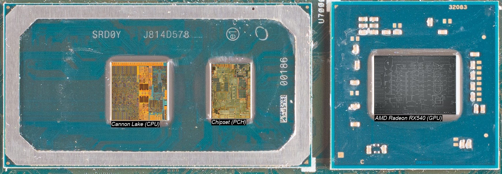
Cannon Lake was therefore forced to ship with a discrete GPU in order to drive the display. That’s a devastating setback for the nominally low power part, because a discrete GPU has to power up its separate pool of memory in order to function. The PCIe link between the CPU and GPU also has to be powered up. Because of this, laptops with discrete GPU typically still use the integrated GPU to drive the display, letting them power off the discrete GPU when heavy 3D rendering power isn’t needed. When the discrete GPU is active, it sends rendered frames to the iGPU, which displays them. Because Cannon Lake’s iGPU isn’t usable, it can’t use the same power saving technique.
Even though it never launched, the Gen 10 iGPU in Cannon Lake served as a proving ground where Intel’s engineers tried out significant changes. Features worked on for Cannon Lake’s iGPU finally saw the light of day when Ice Lake launched, and set a foundation for Intel’s future graphics adventures.
System Agent
At the cannon end of Cannon Lake’s iGPU, we have the display controller. Unlike the rest of the iGPU, the display controller sits in the system agent. From Sandy Bridge on, Intel’s client CPUs can be generally split into three parts: the cores and their cache, the iGPU, and the system agent. The system agent is responsible for handling IO functions, and generally fills the role of northbridge chips in older chipsets. Intel has always placed the display controller in the system agent, where it’s closer to both the memory controller, and the physical interfaces to the display connectors. The display controller can be a significant consumer of memory bandwidth, especially when the rest of the chip is mostly idle. Putting it in the system agent means the ring bus doesn’t have to be powered up to keep the display going.
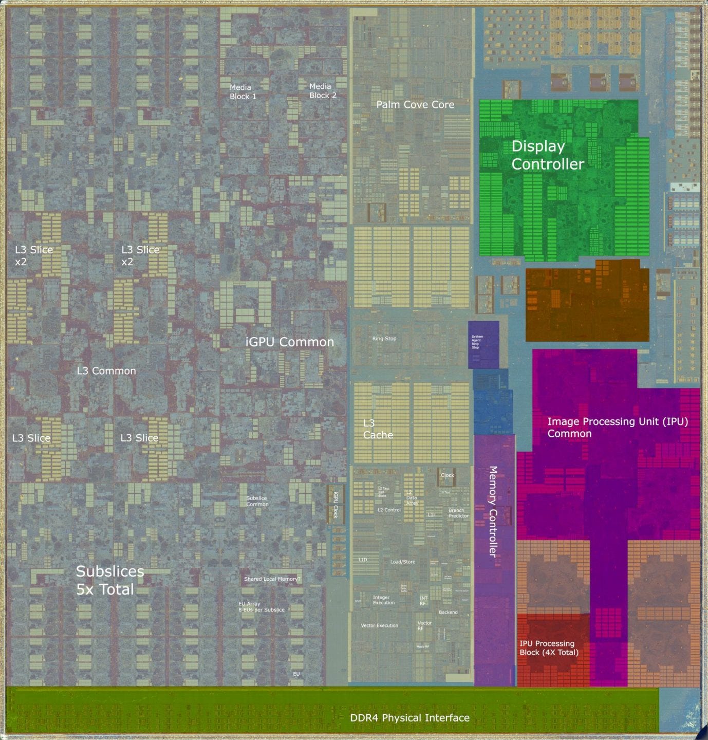
Compared to Skylake, Cannon Lake’s display controller has substantially more logic and SRAM. Intel states that the display controller uses its SRAM to buffer a large portion of the screen, and access memory in bursts. Assuming there’s not much traffic from the CPU or GPU, the memory controller can go into a low power state between bursts of accesses. When the chip is mostly idle but has to keep the display going, this strategy can help save power.
Another power saving strategy is to implement wider pixel pipes in the display engine, and run them at lower clocks. This costs more die area, but Intel stated that the tradeoff was worthwhile in their Gen 11 whitepaper. Going through Intel’s graphics documentation, we can see Intel’s display controller evolve every generation to handle higher resolutions while improving power efficiency.

Cannon Lake’s display controller should fall between Skylake’s and Ice Lake’s, though it’s probably closer to the latter. We’ll never know if Cannon Lake could drive 8K displays like Ice Lake, but the large increase in SRAM blocks does suggest Intel was aiming higher than 4K.
Cannon Lake’s system agent is also home to a very large Image Processing Unit (IPU). Raw camera sensor data requires significant processing to generate a frame for display. For example, individual pixels on a camera sensor only provide the intensity of detected light at that point1. Each pixel has a filter over it that only lets a certain color through. Full RGB values are reconstructed for each pixel by looking at values from surrounding pixels with different color filters over them. The IPU can handle this color reconstruction process, among many other tasks.
Of course, this can be done on a CPU core as well. But as laptop webcams get higher resolutions, offloading these computations to dedicated hardware could provide higher power efficiency. That’s especially important for tasks like video calls on a battery powered device. Because the IPU writes processed frames out to memory, it sits next to the memory controller in the system agent. Compared to the IPU in Kaby Lake and Skylake, Cannon Lake’s IPU is very different and has a layout comparable to the one in Ice Lake.
In addition to the IPU, Cannon Lake features a first generation Gaussian and Neural Accelerator (GNA). While the IPU offloads camera frame processing, the GNA is meant to offload machine learning based noise cancellation and speech processing. We don’t know much about the GNA, but Intel’s slides suggest that it has a memory scratchpad as well as a wide SIMD math unit. I doubt the GNA has a significant amount of throughput. On the die shot, it’s probably located between the IPU and display controller, and would be smaller than both. Intel’s slides say GNA saves about 50% of a 1.1 GHz Atom core, which also also suggests the design prioritizes power saving over raw compute power. To do this, GNA probably runs a very wide SIMD unit at low clocks, and saves on data transfer power by pulling data from nearby SRAM. Together with the IPU, the GNA would help lower power consumption in videoconferencing applications.
Conclusion
Cannon Lake is a story of Intel’s dreams for the future, in an era where it had an unchallenged CPU performance lead. CPU development has a very long lead time, so Cannon Lake’s goals were probably set well before AMD’s Zen launch. After Haswell and Skylake, Intel already controlled almost all of the desktop and laptop CPU market. Bringing more CPU power wouldn’t really change that. AMD had given up on high end desktop ambitions after Piledriver. In the laptop and budget market, AMD’s dual module, quad thread designs didn’t really compete with Intel’s dual core CPUs in terms of CPU performance and power efficiency. Instead, AMD tried to use their graphics IP to stay in the game.
Intel therefore wanted to stamp out the last remaining AMD competition by allocating die area to supporting hardware, instead of using it to boost CPU performance. Of course, the cores still saw some changes. Palm Cove does get AVX-512 support, and a few changes here and there. But I would classify the latter as tweaks on the Skylake architecture rather than new substantial features. AVX-512 is important, but the foundations for AVX-512 were already laid in client Skylake. Palm Cove just had to fill in the blanks, shrink a few things from server Skylake and its AVX-512 implementation was ready to go.
Outside the cores, Cannon Lake has a scaled up and improved iGPU implementation. More cache within the iGPU helps performance scale further without memory bandwidth limitations. AMD’s Kaveri and Bristol Ridge APUs had more FP32 lanes (8 CUs, or 512 FP32 lanes versus 320 on CNL), but Intel’s iGPUs typically run at over 1 GHz. Bristol Ridge only clocked its iGPU up to 900 MHz, which means AMD’s lead in FP32 throughput isn’t as large as “shader count” might suggest. Intel also implemented a large IPU and GNA within the system agent. Like cell phone SoCs, Cannon Lake was trying to improve battery life by offloading processing to more efficient fixed function hardware. AMD had no answer for these fixed function blocks, and would likely be at a disadvantage against a fully enabled Cannon Lake part. Intel’s advantage would be especially clear in applications like videoconferencing, where audio processing could be offloaded to the GNA, and video processing could be handled by the IPU. Optimizations in Cannon Lake’s display controller would further improve power efficiency.
In a different timeline where AMD failed to become competitive again, we would all be using Intel laptops. CPU performance gains would be minor, but they would have increasingly powerful integrated GPUs and other supporting hardware. These laptops would have long battery life especially for applications like videoconferencing and video playback. Intel would keep going along this route, hoping to compete with ARM based products in the tablet space. And Intel’s U-series mobile chips might start looking a lot more like cell phone SoCs, where a lot of die area is spent on implementing hardware acceleration blocks, and the CPU takes a back seat.
But none of this became reality. The iGPU never launched in a working product, forcing Cannon Lake to drive the display with a discrete GPU and devastating its power efficiency. 10 nm process issues likely forced the CPU to run at a low clock speed, meaning that it failed to compete with prior generations of Intel CPUs. Intel’s fantasies were sort of realized when Ice Lake got a limited release on mobile platforms, with working integrated graphics. But by then, AMD’s return to competitiveness with Zen was in full swing. Intel quickly turned around and allocated die area toward improving multithreaded CPU performance. Today, AMD and Intel are neck and neck in both the mobile and desktop market, with both vendors pushing CPU performance as hard as they can.
If you like our articles and journalism and you want to support us in our endeavors then consider heading over to our Patreon or our PayPal if you want to toss a few bucks our way or if you would like to talk with the Chips and Cheese staff and the people behind the scenes then consider joining our Discord.
Footnotes
(1) Yes, I know there are camera sensors out there that can detect all three colors with one pixel. Sigma’s Foveon sensors are one example, but Bayer-patterned sensors are by far the most common, and I don’t think laptop webcams will be using exotic sensor technology anytime soon.
Credits
Huge thanks to cha0s for running the tests on Cannon Lake and donating the chip for a die shot. And thanks to Fritzchens Fritz for taking the best die shots around, for free.
Hey, great read as always, it’s wild how that single Cannon Lake SKU truely foreshadowed Intel’s protracted 10nm struggles, right?