
Microbenchmarking Intel’s Arc A770


Intel’s Arc GPUs represent the company’s third attempt at taking on the dedicated GPU market. The company’s first attempt, the i740, tried to use the then-new AGP interface to store textures in system memory. In theory, the i740 could get by with less onboard memory and simplify programming by removing the need to copy textures into VRAM. That failed badly, and Intel learned that a high performance discrete card can’t heavily rely on the host connection. Larrabee was their second attempt. It integrated a ton of in-order CPU cores with wide vector units, but lacked a lot of the fixed function hardware found in GPUs. Larrabee never launched, and Intel learned that a CPU is not a GPU.
With these valuable lessons in mind, Intel is using their Xe-HPG architecture to take another shot at creating a high performance GPU. Xe-HPG traces its ancestry back to a long line of Intel integrated graphics architectures. It’s closely related to the Xe-LP graphics architecture used in Intel’s current integrated GPUs, but adds hardware accelerated raytracing, matrix units. More crucially, it’s designed to scale to much larger configurations.

The Arc A770 features 512 EUs, for a total of 4096 FP32 lanes. That’s several times larger than any integrated GPU from Intel, and shows a clear intention to take on the midrange discrete GPU market. Here, we’re going to run various microbenchmarks on A770. Hopefully that’ll give insight into how Intel’s architecture compares to Nvidia and AMD’s, as well as how Intel has evolved their graphics architecture to work in larger configurations.
Terminology
In the GPU world, everyone uses different terms to describe similar things, resulting in endless confusion. Just to get everyone on the same page:

Memory Hierarchy
A big part of scaling up a GPU is making sure the memory hierarchy can feed of all the execution units. We’ll start by testing memory latency to give us a good idea of the cache setup.

Intel and Nvidia employ a traditional, two-level cache hierarchy like most GPUs we’ve seen over the past decade. Intel’s strategy here is to employ larger caches than the competition. At L1, the Arc A770 trades some latency to provide a L1 that’s at least 192 KB in size. In contrast, each Nvidia Ampere SM has a 128 KB block used for both local memory and L1D, and seems to have allocated 96 KB as L1D in our OpenCL testing. While lower L1D latency is obviously better, a GPU at high occupancy should have no trouble hiding that sort of latency. Higher L1 hitrate should also improve average access latency, because fewer requests have to be serviced by L2 and beyond.
Intel’s L2 is large as well. At 16 MB, it’s several times larger than the L2 caches found on AMD and Nvidia cards. Despite the L2’s large size, Intel was able to maintain relatively good latency characteristics. Arc A770 can get data from its L2 slightly faster than the RTX 3060 Ti can, even though the Nvidia card only has a 2 MB L2. AMD’s L2 has lower latency, but is also smaller.
In contrast to Intel and Nvidia, AMD’s RDNA 2 uses a complex four-level cache setup and trades blows with Arc depending on the test size. I find it especially interesting that Intel’s L2 is bracketed by AMD’s L2 and Infinity Cache both in terms of capacity and latency.

VRAM access latency is higher on Arc than on contemporary AMD and Nvidia cards, and reminds us of some older products from around a decade ago. Memory latency isn’t as huge of a factor for GPUs as it is on CPUs, because GPUs rely on very high occupancy (high thread counts) to hide memory latency. You can imagine how SMT makes a CPU core less sensitive to memory latency, because the core has a higher chance of finding independent work to do while waiting for data to arrive from memory. GPUs work in the same way, but take it much farther. For example, an Xe-HPG “Vector Engine” can keep eight threads in flight, basically giving it 8-way SMT. Then, an Xe Core has 16 vector engines. AMD and Nvidia GPUs work similarly, but have differently sized subdivisions.
Bandwidth
To illustrate the point with occupancy, let’s look at memory bandwidth from a single workgroup. This is as close as we can get to GPU single core bandwidth. By dispatching a single workgroup, we can force the GPU to execute all of our OpenCL kernel invocations on a single unit of compute with its own local memory. That is, a single Arc Xe Core, Nvidia SM, AMD RDNA WGP, or AMD GCN CU. With one workgroup, Arc can achieve the compute throughput of a Xe Core rather than an 8-wide Vector Engine, so we’re pretty sure our single workgroup test is running on an Xe Core.

One Arc Xe Core can’t pull a a lot of bandwidth across the memory hierarchy. VRAM bandwidth is especially poor. An AMD 6600 XT WGP or Nvidia RTX 3060 Ti SM can get 63 or 34.4 GB/s from VRAM, respectively. A Xe Core’s 8 GB/s makes it look like an old CPU core in comparison. Latency is definitely a culprit here, but there’s more to the story. A single CU from AMD’s old HD 7950 can also pull several times more bandwidth from VRAM, even though it has similar VRAM latency. Cache bandwidth isn’t great either, suggesting that Arc’s Xe Core has limited memory level parallelism capabilities compared to other GPUs.
Most GPUs can handle workgroups with 256 threads, so we’re using that as our default test size. Each kernel invocation in this test uses float4 vectors, this test has an explicit parallelism factor of 256 * 4 = 1024 FP32 items. Arc supports workgroup sizes up to 512 threads, so we did additional testing on the A770 with workgroup size maxed out. If you see “Local Size=512” that means that for that test we are using 512 threads. This also means that for any Local Size=512 test, Arc’s Xe Core has twice as many threads in flight to switch between and use to hide latency. For a sense of scale, a single thread using AVX-512 would expose an explicit parallelism factor of 16 FP32 items, and two such threads running on the same core via SMT would bring parallelism factor to 32 FP32 items.
With double the explicit parallelism, an Xe Core sees improvement and almost catches Nvidia’s Ampere in terms of L2 bandwidth. However, VRAM bandwidth is still disappointing, with AMD’s old GCN architecture still pulling ahead. In fact, the A770’s single workgroup bandwidth is closest to the very old AMD HD 5850. That card is based on the Terascale 2 architecture, and can give a single workgroup 18 GB/s from VRAM with half as much parallelism available.
Shared Cache Bandwidth Scaling
As you can tell, testing GPUs is tough. But we’re starting to see signs that Arc doesn’t do well with a limited amount of work in flight. Of course, applications are supposed to use more than one GPU core at a time. Let’s increase the workgroup count, and see what happens with cache bandwidth as more Xe Cores, SMs, and WGPs get loaded. Shared caches are difficult to implement because they have to serve the bandwidth needs of a lot of consumers, and bandwidth demands on GPUs can be especially high. Ideally, we should see bandwidth scale as high as possible. But we also want it to hit high bandwidth with as little parallelism as possible, because that means the bandwidth will be easier to utilize.

Intel’s Arc A770 doesn’t scale anywhere near as well as its competitors. Nvidia and AMD both achieve higher bandwidth at a given level of parallelism. Incredibly, AMD’s Infinity Cache scales better than A770’s L2. That’s a pretty poor showing for Intel’s cache implementation, because Infinity Cache has higher capacity and a higher bandwidth L2 sitting in front of it. Arc clearly needs a lot of work in flight to take advantage of its bandwidth potential. We would have run this test with even more workgroups to see just how much parallelism Arc needs to catch up, but the A770 runs into some issues with our test suite.
These issues are also why the Local Size=512 test ends at 19 workgroups despite showing better results. Intel’s drivers seem to have issues when a program repeatedly allocates and frees memory on the card. After 19 workgroups, corresponding to 19 runs of the bandwidth test, Intel’s OpenCL runtime reports that it can’t allocate more memory because it’s out of resources. We don’t see issues on other cards even with more repeated runs and older drivers. For example, the Vega VII happily went up to 60 workgroups, or 60 repetitions of the bandwidth test with different workgroup counts, and didn’t encounter issues.
If we test VRAM sized regions, Arc has similar difficulty scaling. AMD and Nvidia both saturate their VRAM bandwidth pretty quickly and don’t need all of their WGPs or SMs in play to do so. Nvidia does need a few more SMs loaded to make good use of its memory bandwidth, but that’s largely because Ampere has a lot more memory bandwidth on tap. With similar levels of parallelism, Nvidia isn’t far off where AMD is. Intel however is on a different planet. The A770 cannot saturate its VRAM bandwidth even with all 32 of its Xe Cores active. Clearly, we need more work in flight for Intel’s GPU.

So, let’s test bandwidth with 512 workgroups. That should be enough to fill out all of the compute units across a GPU, with plenty of work for each. On the A770, that means each Xe Core should have 16 workgroups, each with 256 threads, each dealing with float4 vectors, giving an explicit parallelism factor of 16384.

At high occupancy, Intel’s Arc A770 finally shines, with competitive bandwidth throughout its memory hierarchy. Intel has done a good job of making sure their shared L2 cache and memory controllers can scale to feed large GPU configurations. However, Intel’s architecture will require high occupancy workloads to really shine, and high occupancy is not a guarantee. For example, take this frame rendered from GHPC, a game that lets you do things to simulated T-72s. Pay attention to the large number of small “Dispatch” calls followed by barriers around 17-18 ms
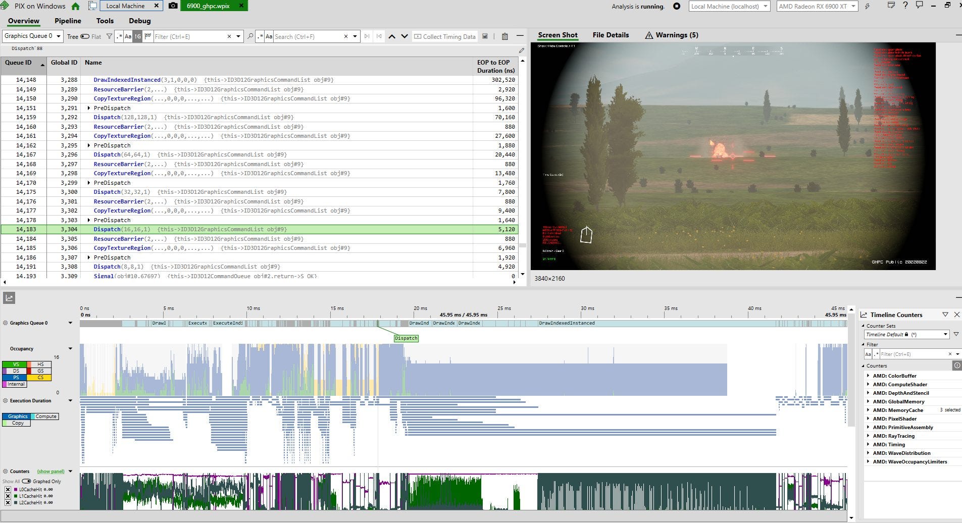
Such a sequence of commands would be difficult on any GPU, but Arc will have a much harder time coping than a contemporary AMD or Nvidia GPU, or even one from a years ago. Other examples of low occupancy workloads include vertex shaders. Of course, high occupancy loads are important too. Examples include pixel shaders, especially at high resolutions. Arc has a good chance of scaling better at high resolutions, where it can take advantage of a ton of explicit parallelism to catch up. Arc’s disadvantage with small work sizes can also be mitigated by async compute.
Local Memory Latency
On GPUs, local memory is a small block of scratchpad memory, shared by all threads in a workgroup and not accessible outside the workgroup. Software has to explicitly load data into local memory, and local memory contents are gone once a workgroup finishes execution. That makes local memory more difficult to use, but in exchange, local memory typically offers faster and more consistent performance than the normal global memory subsystem. One use of local memory is to store a BVH traversal stack when raytracing.

Intel’s Arc A770 enjoys decent local memory latency, though it is slightly behind current cards from AMD and Nvidia. It’s similar to Nvidia’s Maxwell based GTX 980 Ti in this regard, which isn’t impressive, but isn’t bad either. More importantly, Intel has been making steady progress in this area. Older generations of Intel iGPUs implemented local memory as part of the iGPU’s L3 cache (not to be confused with the CPU’s shared L3), resulting in high latency. Starting with Gen11, implemented in Ice Lake’s iGPUs, Intel moved local memory into the subslice, dramatically improving latency. A770 further improves on that, which is great to see.
PCIe Link Bandwidth
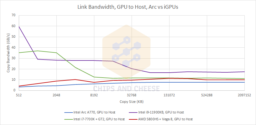
Discrete GPUs differ dramatically from their iGPU counterparts in how they’re connected to the host. With integrated GPUs, Intel enjoyed very high bandwidth between GPU and host CPU. They could even avoid copying data without performance penalty, because the integrated GPU and CPU share the same pool of memory. But discrete GPU trade off this high speed communication in favor of a getting their own pool of very high bandwidth VRAM.
Unfortunately, we weren’t able to get the A770 set up with PCIe 4.0. However, resizeable BAR was enabled. And that lets us illustrate the difference Intel has to deal with coming from their iGPU background.
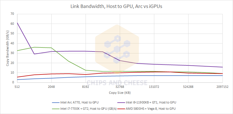
Intel tightly integrates their iGPUs by putting them on the same ring bus that serves the CPU cores, letting the iGPU share the CPU’s L3 cache. Small copies from the CPU to GPU can be backed by the L3 cache, providing insanely high copy bandwidth. The same applies in the other direction.
AMD doesn’t have a shared cache between the iGPU and CPU, but still enjoys an advantage because the shared DDR4 memory bus has more bandwidth than PCIe.
If we compare the A770 against the AMD’s 6600 XT and 6700 XT, or Nvidia’s 3060 Ti and 3070 as we did earlier, Intel obviously gets left behind because of the PCIe 3.0 configuration. AMD has a particularly large advantage when copying data to the GPU, because the resizeable BAR feature allows mapping all of the GPU’s VRAM directly into the CPU’s physical address space.

AMD’s implementation is less optimized for copying data from GPU back to system memory. Nvidia and Intel don’t see as much of a drop when transferring data in the GPU to host direction. With PCIe 3.0, Intel’s A770 is most comparable to Nvidia’s GTX 980 Ti. The Maxwell based 980 Ti does slightly better wtih small copy sizes, while Intel pulls off a slight lead with larger copies.

All in all, there’s nothing wrong with A770’s PCIe link as far as our limited testing can see. It performs about as expected when operating at PCIe 3.0 speeds, though it’s disappointing to see that the A770 did not pull a PCIe bandwidth lead over the GTX 980 Ti, which lacks resizeable BAR support. Keep in mind transfer speeds will often not approach theoretical limits because of protocol and API overhead.
We also ran our test on GPUs with different PCIe generations, without resizeable BAR. As expected, the Arc A770 on the PCIe 3.0 equipped i9-9900K platform clearly outperforms a PCIe 2.0 one. In this case, that’s the AMD HD 5850, connected to a FX-8150 CPU.
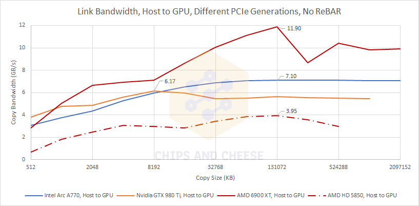
However, the difference isn’t as large as you might expected. There’s probably a lot of overhead associated with moving data between the CPU and GPU’s memory pools. For example, if the HD 5850 is able to pull about 5 GB/s over the PCIe bus when it runs out of VRAM and has to use host memory as swap.

Surprisingly, Terascale does better when pulling data off the GPU to the host, while more modern cards tend to do slightly worse. In any case, Intel’s A770 has a nice link bandwidth advantage compared to AMD’s card from 2009.
Compute
Arc’s launch comes at an inconvenient time because our GPU microbenchmark suite is still very much a work in progress. We have a relatively new test for instruction execution rates and latencies, but unfortunately it’s not working very well on the A770. For example, we got 11.4 TFLOPS of FP32 FMA throughput on the AMD 6700 XT and 21.6 TFLOPS on the Nvidia RTX 3070, but only 4.75 TFLOPS on the Intel A770. We get better results when using a single workgroup to target one Xe Core/SM/WGP. Therefore, we’ll focus on per-clock, per-GPU building block measurements. Also, we see some higher than expected variation especially when testing on Nvidia Ampere, so do take these results with a grain of salt.
Arc’s Xe Core has similar FP32 throughput to the basic building blocks in RDNA 2 and Ampere. We’ll also draw comparisons to a few other architectures, as listed below. Because different GPUs have differently sized building blocks, we’re mostly looking at how close we get to theoretical throughput. The closer, the better.
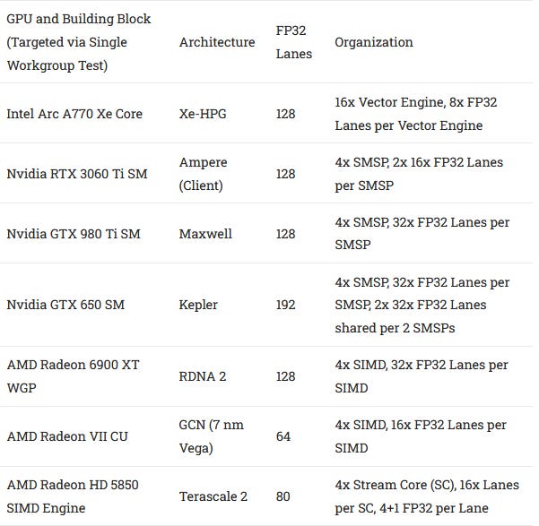
FP32 throughput is one of the headline features of any GPU, and graphics rendering tends to involve a lot of FP32 operations. Compared to other GPUs with 128 FP32 lanes per basic compute unit, Arc’s Xe Core is reasonably competitive when doing FP32 addition. Intel also achieves a good percentage of its available throughput. However, it struggles with fused multiply add, which is also a very common operation.

This test uses OpenCL code to compute a += a * b, which should avoid any register file bandwidth issues because one input can be used twice. We also tried with OpenCL’s mad function in case Intel’s driver was unwilling to convert the test expression into a fused multiply add instruction, but that made no difference. Intel’s Xe Core is behind even Terascale 2 if we look at percentage of theoretical throughput achieved in this test. Why it ends up there is a mystery.
GPUs also have to deal with integer operations from time to time, though there are typically far fewer integer instructions than floating point ones. Arc has reasonably good integer addition throughput.

However, Arc is quite a bit off from other recent architectures, which can use all of their FP32 to handle INT32 as well. Nvidia actually achieves slightly more integer throughput than they should theoretically have. I count incrementing the loop iteration counter as a 32-bit integer operation, and suspect Nvidia is dual issuing that instruction on Maxwell. On Ampere, maybe that’s handled via the uniform datapath introduced in Turing. Nvidia might have another way to handle loop operations without performing a calculation on each vector lane.
INT32 multiplication throughput is much lower than addition throughput on all recent architectures. Nvidia’s Ampere is an exception, and can handle integer multiplication at half rate.
FP64 was not tested because the Arc A770 doesn’t support it.
Execution Latency
GPUs don’t come to mind as low latency devices, and that applies to execution latency as well. Unlike CPUs, they rely on high occupancy to hide execution latency, but latency can still be a factor in GPU performance, so we’re going to take a surface level look at it.

Surprisingly though, modern GPUs have very decent floating point execution latencies. AMD and Nvidia’s current GPUs are actually CPU-like in this area. For comparison, FMA latencies on AMD and Intel’s current CPUs are 5 and 4 cycles respectively. Of course, those CPUs clock higher, but the clock speed gap isn’t gigantic compared to low power mobile and server CPUs..
Arc’s latencies are generally higher. Its FP32 addition latency is acceptable, landing just under Kepler’s. But FMA latency is worse than other GPUs we’ve looked at. Maybe Arc was latency bound in the execution throughput test above, but I doubt that’s the case because 11-12 cycles is not high at all in the absolute sense. A GPU scheduler with several threads to pick from, and many independent FMA operations per thread should have no trouble hiding that level of latency. AMD’s Terascale 2 architecture also suffers from relatively high FP32 latency, and still makes better use of its theoretical compute capacity in our throughput test.

GPU integer execution latency is generally similar to FP32 latency, and is sometimes a bit lower. Arc does better in this area than Kepler and Maxwell, but again lands a bit behind newer AMD and Nvidia GPUs. Integer multiplication seems to be a special case where all GPUs struggle. Nvidia has put a lot of emphasis on INT32 execution starting with Turing, and has the best multiplication latency. The A770 and GTX 980 Ti both struggle with integer multiplication, though I can’t recall seeing any integer multiplies in disassembled game and compute code. So I think INT32 multiply is a rare operation that doesn’t see much optimization on GPUs.
It’s hard to quantify how Arc’s higher execution latency might affect performance, but metrics gathered via Nvidia’s Nsight profiler should offer some perspective. To handle execution dependencies, Nvidia uses software assisted scheduling. Control codes embedded alongside instructions tell the warp scheduler how long it should wait before results from previous instructions are ready, and execution can continue. The “wait” warp stall reason therefore corresponds to stalls due to execution latency.

We can see that execution latency stalls are minor compared to “long scoreboard” (global memory latency), but they’re still a significant part of execution stalls unrelated to the slow global memory subsystem. We can also see the impact of Ampere’s reduced execution latency compared to Pascal. 5.29% of warp stalls on the GTX 1080 were attributed to execution latency, but that figure drops to 3.56% on the RTX 3090. Arc’s execution latency for common operations is higher than both of those architectures, so Arc will need higher occupancy to hide execution latency effectively.
Raja versus Raja
Many people have been making jokes that Arc is just Vega but with Intel branding stuck on to the side. So we decided to test one of the Radeon VII’s that one of our editors has to see just how close to these jokes are to reality.

In terms of memory latency, Raja has a lot to be proud of. Arc has larger caches at both levels, with equal or better latency. VRAM latency sees a regression, but the larger L2 should ensure Arc doesn’t have to hit memory as often as Radeon VII does. Now, let’s look at bandwidth.

For a single workgroup, at 256 threads per workgroup the Radeon VII beats the A770 at all test sizes. We need to go to 512 threads per workgroup for the A770 to beat the Radeon VII prior to going out to VRAM sized regions. At VRAM sized regions, the Radeon VII has the bandwidth win over the A770 regardless of the number of threads that the A770 is using. The A770 needing double the number of FP32 items of the Radeon VII to get better bandwidth is not good considering that the Radeon VII already had occupancy issues.

Looking at the scaling for more CUs/Xe Cores at the L2 level, for 256 threads we see that again the Radeon VII is scaling much better then the A770. With 512 threads, A770 gets much closer to the Radeon VII but A770 needs twice as much parallel work to achieve this result which points to the A770 having even more reliance on high occupancy than the Radeon VII.

At VRAM regions, the Radeon VII’s bandwidth scaling isn’t great compared to more modern cards, but it still convincingly outperforms the Arc A770. At high occupancy, the Radeon VII has a massive bandwidth advantage, thanks to its HBM memory setup. Intel does have a larger L2 cache and should be less reliant on memory bandwidth. Unfortunately, Arc’s L2 bandwidth actually falls behind the Radeon VII’s memory bandwidth at low occupancy.
At high occupancy, Arc shows off a large cache bandwidth advantage, just as it did against its modern competitors. Again, the A770’s L2 provides an impressive amount of bandwidth considering its size. The Radeon VII on the other hand uses a smaller L2, and a much higher bandwidth HBM memory setup.

Compared to contemporary cards, the Radeon VII had a lot of compute power and a lot of bandwidth on tap, but required more explicit parallelism to take advantage of it. Intel’s Arc A770 similarly bests its competitors in theoretical compute throughput and needs high occupancy to do well. However, the A770 trades the expensive HBM memory setup for a more modest 256-bit GDDR6 one, and uses a much larger L2 to avoid memory bandwidth bottlenecks.
For everyone that calls Xe-HPG “Vega 30”, there is some truth in that statement. While the building blocks for the Radeon VII and Xe-HPG are very different, the reliance on high occupancy is something that both architectures rely on. If anything, Xe-HPG is even more reliant on high occupancy than Vega is. This partly explains why the A770 scales so well to higher resolutions because higher resolutions will keep the GPU at higher occupancy levels. We saw this behavior with Vega except it is even more prevalent here with the A770.
Thoughts on Intel’s GPU Building Blocks
In the terminology section, we noted how Intel’s Xe core is similar to Nvidia’s Streaming Multiprocessor (SM) or AMD’s Workgroup Processor (SM). All three have their own local memory and instruction cache, and function as a basic GPU building block. Nvidia’s SMs and AMD’s WGPs are superficially similar. Both are divided into four partitions. Each partition has a scheduler block and a register file to feed 32 FP32 lanes. Intel’s Xe Cores also have a total of 128 FP32 lanes, but divide them into 16 partitions, called Vector Engines.
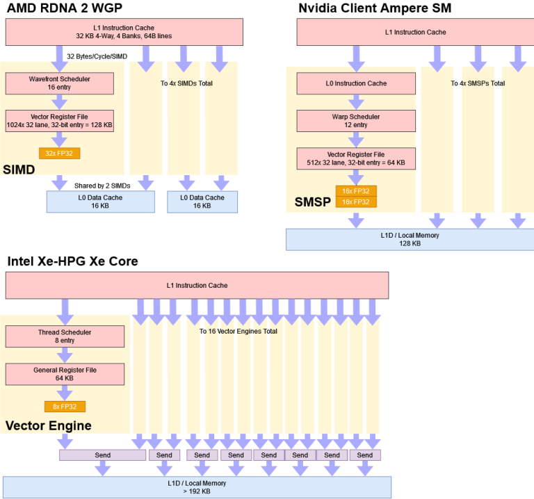
Vector Engines trace their ancestry to the Execution Units (EUs), which were the basic building in Intel’s integrated graphics. Starting from Ivy Bridge, these EUs were 8-wide, and let Intel scale iGPU configurations in very small increments, which was important when Intel was building very small iGPUs. For example, an Ivy Bridge GT1 configuration had six EUs (48 FP32 lanes) in a single subslice, and was paired with lower power dual core CPUs. The GT2 configuration used on quad core desktop CPUs had 16 EUs (128 FP32 lanes), with eight per subslice. Contrast that with AMD’s GCN architecture, which could only scale in increments of 64 FP32 lanes.
With Xe-HPG, Intel renamed the subslice to “Xe Core”, put eight pairs of EU/Vector Engines in it, and made that the basic building block. Each pair of vector engines share a “Send” port, which is used to access the memory subsystem. Each Xe Core’s L1 cache therefore has to arbitrate between requests from eight “Send” ports. Each of those “Send” ports is arbitrating between requests from two Vector Engines. Contrast that with Nvidia SM, where the L1 only has to handle requests from four SMSPs, or AMD’s CU, where the L1 only has to handle requests form two SIMDs. Intel’s Xe Core has a very complex load/store system because of the small subdivisions within it, and complex things are harder to do well.

Intel’s OneAPI Optimization Guide suggests that the load/store system services the EUs/Vector Engines in a round robin fashion, which means that each of the eight memory bandwidth consumers would be serviced every eighth cycle. I wonder what happens if the vector engines unevenly demand bandwidth. Hopefully, the Xe Core only cycles between active requestors. But if it doesn’t, that could explain a lot of the bandwidth issues we see at low occupancy.
Final Words
Intel has done a lot of work to move their graphics architectures into higher performance segments. As far back as Haswell, Intel experimented with scaling up their integrated graphics configurations, and used large EDRAM caches to avoid running into memory bandwidth bottlenecks. They continued this effort for years, tweaking the architecture and scaling it up in subsequent generations. Intel was targeting very low end discrete GPUs with these early efforts, but their engineers were slowly getting experience in scaling out the architecture and hitting higher performance targets. Sooner or later, they would aim to create credible discrete GPUs, capable of taking on something more than very low end AMD and Nvidia cards.
These efforts culminated in the Arc series discrete GPUs we see today. To create the A770, Intel scaled up their Xe Core counts to provide competitive compute throughput against AMD and Nvidia’s midrange cards. They also scaled up the cache and VRAM subsystem to feed those cores. In terms of cache and memory bandwidth, A770 can match or beat its competition. I’m impressed with Intel’s performance in that respect, because the company didn’t have much experience with large GPUs.
However, A770 ended up hitting a bit lower than what Intel probably intended. We didn’t do gaming benchmarks ourselves because there’s already a ton of people doing that online. From results across the internet, the A770 seems to compete more with the RX 6600 XT than the 6700XT. On paper though, the A770 should have no trouble standing head and shoulders above the 6700XT. I suspect that’s because the A770 needs a lot of work in flight to really shine. Intel probably does well when handling operations executed across every pixel in a high resolution frame. It probably doesn’t do as well when when pixel or other high occupancy work is a smaller fraction of the work needed to render a frame.
From an architecture standpoint, the Arc A770 still has elements that are better suited to use in small integrated graphics implementations. But these elements are slowly going away as well. Xe-HPG’s Vector engines are arranged in pairs that share scheduling logic and a data port. Intel’s HPC architecture variant, Xe-HPC makes vector engines twice as wide and uses half as many per Xe Core. Perhaps Intel will continue in this direction going forward.
Hopefully, Intel will make other changes as well to make their future graphics architectures more capable with low occupancy workloads. Today, the A770 is a mixed bag that shows strengths in cache bandwidth and potential compute throughput, but struggles when parallelism is limited. Xe-HPG does in some ways feels like a spiritual continuation of GCN, a GCN 6.0 if you will. If Intel can fix these problems and have a “RDNA moment” with later GPU architectures, they could have a very solid product that can take on Nvidia and AMD’s GPUs head on for the performance crown. And I really do hope that Intel can make that happen, because more competition is always good for everyone.
If you like our articles and journalism and you want to support us in our endeavors then consider heading over to our Patreon or our PayPal if you want to toss a few bucks our way or if you would like to talk with the Chips and Cheese staff and the people behind the scenes then consider joining our Discord.
Credits
This article would not have been possible without the many volunteers who tested their cards and provided data. We’re a batch of enthusiasts who don’t have large collections of GPUs and CPUs like other review sites. Without help from our awesome community, I might be comparing the A770 to the HD 5850 and calling it a day. That’s a joke – of course I’d include Kepler as well. Anyway, special thanks to:
Dayman, for testing the A770
Cha0s, for testing the GT1 integrated GPU on Tiger Lake
Eraser, for testing the Nvidia RTX 3070
Serebit, for testing the AMD Radeon 6600 XT
Smcelrea, for testing the Nvidia RTX 3060 Ti and AMD Radeon 6700 XT
Sask, for testing the AMD Radeon VII
Updates
10-20-2022: Updated the article to indicate that resizeable BAR was enabled on the A770. Added credits too.