
Hot Chips 34 – Biren’s BR100: A Machine Learning GPU from China

Previously, we covered Tesla’s Dojo, an unconventional CPU architecture specifically designed for neural network training. We also looked at AMD’s CDNA2, a GPU architecture focused on high performance compute. Now, we’re going to look at Biren’s BR100, a GPGPU that strongly focuses on machine learning. It’s CDNA2’s opposite in some ways. Unlike AMD’s HPC focused architecture, BR100 has no FP64 support. Instead, it has matrix units that give it massive throughput with lower precision formats like BF16.
BR100 is interesting because it’s structured very differently from AMD and Nvidia’s GPUs. That’s possibly because it doesn’t trace its ancestry to a graphics oriented design.
Physical Implementation
BR100 is a multi-die GPU with two tiles. Each tile has two HBM2E stacks, giving the GPU a total of four HBM2E stacks and 64 GB of DRAM. The tiles and HBM are mounted on top of a gigantic interposer using TSMC’s CoWoS (Chip on Wafer on Substrate) packaging. This advanced packaging technology lets Biren put a 896 GB/s link between the two dies. Biren says the GPU consumes 1074 mm2 on TSMC’s 7nm process and features 77 billion transistors across both tiles, meaning that each tile is 537 mm2 and has 38.5 billion transistors. BR100 runs at 1 GHz, and pulls 550W.

Biren has implemented plenty of external connectivity as well. The GPU connects to a host system via 16 PCIe Gen 5 lanes, which also feature CXL support. Peer GPUs can be connected via eight “BLink” connections, each of which provide 64 GB/s of bidirectional bandwidth.
High Level Organization
BR100’s high level organization deserves some commentary here, since it’s quite different from other GPUs. Let’s get subdivision naming out of the way first. Everyone uses different names for similar organizational units, so things can get confusing fast.

GPU-Like Compute, CPU-Like Interconnect
If we focus on the on-chip network, BR100 has a lot in common with Intel’s server CPUs like Sapphire Rapids (SPR). Both place processing elements on a mesh interconnect. Both implement a cache slice alongside each processing element, and can combine those cache slices to form a large unified cache. Also, both architectures run the mesh through cross-die links, using advanced packaging technology to provide enough bandwidth between dies to make that possible.
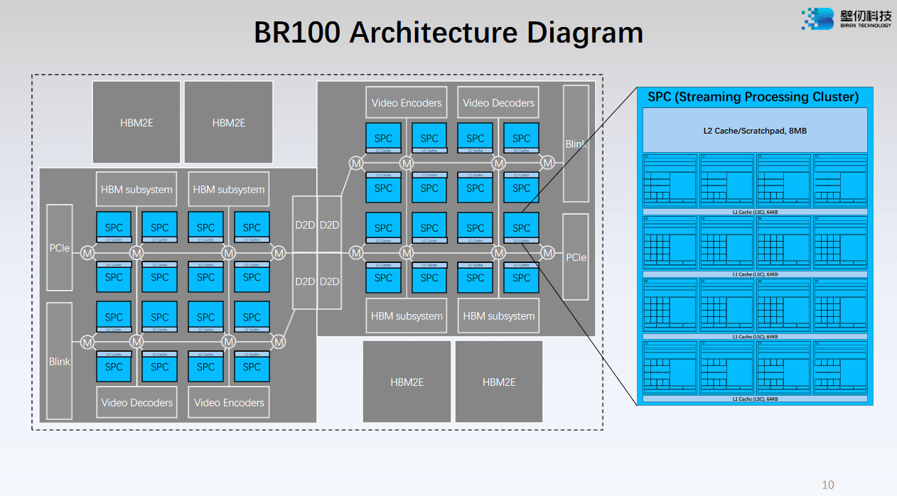
Similarities to SPR end there. BR100’s mesh connects SPCs rather than CPU cores, and SPCs are more like clusters of cores. A SPC’s block of L2 can be configured as a private scratchpad or private cache, while SPR’s L3 slices are always shared across a set of cores.
Unlike SPR, which places one core on each mesh stop, BR100’s mesh stops serve two SPCs. This decision is quite interesting because engineers typically place multiple processing elements on a single interconnect stop when they don’t expect each processing element to demand a lot of interconnect bandwidth. Examples include Alder Lake, which places quad core Gracemont clusters on a single ring stop, and Ampere Altra, which places two Neoverse N1 cores on a single mesh stop. N1 and Gracemont have moderate vector throughput and relatively large L2 caches, meaning that they shouldn’t be pulling a lot of bandwidth from the on-chip network.
But GPUs are known for being bandwidth hungry, and each SPC is packed full of gigantic matrix units. Biren is probably using very wide mesh links to handle interconnect traffic. They may also be using the SPC’s large 8 MB L2 to reduce off-SPC bandwidth demands. For perspective, AMD’s MI250X uses an 8 MB L2 to serve an entire GCD, so the BR100 enjoys much higher cache capacity across all its SPCs.
I’m very curious about how the mesh network will hold up when SPC L2 slices are used as a large, 256 MB unified cache. Biren says the high bandwidth cross-die connection allows both dies to be used like one GPU. Total HBM2E bandwith is 1.6 TB/s, so 896 GB/s of cross-die bandwidth should be adequate for striping one die’s DRAM accesses across all HBM2E controllers. However, cache bandwidth is typically several times higher than DRAM bandwidth. If cache accesses are evenly distributed across all L2 instances, the cross-die link could easily become a bottleneck.
Compute Architecture
BR100’s smallest building block is the EU, or execution unit. Compared to other GPUs, it emphasizes massive matrix throughput over just about everything else.

If my math is correct, Biren’s EUs have four times as much matrix throughput per clock as Hopper’s SM sub partitions. AMD’s CDNA2 is far behind and puts less emphasis on matrix multiplication performance. Hopper and CDNA2 both run at much higher clocks than Biren, but not by enough to close the gap in throughput per EU.
In other aspects, Biren’s EUs are less beefy. For example, they can’t track as much in-flight work as AMD and Nvidia. Low maximum occupancy means less latency hiding capability. Perhaps Biren is expecting most accesses to be serviced from L2.

BR100 also lacks several execution units present on AMD and Nvidia GPUs. The most obvious one is lack of FP64 support. Biren says they’re targeting GPGPU applications beyond machine learning, but lack of FP64 support will certainly exclude BR100 from some HPC applications. Biren’s presentation also made no mention of texture units. Nvidia’s Hopper still packs four TMUs in each SM. AMD’s CDNA2 still supports some “memory image” (texture) instructions, though CDNA2 does lack most of the texturing capability found in consumer GPUs.
Vector FP32 throughput on BR100 is also a tad weak compared to other GPUs shown at Hot Chips 34. Each EU only has 16 vector FP32 lanes. Combine low clocks with an EU count that’s not much higher than a MI250X’s, and we only get 16 TFLOPS of theoretical FP32 throughput. A Radeon 6900XT can bring more vector FP32 TFLOPs to bear, while drawing less power.

BR100 can still bring a lot of FP32 throughput to bear for compute applications, and should provide an advantage over using a CPU. For example, an AMD EPYC 7763 runing at its 2.45 GHz base clock would only provide 5 TFLOPS of FP32 compute. But compared to other GPGPUs, BR100’s vector throughput is unimpressive.
Memory Subsystem
Like other recent GPGPUs, BR100 uses a HBM setup that provides both high bandwidth and high memory capacity. Each die has two HBM2E stacks. Across the entire GPU, BR100’s HBM setup provides 64 GB of capacity and 1.6 TB/s of bandwidth. For comparison, GH100’s HBM3 setup gives it 80 GB of memory capacity, and 3 TB/s of bandwidth.
GH100 and BR100 actually have similar matrix throughput, which means BR100 will be more memory bandwidth starved if both GPUs have similar cache hitrates. However, BR100 does have a lot more cache, and should be less dependent on DRAM bandwidth than Nvidia’s Hopper.
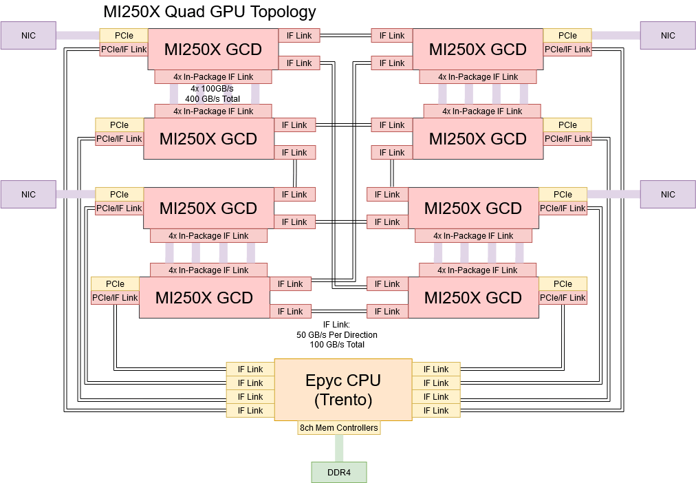
AMD’s MI250X technically has twice as much memory bandwidth and capacity as BR100, with 128 GB of HBM2E accessible at 3.2 TB/s. But MI250X doesn’t have enough cross-die bandwidth to expose all of its memory as a single pool, so AMD’s memory configuration can be more accurately described as two 64 GB pools, each accessible at 1.6 TB/s. To an application that can’t scale across multiple GPUs, MI250X would have similar DRAM capacity and bandwidth as BR100.
Connectivity
In our previous article on CDNA2, we noted how AMD implemented a complex topology to link eight MI250X GCDs in a HPC node. Biren also wants to place eight logical GPUs within one node, but takes a brute force approach and retains all-to-all connectivity. Every BR100 GPU gets a 64 GB/s link to every other GPU.
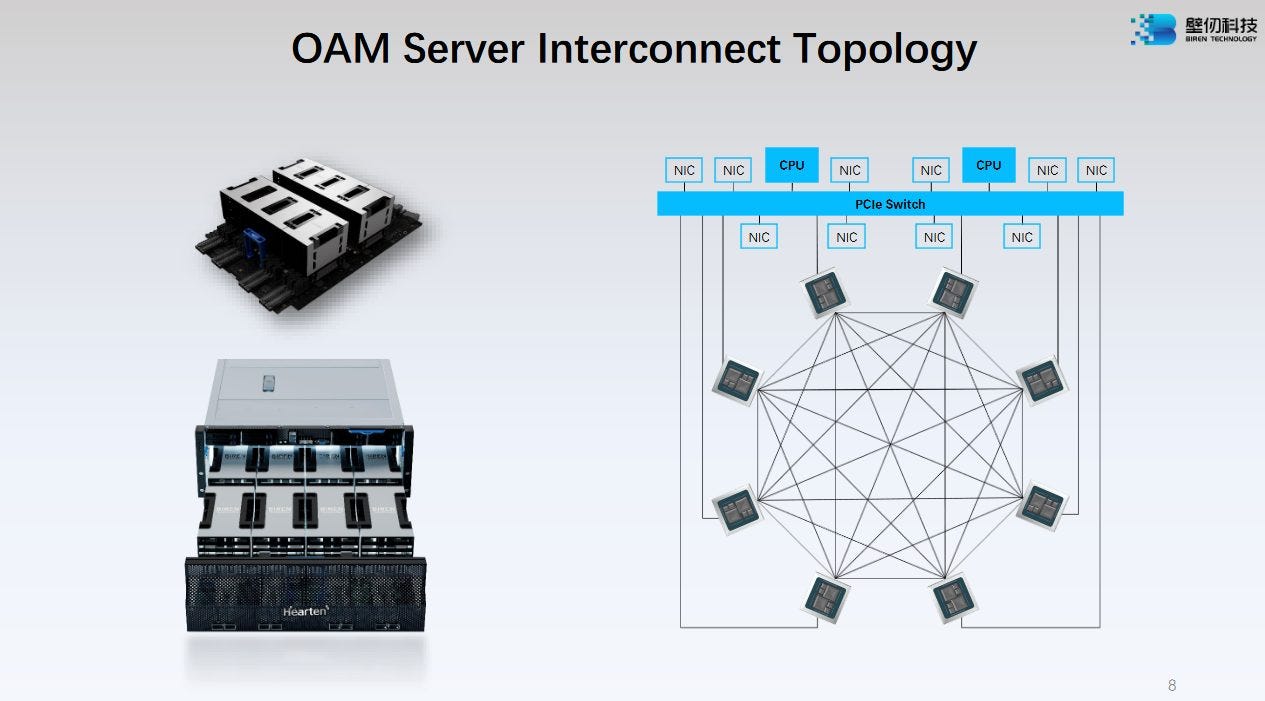
This simple topology ensures minimum communication latency between other GPUs within the node, because any other GPU can be reached in a single hop. You also don’t have to worry about multiple GPUs trying to reach another GPU over a single congested link. Compared to AMD, Biren has more external links, but less bandwidth per link. CDNA2’s 100 GB/s Infinity Fabric links give it more bandwidth between any two GCDs within a node, and GCDs implemented on the same die can communicate through a 400 GB/s link.
BR100 uses a 16x PCIe Gen5 to connect to the host. This link has CXL support, allowing hardware cache coherency to work across the CPU and GPUs. Finally, off-node connectivity is handled by NICs connected to a PCIe switch. We’re not sure if network traffic can be backed by GPU memory like on AMD’s CDNA2. The NICs are not directly connected to the GPUs, so network traffic is probably backed by CPU-side memory. I’m guessing the NICs are not 200 Gbps ones like in AMD’s HPC topology. Such high bandwidth NICs would put a lot of pressure on CPU-side memory bandwidth.
Conclusion
AMD’s CDNA2 focuses on the HPC market, with high FP64 throughput and lip service paid to lower precision matrix multiplication throughput. Nvidia’s Hopper and Intel’s Ponte Vecchio try to hit both fronts. With BR100, Biren focused on creating the most powerful machine learning GPU they could, while paying lip service to other GPGPU applications.
The result is a GPU that largely matches Nvidia’s H100 in matrix multiplication throughput, but falls behind in other categories. But theoretical figures are only one part of the story. BR100’s standout feature is a unique, CPU-like caching setup that can present a 256 MB unified L2 cache. Even AMD’s Infinity Cache in RDNA2 is only 128 MB in size. Considering BR100’s lower memory bandwidth and lower max occupancy, Biren is probably hoping to lean on the L2 cache to keep performance up. I’m still curious about whether Biren’s mesh links can keep up, but it’s fascinating that Biren is using an Infinity Cache like approach in the compute scene, while AMD and Nvidia have preferred to use smaller caches and a ton of DRAM bandwidth.
BR100 should provide Chinese customers with plenty of machine learning throughput, and give them an alternative to buying Nvidia or AMD products, considering recent restrictions. Customers using BR100 for other GPGPU applications will get some mileage out of BR100, assuming they don’t need FP64. Its vector FP32 throughput alone is still quite high compared to what you can get out of a CPU, while its flexible caching strategy and HBM should have no trouble keeping those execution units fed. But BR100 still puts AI first, and other non-matrix applications a distant second.
If you like our articles and journalism and you want to support us in our endeavors then consider heading over to our Patreon or our PayPal if you want to toss a few bucks our way or if you would like to talk with the Chips and Cheese staff and the people behind the scenes then consider joining our Discord.