
Nvidia’s RTX 4090 Launch: A Strong Ray-Tracing Focus

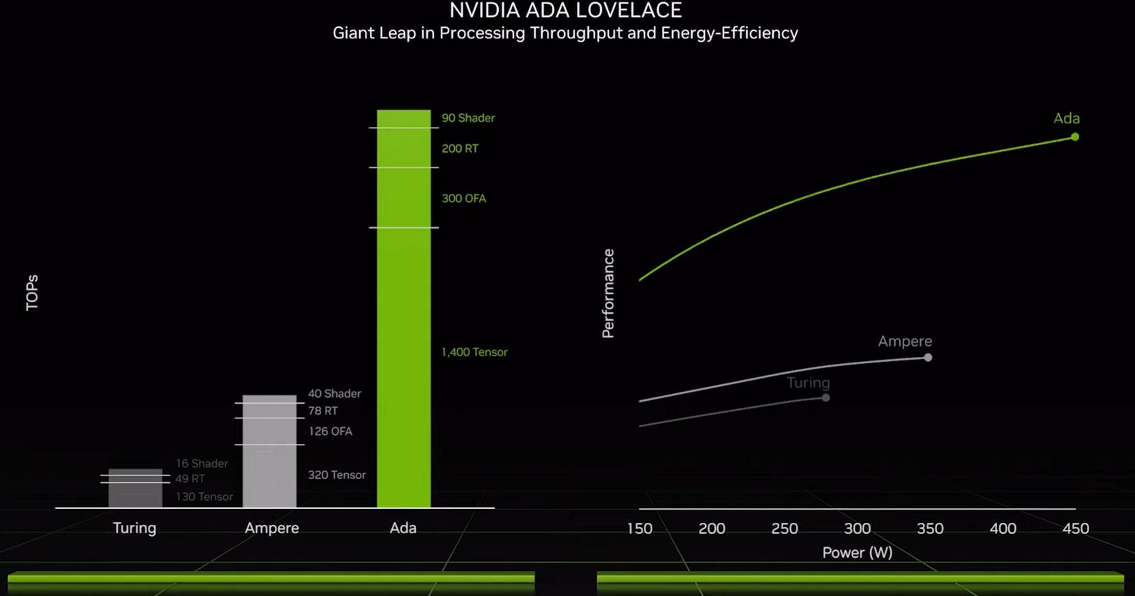
Recently, Nvidia announced their RTX 4000 series at GTC 2022. At a high level, Nvidia took advantage of a process node shrink to evolve their architecture while also scaling it up and clocking it much higher. The top end AD102 die found in the 4090 packs 76.3 billion transistors, which represents a whopping near 2.7x increase over the 28.3 billion transistors found in the RTX 3090’s GA102 die. SM count jumps from 82 to 128 with a hypothetical fully enabled AD102 die going up to 144 SMs. Even with the massive increase in parallelism, Nvidia has managed to increase boost clocks to 2.52 GHz. The result is a massive 450W card that requires a triple 8-pin power connector setup or one of the new 16-pin PCIe 5 power connectors.
Raytracing is the star of the show yet again. Nvidia has spent the last couple GPU generations betting hard on raytracing and the architecture behind RTX 4000, codenamed Ada Lovelace, continues this trend by evolving both Nvidia’s raytracing acceleration hardware along with the upscaling technologies designed to counter the framerate loss typically associated with enabling raytracing.
Increased Triangle Throughput
Ampere doubled the triangle intersection rate compared to Turing, and Ada Lovelace doubles it again. Box intersection rate was not mentioned. Triangle tests happen at the bottom level of a BVH, so Nvidia may be looking to avoid paying memory latency penalties by generating fatter BVH structures.
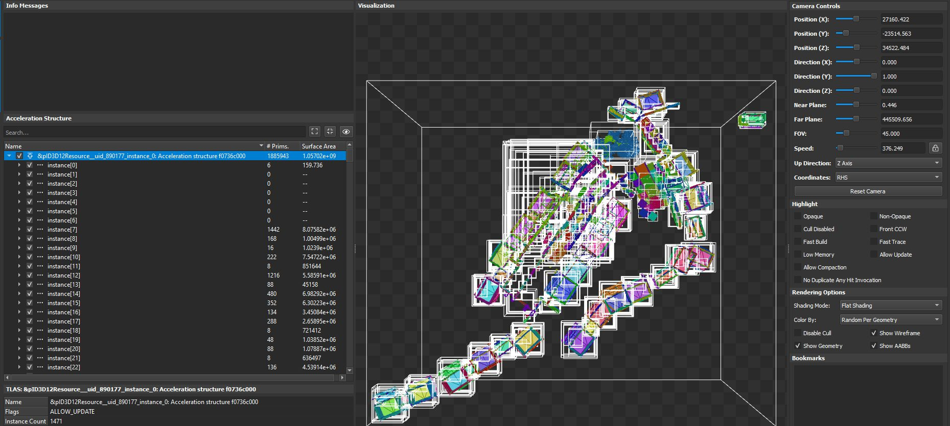
A BVH, or bounded volume hierarchy, is a tree that subdivides the volume in a scene. Each node in a BVH represents a rectangular volume within a 3D scene, and its children represent smaller rectangular volumes within that. Nodes at the bottom level of a BVH contain triangles that represent objects within a scene, and rays are tested against these triangles. Finally, corresponding shader programs are invoked depending on whether rays intersect these triangles.

You can imagine that if you subdivide a scene less, you’ll end up with larger bottom (leaf) nodes with more triangles each. The whole tree structure will appear fatter as well, with fewer levels. Creating a fatter tree structure cuts down on pointer chasing operations, but increases the number of arithmetic operations. Such a tradeoff can be very well suited to a GPUs, which tend to have very high cache latency but also very high math throughput. Nvidia is likely choosing to play to a GPU’s strengths by increasing triangle test throughput, and using that to avoid hitting cache latency.

Nvidia is actually already using very fat BVH structures in their existing raytracing implementations. On the GTX 1080, Nvidia generates a two level BVH structure. Each leaf node can have anywhere from hundreds to tens of thousands of triangles. The GTX 1080 doesn’t have RT hardware acceleration, but I don’t think Nvidia would develop a substantially different BVH generation code path just for Pascal. Like its successors with hardware RT acceleration, Pascal also has high math throughput and high cache latency. If anything, RT hardware would tilt the balance even further towards a fat BVH, because hardware acceleration for intersection tests would increase math throughput.

Looking further at Pascal, we can see raytracing data doesn’t fit within the relatively small 48 KB L1 texture caches. However, it does mostly fit within the 2 MB L2, and L2 latency is a distinct performance bottleneck. The SM Warp Stall due to “Long Scoreboard” corresponds to global memory accesses, and is responsible for half of all stalls. The next largest issues are “Wait” (execution latency), “No Instructions” (instruction cache miss), and “Not Selected” (execution bound, another warp was selected). RT hardware would cut down on all of these stall reasons. Dedicated intersection test hardware would require fewer instructions to do the same work, reducing instruction footprint. It would also be faster at intersection calculations, cutting down on execution latency and increasing throughput. All that would make the remaining elephant in the room (cache latency) more critical. Increasing triangle throughput could let Nvidia make the BVH even fatter, reducing its dependency on cache latency.
Finally, a fatter BVH might require less drastic modification as objects move around the scene. If a bounding box is big, an object can move further without leaving it. This wouldn’t be a consideration with applications like Blender, which spend a very long time rendering a single frame to very high quality. But it could be a factor for games.
Shader Execution Reordering
Nvidia also mentioned Shader Execution Reordering, which reorders work to achieve better parallelism when raytracing. Unfortunately, Nvidia is very vague on what this mechanism is. They describe it as being as big an innovation as out of order execution is for CPUs, but it’s extremely unlikely that Ada implements the kind of out of order execution we see in high performance CPUs. GPUs are built to keep many, many threads in flight to provide explicit parallelism, avoiding the problem of extracting instruction level parallelism from a single thread.
A more likely possibility is that their SMs have much deeper queues in their memory pipelines, letting them take advantage of more opportunities to coalesce accesses. An analysis of Turing’s RTX implementation suggested it was closely connected to the texture units, which already have hardware to reorder memory accesses.
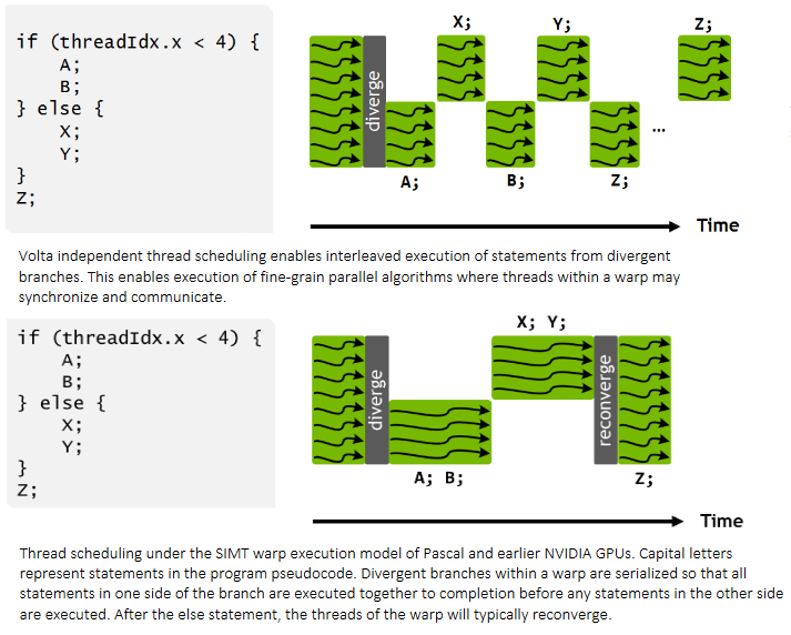
Another possibility is an extension of Volta-style independent thread scheduling. Volta introduced a scheme where each lane in a 32-wide warp can save its program counter in a vector register, letting the scheduler interleave execution of diverged warp parts. Usually, GPUs handle more than warp’s worth of invocations of the same kernel, so there’s a good chance multiple warps being tracked by the same SM partition are running the same kernel code. Maybe the scheduler can identify common instructions being executed by diverged chunks of multiple warps, creating new warps out of them. Then, diverged rays within a single warp might naturally find peer waves in other warps to reconverge with.
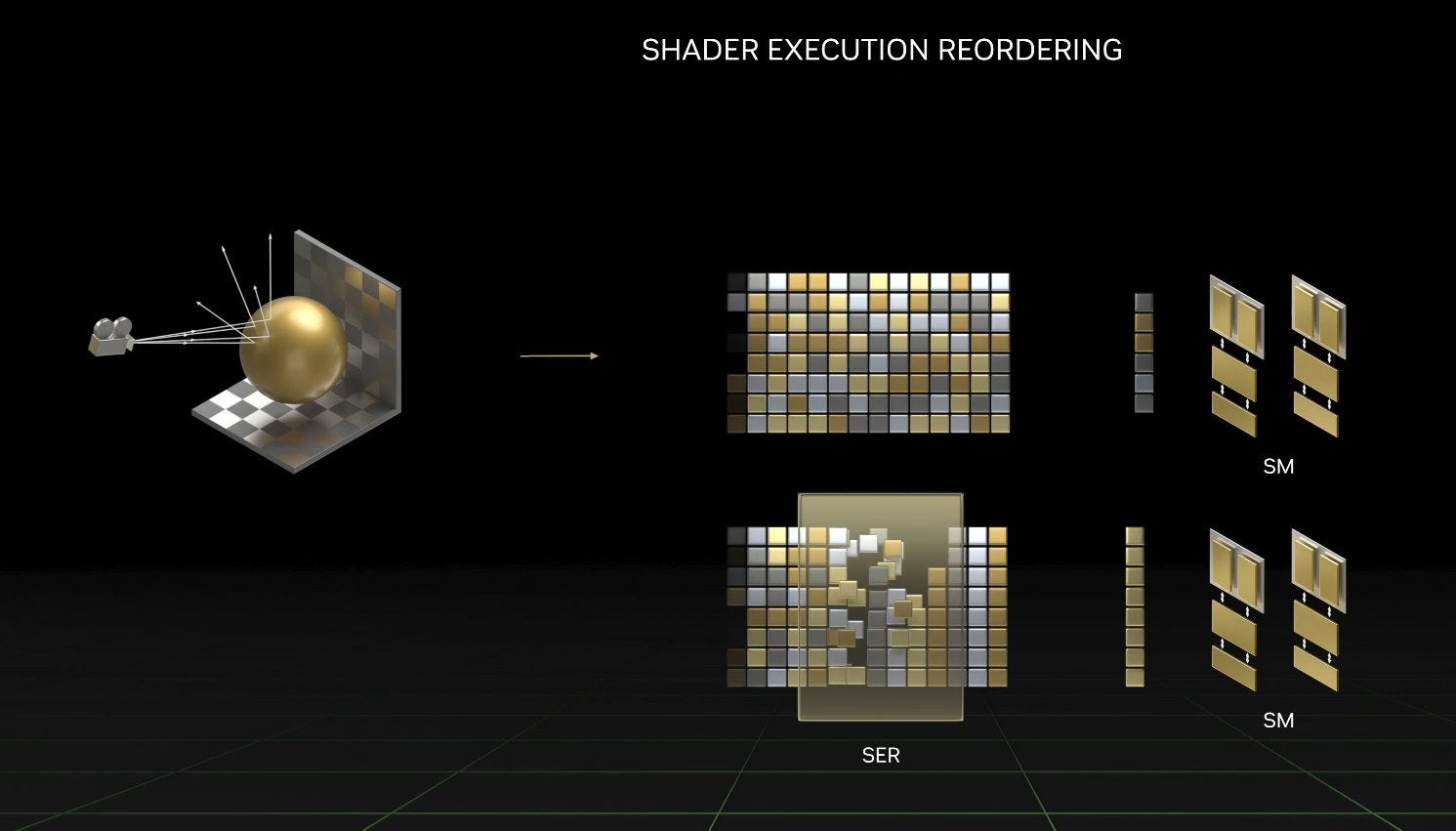
In any case, when companies use very vague statements to describe a new technique, we should always expect the most marginal architecture improvements possible. On that note, Nvidia may have simply improved how they organize rays into warps. Turing already organized rays into warps on the GPU-side. Adding special hardware to improve that process would be a natural evolution.
DLSS 3 – Hallucinating Harder
Despite Ada Lovelace’s improvements in raytracing, turning on ray traced effects will still cause a harsh framerate penalty. This has been true in previous Nvidia GPU generations as well, and Nvidia has attempted to counter this with DLSS. With DLSS, the GPU renders at reduced resolution and thus achieves higher framerate. Machine learning is then used to upscale the frames. DLSS 3 takes this process one step further by adding frame interpolation capability. That is, it generates entire fake frames between the real ones, allowing framerate increases beyond what’s possible by reducing resolution.
DLSS 3 does this by two frames to find out how pixels have moved. Generating motion vectors for pixels is also known as calculating optical flow. Like Turing and Ampere, Lovelace features a hardware “Optical Flow Accelerator” to speed up this process. With this OFA, Nvidia can calculate optical flow without throwing a lot of extra work at the shader array. Ampere’s OFA improves over Turing’s in several ways, including increasing the maximum supported resolution:

Nvidia has not provided any specifics about the OFA in Lovelace, beyond claims that it is significantly improved compared to Ampere, which is the basis for why DLSS 3 is not made available for Turing and Ampere.
Optical flow information is fed into a machine learning model along with two previous frames and motion info from the game engine. The ML model is then used to hallucinate an intermediate frame into place. This process is completely independent of the game’s processing loop and traditional rendering pipeline, meaning DLSS 3 can bypass CPU bottlenecks. If your CPU isn’t fast enough to figure out where objects will go within, say, the 6.9 ms interval between frames at 144 FPS, Nvidia’s DLSS 3 can use machine learning to fill in the gaps. While this approach increases framerate, it may negatively impact latency, because an intermediate frame is generated and presented after a future frame is already available.
For this rapid hallucination to work well, Nvidia needs a lot of processing power, and that’s where tensor core improvements come in. Lovelace therefore doubles per-SM tensor throughput, with a 16:1 ratio of FP16 tensor to FP32 vector throughput compared to Ampere’s 8:1 ratio. Add in SM count and clock speed increases, and Ada Lovelace can provide massive matrix multiplication throughput for machine learning inference. DLSS 2 already used optical flow information along with a previous frame to calculate a current frame. But a massive increase in processing power likely made it feasible to interpolate a completely new frame, as well as upscale a current frame. Previous generation cards likely lack the processing power required for this, explaining why DLSS 3 is only available on Lovelace cards.
Rasterization Improvements
Games that take advantage of hardware accelerated raytracing can add some flashy effects, but rasterization is still core to gaming today. Not all games support raytracing, and most of the ones that do support raytracing still rely on rasterization to render the bulk of the scene. Even when rendering at reduced resolutions with hardware acceleration, we still don’t have enough raytracing power to render frames in real time using raytracing alone. Therefore, the RTX 4000 series gets a rasterization performance boost too, mostly from scaling up the GPU and clocking it higher.
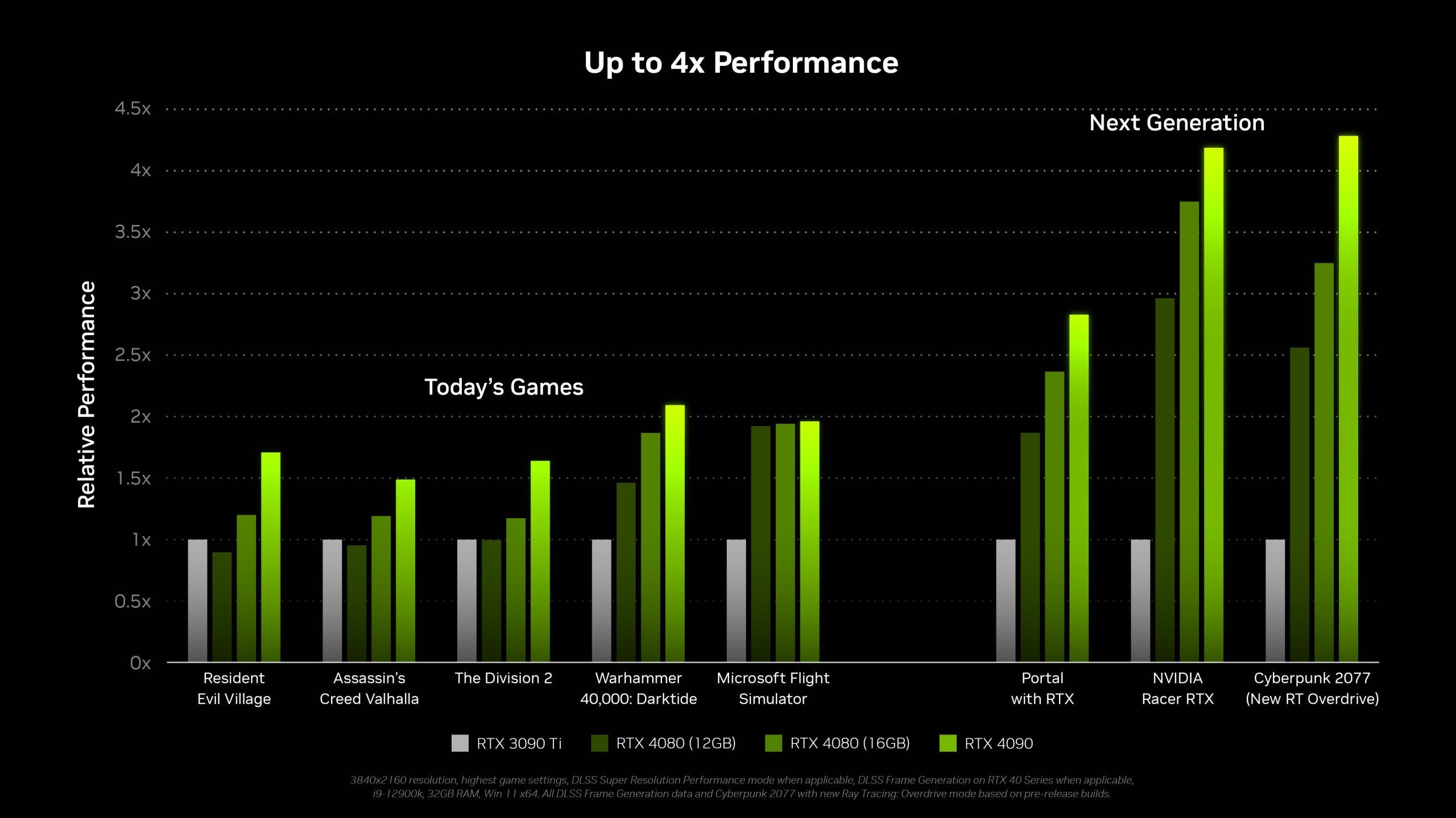
With these SM count and clock speed increases, RTX 4090 has double RTX 3090’s FP32 vector throughput. Assassin’s Creed Valhalla doesn’t use DLSS or raytracing, making it a useful data point for rasterization performance. The RTX 4090 achieves a 50% performance boost over the 3090 Ti in that game.
A 50% performance boost for a 100% increase in theoretical FP32 throughput might not sound very impressive, but we should remember that performance gains rarely scale perfectly with increases in theoretical throughput. Most applications are simply not bound by compute power all of the time. AD102 also uses a 384-bit GDDR6X setup, just like GA102, and likely implements its massive increase in FP32 throughput without an equally massive increase in memory bandwidth. In order to feed the execution units, AD102 is rumored to implement a gigantic 96 MB L2 cache. This is almost as big as the 128 MB “Infinity Cache” found on AMD’s Navi 21, and likely serves a similar purpose. Still, caches aren’t perfect and in some cases there might be enough L2 misses to create a memory bandwidth bottleneck.
In any case, a 50% performance boost in rasterization is a large increase, and we look forward to seeing if it holds up in other games.
What’s AMD Doing?
AMD has not announced concrete details on their RX 7000 (RDNA 3) GPUs, besides claiming a 50% increase in performance per watt, and a move to TSMC’s 5 nm process. However, several LLVM patches provide hints about RDNA3’s direction.
For raytracing, RDNA 3 adds a new LDS instruction opcode to assist BVH traversal. AMD is likely using a stack to perform BVH traversal, and is keeping the stack in the LDS. Existing RT kernels on Navi 21 already have some LDS access instructions, so AMD may already be using the LDS to store a stack of pending nodes to visit. Dedicated instructions would help speed up access to this stack, and possibly reduce the number of instructions the SIMDs would have to crunch through when doing stack operations related to BVH traversal. There might be other improvements as well, but as of now we don’t know more.
RDNA 3 also introduces VOPD instructions. VOPD stands for Vector OPeration, Dual. Just as the name suggests, two operations are packed into a single instruction for dual issue, allowing AMD to double throughput for some common instructions without the area expense of implementing more SIMDs.

VOPD will likely enable massively increased FP32 throughput on RDNA 3 GPUs, without a correspondingly massive increase in CU count and clock speed.

Of course, this isn’t as flexible as increasing SIMD count. Certain less common operations can’t be issued in both VOPD opcode slots. AMD will be trying to feed significantly more execution power without duplicating SIMD-private resources, like the wave scheduler and register file. Certainly some of the circuitry got beefed up to allow dual issue capability, but it doesn’t look like AMD made any particularly expensive changes. The register file remains quad-banked, and conflict detection logic is unable to resolve bank conflicts for a single operand position.

So, there are significant restrictions around when dual issue can work. Bank conflicts between registers fetched for the same operand position are not allowed. Dual issued instructions have to write their results back to different pairs of banks. Finally, the two instructions together cannot have more than two scalar register inputs, and immediate values count as scalar inputs. It’ll be interesting to see how well AMD can take advantage of the extra throughput.
Interestingly, Nvidia has used a similar strategy to double FP32 throughput in Ampere. They added a second 16-wide FP32 unit to their SM sub-partitions, while leaving register file bandwidth untouched. So while an Ampere SM on the surface has as much theoretical FP32 throughput per clock as a Pascal SM, the Ampere SM will have a harder time feeding its FP32 units due to register bandwidth restrictions.
Zooming back up, AMD seems to be taking a more reserved approach to raytracing, while aiming for large rasterization gains via cheap FP32 lane spam. Of course, we don’t have all the details yet, so we look forward to seeing exactly what AMD comes out with later this year.
Final Words
Nvidia’s Ada Lovelace is a massive jump over Ampere. The top end SKUs feature huge SM count increases and significant increases in clock speed, so performance is predictably much, much higher in any scenario. Ada Lovelace’s biggest gains will show up in titles that use both raytracing and DLSS 3, but Nvidia’s latest GPU should be a monster in pure rasterization workloads, even if rasterization wasn’t a top priority.
If you like our articles and journalism and you want to support us in our endeavors, then consider heading over to our Patreon, or our PayPal if you want to toss a few bucks our way. If you would like to talk with the Chips and Cheese staff and the people behind the scenes then consider joining our Discord.