
How Quickly do CPUs Change Clock Speeds?

We often see very high clock frequencies listed for our CPUs. But CPUs don’t run at maximum clock all the time in order to reduce power consumption and heat generation. They also can’t instantly go from one clock speed to another, because power delivery circuitry needs time to ramp up voltage and deliver higher current. In this article, we’re going to look at how fast various CPUs can go from idle clocks to higher frequencies. Let’s start with the results, then finish with how we conducted this little experiment.
Time to Max Boost
Here’s a quick overview of how some CPUs take to hit their maximum boost frequencies. Alone, this graph doesn’t tell the whole story, because a lot of these CPUs level off at intermediate frequencies well above their idle clocks before boosting all the way.

Now, let’s dissect clock ramp behavior on these CPUs.
AMD’s Zen 3
Zen 3 debuted toward the end of 2020, and is about to be replaced by Zen 4. But right now, it’s still the newest widely available AMD architecture. In mobile form (Cezanne), we see very fast frequency ramp behavior, reaching 3.7 GHz in just a couple milliseconds. However, we didn’t see the core boost to 4.4 GHz. Perhaps it would do so after a while, but the test wasn’t run for enough iterations.

Still, 3.7 GHz is fast enough to give a decent user experience.
AMD’s Zen 2
AMD’s Zen 2 architecture debuted in 2019, and was implemented across mobile, desktop, and server form factors. In desktop (Matisse) form, the core starts at 1.7 GHz and takes somewhat longer to boost, only reaching 4.3 GHz after 16 ms. On the 3950X, the best binned cores level off at 4.3 GHz for a millisecond before hitting 4.7 GHz after 17.45 ms. Clock ramp behavior Zen 2 is slower than on Zen 3, but still quite fast considering 17.45 ms is a single frame at 57 FPS.

Mobile Zen 2 (Renoir) is even more impressive, and gets to 4.3 GHz in just over 9 ms. To save power, Renoir also starts at a lower 1.4 GHz clock speed.
The Ryzen 9 3950X was tested on the ASRock X570M Pro4, and the Ryzen 4800H was in an Eluktronics RP-15 laptop.
Intel’s Skylake
Skylake came out in 2015, but remained relevant well past 2020 thanks to Intel’s inability to bring a newer architecture to the desktop market for quite a few years. Intel debuted a technology they called “Speed Shift” in Skylake, which hands off processor power state control to the CPU instead of having the operating system ask for transitions. The Core i5-6600K shows this feature off quite well, and reaches its maximum boost clock of 3.9 GHz after just 5.62 ms.
Kaby Lake is a refresh of the Skylake architecture in 2017, but shows very different behavior and takes 31.5 ms to reach 2 GHz. Its maximum boost clock of 4.5 GHz isn’t reached until 62.54 ms.

I suspect this has something to do with the i7-7700K being implemented in an OEM system. The motherboard is a HP 802F with the Intel C236 chipset. Meanwhile, the i5-6600K was installed in the MSI Z170A Gaming Pro Carbon, a pretty average enthusiast board that shouldn’t bring any strange surprises.
AMD’s Piledriver
Piledriver is an AMD architecture from 2012. Normally, the FX-8350 shows clock ramp behavior similar to that of client Haswell, taking close to 80 ms to reach its maximum boost clock. However, Piledriver does reach a respectable 3.4 GHz after 47 ms, meaning the CPU should feel a bit more responsive than its time-to-max-boost would suggest.
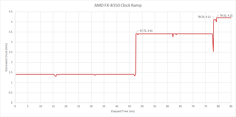
If the Windows power plan has minimum CPU state set to 100%, the FX-8350 will stay at around 1.35V even when idle. In this mode, Piledriver shows extremely fast boosting behavior, shooting from 1.41 to 4.1 GHz in less than a fifth of a millisecond, and reaches its maximum boost clock of 4.2 GHz in a little over a millisecond. This suggests most of the delay in clocking up comes from waiting for voltages to increase.

The FX-8350 was installed in a Gigabyte GA-990FX-Gaming board.
Intel’s Haswell
Intel’s Haswell architecture from 2013 helped cement Intel’s already strong lead across desktop and server markets. Implemented on Intel’s 22nm FinFET process, it introduced AVX2 and offered increased cache bandwidth over its predecessors. On client implementations, Haswell’s boosting behavior is similar to other CPUs of its time. Desktop Haswell hits a moderate 2.5 GHz after 31 ms, and only reaches high clocks after 60 ms. Mobile Haswell has even more conservative boosting behavior, reaching 2 GHz after 47 ms and maximum clock after 79 ms.

Hitting moderate clocks early should let Haswell feel a little more responsive than the time-to-max-clock figures would suggest. Still, it’s nowhere near as fast as “Speed Shift” on Skylake.
The Core i7-4712HQ was tested in a Dell Precision M3800 laptop, and the i7-4770 was installed in an Asus Q87M-E board.
Intel’s Old HEDT: Sandy Bridge and Haswell
Long long ago, in a galaxy not so far away, Intel dominated the high end desktop market. If you wanted more than four cores, you paid Intel and were happy to do so. Looking back at those days (which were glorious for Intel), we can see that Intel’s HEDT chips reached intermediate clocks pretty quickly, but took their sweet time to hit maximum boost clocks. The Sandy Bridge based Xeon E5-1650 reaches its base clock of 3.2 GHz in about the same time it takes client Haswell to hit maximum boost clocks. Then, it waits for almost half a second before going up to its 3.8 GHz single core turbo frequency. HEDT Haswell is somewhat better and hits maximum clock speeds in around a third of a second, but I tested a pretty low clocking Haswell SKU here.

Unlike Intel’s desktop and mobile platforms, which typically idle at 800 MHz, the HEDT chips start at a slightly higher 1.2 GHz. I wonder if the very long clock ramp times we see here are deliberate, and meant to keep power consumption down for short tasks.
The Xeon E5-1650 was in a HP 1589 motherboard with a C602 chipset, while the E5-2630 v3 was in a Dell 0K240Y with a C612 chipset. I’m sure these motherboard names make a lot of sense to you, because they clearly made sense to Dell and HP.
Low Power Intel: Goldmont Plus
Goldmont Plus is a low power Intel architecture introduced in 2017. It’s a 3-wide architecture with out-of-order execution and more powerful than the Atom chips of the early 2010s, but is still not meant to compete on the desktop. Unlike the contemporary Skylake architecture, it doesn’t seem to implement “Speed Shift” and takes 47 ms to hit 2.6 GHz.
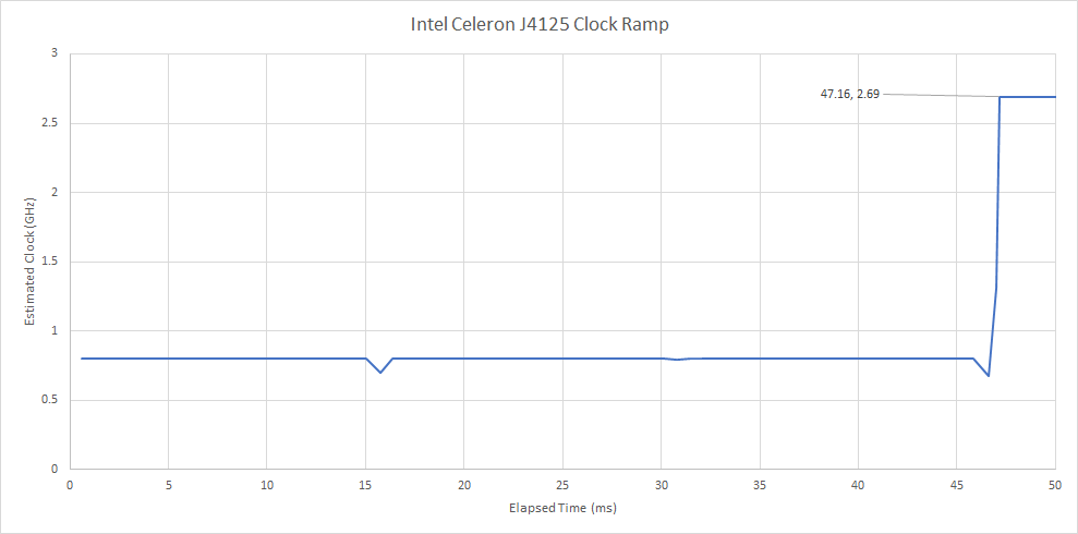
Goldmont Plus was tested on a GK41 small form factor PC from some “Coofun” brand. Don’t ask any more questions. It sounded like a good idea at the time.
Qualcomm Snapdragon 670
The Snapdragon 670 is a midrange cell phone SoC from 2018 with two Cortex A75 cores, and six of everybody’s favorite Cortex A55 cores. The A75 cores reach 2 GHz, while the A55 cores hit 1.7 GHz. Frequency ramp is quite fast on the A75 cores, while the A55 cores take a bit longer to reach their maximum clock speeds. Strangely, the A55 cores increase clocks faster when the phone is plugged in, while the A75 cores ramp frequency faster on battery power.

Another interesting detail is that the A55 cores start at a very low 600 MHz, while the A75 cores start at just above 800 MHz.
The Snapdragon 670 was tested in a Pixel 3a.
Qualcomm Snapdragon 821
Qualcomm’s Snapdragon 821 is probably best known for not being the Snapdragon 810. However, it’s quite a unique chip in that both the high performance and low power cores actually use the same Kryo architecture, though with different cache setups. Kryo is a 4-wide out-of-order core with four ALUs and reasonably deep reordering capacity, so the Snapdragon 821 has some of the biggest “little” cores of its time. Sadly, Qualcomm was very bad at implementing caches, but that’s a story for another day.
Little Kryo behaves similarly regardless of whether the phone is running off battery, or plugged in with the battery fully charged. Either mode results in the core taking over 200 ms to reach 1.59 GHz after gradually boosting in steps. Battery mode just seems to bring idle frequency down to a very low 300 MHz. On AC power, they idle at 600 MHz.

Big Kryo has similar idle frequency differences, but clock ramps much faster when running off AC power. It reaches 2.34 GHz in under 20 milliseconds if the phone is fully charged and connected to a power source, but takes almost 400 ms to do so on battery. This behavior might be deliberate, to prevent the core from drawing a ton of power to complete very short tasks. Funny enough, little Kryo actually clocks a hair higher than big Kryo from 100 to 300 ms when the phone is running on battery.
The Snapdragon 821 was tested in a LG G6.
Zhaoxin’s LuJiaZui
As a bonus, we tested Zhaoxin’s LuJiaZui architecture, in the KX-6640MA. Data for this CPU was gathered using an older version of the test, which uses a keypress to start data collection rather than sleeping for five seconds. As it turns out, the keypress itself could take a few milliseconds to get delivered to the program, resulting in slightly less accurate measurement. Still, there’s enough data to show that LuJiaZui has reasonably fast clock ramp behavior. It increases clocks faster than Goldmont Plus, but not as fast as Zen 3, or Skylake.

Methodology
Our test executes a known number of dependent integer additions, which execute at one per clock cycle on the vast majority of CPUs. If we time how long it takes to execute a certain number of dependent additions, we can use that as a proxy for how many CPU cycles have elapsed, and thus calculate clock speed. CPUs can’t change clock speeds instantly, but a lot of them can do so faster than we can accurately measure with standard timing APIs like gettimeofday or ftime.

Therefore, we’re using RDTSC (read TSC, or timestamp counter) on x86, or CNTVCT_EL0 (counter timer virtual count register) on ARM to measure time differences. We repeat the process above, and hopefully see increased clock speeds (smaller RDTSCor CNTVCT_EL0 increments) after a few iterations. Then, we separately determine how rdtsc or cntvct_el0 increments correspond to real time differences by measuring a large time difference (about 2 seconds) with both gettimeofday and rdtsc/cntvct_el0. This setup lets us get accurate timings below a millisecond, though timing accuracy will eventually be limited by rdtsc or cntvct_el0 overhead.
Another curious note is that CNTVCT_EL0 on ARM CPUs offers somewhat less precision than RDTSC on x86 CPUs. x86 CPUs tend to increment the timestamp counter at base clock. For example, the FX-8350’s timestamp counter will increment four times every nanosecond, corresponding to its 4 GHz base clock. The Snapdragon 670 and Snapdragon 821 cores increment CNTVCT_EL0 roughly once every 50 nanoseconds.
If you like our articles and journalism and you want to support us in our endeavors then consider heading over to our Patreon or our PayPal if you want to toss a few bucks our way or if you would like to talk with the Chips and Cheese staff and the people behind the scenes then consider joining our Discord.