
Hot Chips 34 – Intel’s Meteor Lake Chiplets, Compared to AMD’s

During a presentation at Hot Chips 34, Intel detailed how their upcoming Meteor Lake processors employ chiplets. Like AMD, Intel is seeking to get the modularity and lower costs associated with using chiplets. Unlike AMD, Intel has made a different set of implementation choices that makes Meteor Lake specifically suited for tackling different client segments.
High Level Strategy
Intel’s client offerings throughout the last decade targeted different market segments with different monolithic dies. These client dies are not particularly large, so monolithic designs made sense for some time. But Intel has been increasing core count, introducing hybrid architectures, adding more SoC capabilities (like Thunderbolt support), and pushing as hard as ever on the integrated graphics front. That means a dramatic increase in the number of possible configurations, and at some point, going with tiles would let Intel fab a lower number of unique dies. Splitting the design into tiles would thus help streamline production.

That brings us to Meteor Lake. Meteor Lake is split into four tiles. A CPU tile contains CPU cores and their cache, much like AMD’s CCDs. The integrated GPU gets its own tile. A SoC tile contains most of the functionality found in the system agent in current Intel client CPUs. Finally, an IO extender tile is connected to the SoC tile. All of the tiles are mounted on top of a passive base die, which connects the tiles and handles power delivery.

This approach provides a lot of potential for tile reuse as Intel customizes chips for different client market segments. For example, a core tile with six P-cores and two E-core clusters could see use in a variety of form factors. When paired with a SoC tile that emphasizes PCIe lanes, it can go in midrange desktop chips. Alternatively for laptops, it can be paired with a SoC tile that has an image processing unit for better battery life with heavy webcam use.
Contrasting with AMD’s Approach
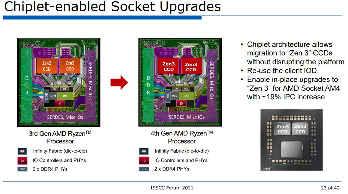
In contrast, AMD’s chiplet approach allows die reuse across desktop and server segments, but not so much across desktop and mobile right now. Plain on-package links through the PCB are cheap and allow long reach, but aren’t the best for bringing down power consumption. So, AMD currently uses separate monolithic dies to target mobile segments.
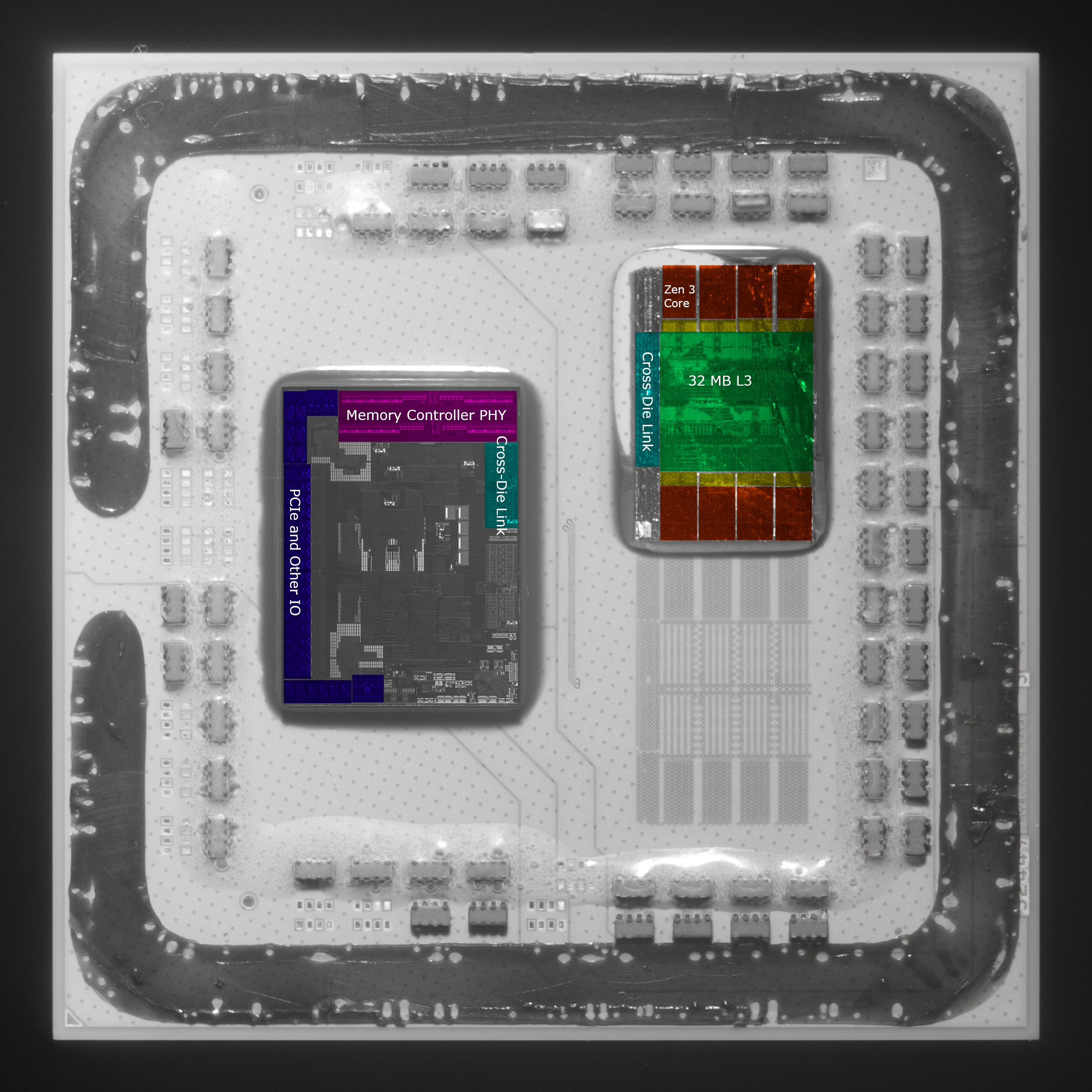
Meteor Lake’s packaging solution is almost definitely more expensive. Intel needs to include a separate base die. Scaling up Meteor Lake will be more difficult – including larger CPU tiles or more CPU tiles would require larger base dies. In exchange, Intel’s design can achieve higher IO density and use less power to move data between tiles. As we can see, die to die link design is heavily tied to both companies’s approaches. Let’s have a closer look at that.
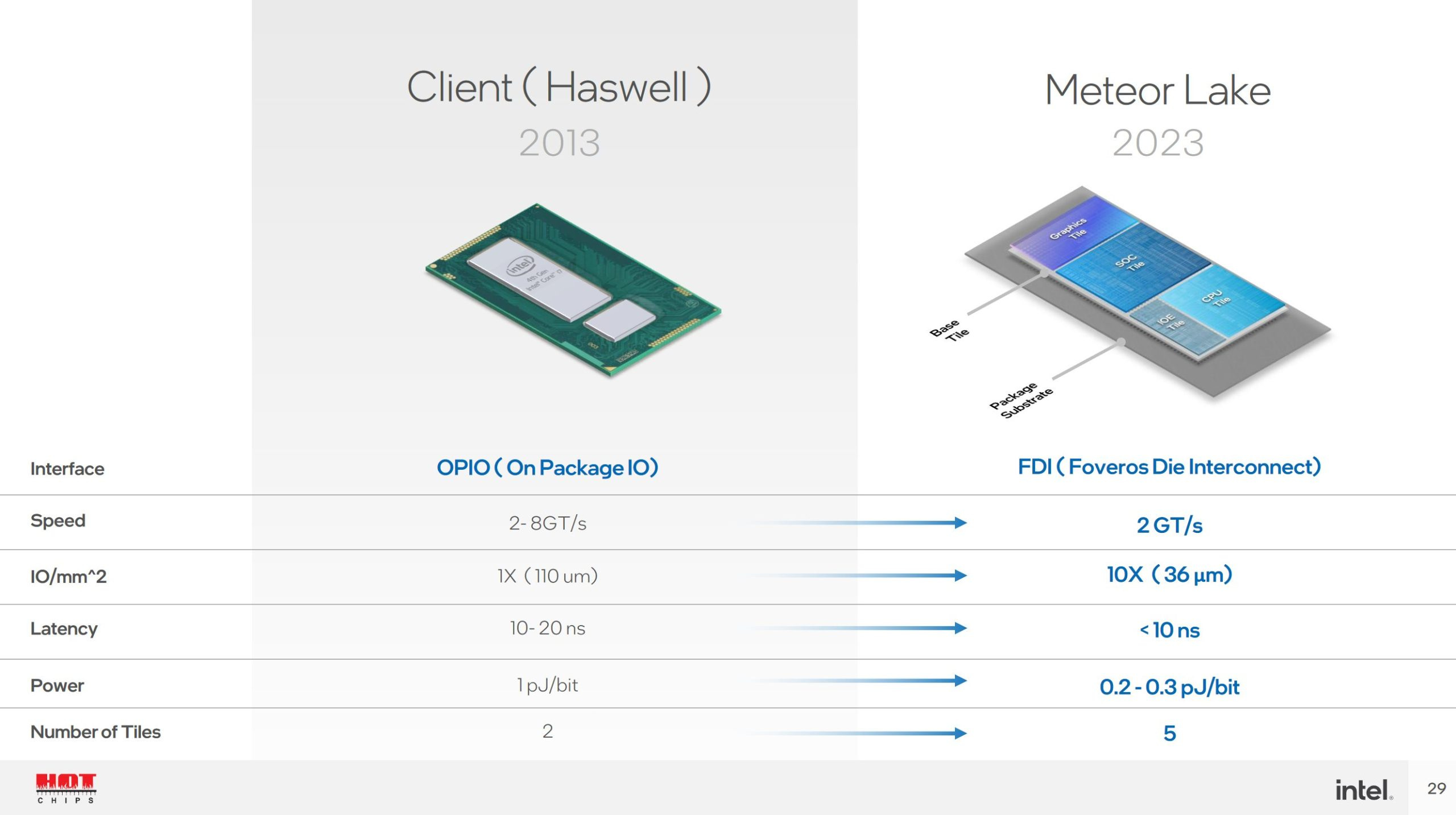
That Die to Die Interconnect
Intel calls their die to die link “Foveros Die Interconnect” (FDI). Its higher IO density should allow smaller packages in space constrained ultrabook boards. Also, power consumption is critical in battery powered designs and there’s no doubt that FDI is far better suited for hitting the mobile segment than AMD’s plain on-package interconnect. AMD stated that Zen 1’s die-to-die Infinity Fabric links had a power cost of 2 pJ/bit, and their Zen 2 launch slides indicated that Infinity Fabric could move data with 27% less power per bit. Obviously we don’t know how much of that power reduction came from optimizing the cross die link compared to other logic, but it’s reasonable to assume that AMD’s die-to-die transfers cost as much power (or even more) than Intel Haswell’s OPIO link.
Surprisingly though, Intel doesn’t advertise a big latency advantage. Intel’s slides are extremely vague, only showing that latency is somewhere under 10 ns. AMD also claims to achieve under 10 ns latency, using plain on-package links.
The total round-trip latency from the CCD to IOD and back, including the digital control logic is 13 FCLKs, or less than 9 ns
AMD Chiplet Architecture for High-Performance Server and Desktop Products, ISSCC 2020
More specifically, AMD says latency is 13 Infinity Fabric (FCLK) clock cycles. The paper discusses both Matisse and Rome (Zen 2 in desktop and server form, respectively), and appears to be assuming 1.46 GHz FCLK to get that 9 ns figure. That lines up with running DDR4-2933 in coupled mode. Latency would be lower on desktops, which often run faster DDR4. At 1.6 GHz FCLK clock, latency would be closer to 8 ns. With FCLK pushed to 1.8 GHz, which is possible for many Matisse chips, 13 FCLKs would be 7.22 ns. Of course, Intel’s <10 ns figure could indicate a real figure as low as 2-3 ns. But if Intel could bring latency down to that level, they’d probably show it off more prominently.
Bandwidth figures are also unclear. Intel states FDI can do 2 billion transfers per second, without specifying how wide each transfer is. Based on how Intel’s employing FDI though, I suspect bandwidth is not significantly higher than OPIO or IFOP.
Tile Layout, and Communication Protocols
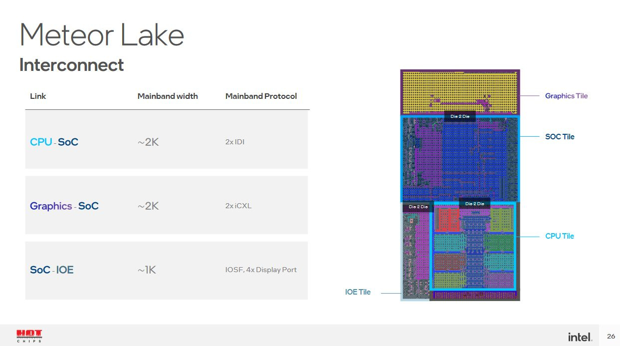
We can also examine where Intel’s using FDI to get an idea of its performance characteristics. None of the FDI links appear to be in high bandwidth, latency sensitive paths. The link between the CPU tile and SoC tile will mostly see L3 miss traffic, which should only be in the tens of GB/s, with hundreds of cycles of latency. The SoC tile to IO extender tile will probably handle PCIe traffic, which has even lower bandwidth and higher latency.
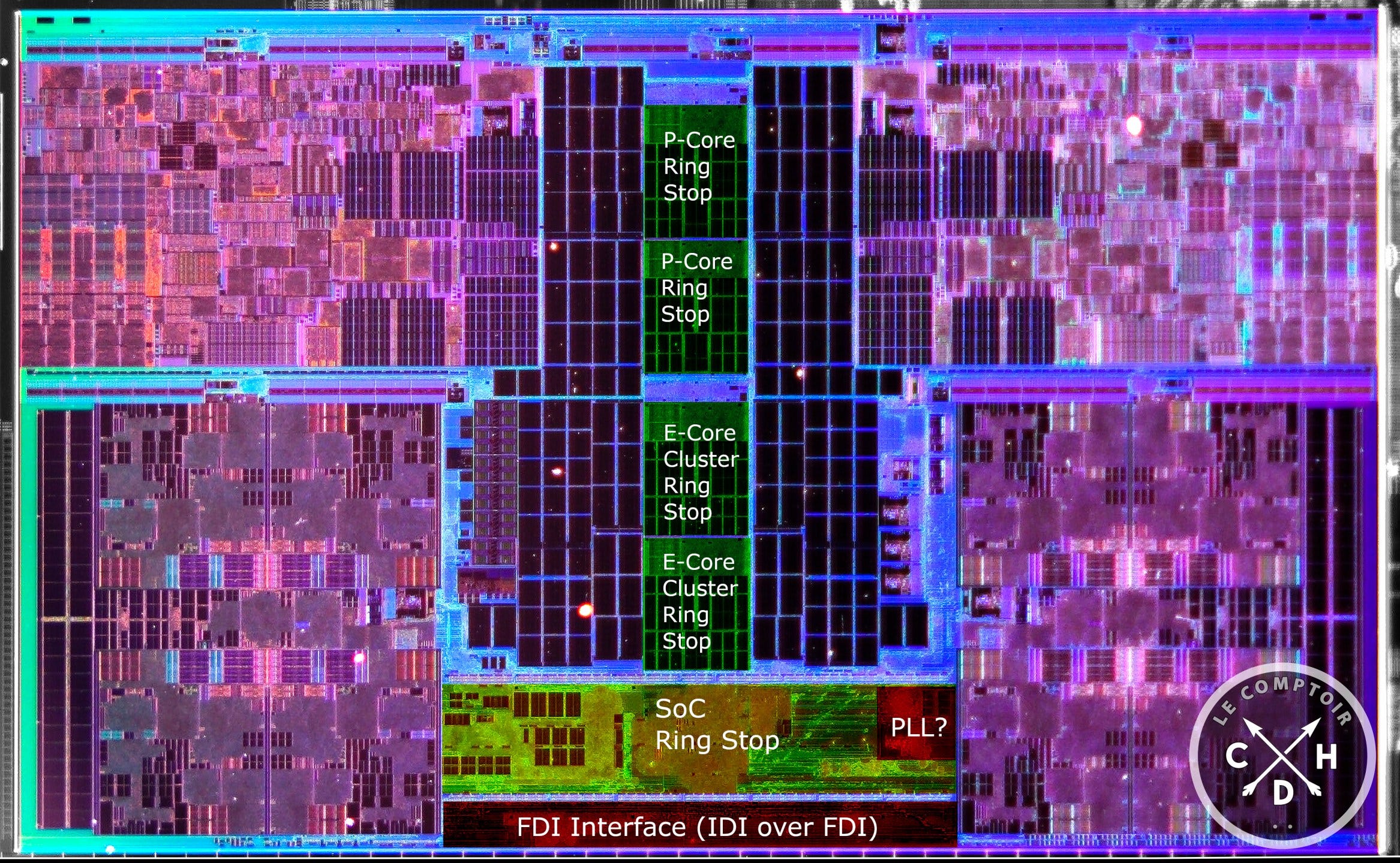
An interesting thing to note is that Meteor Lake places the iGPU far away from the CPU’s L3 cache, on the other side of the SoC tile. Previous Intel designs put the iGPU on a ring bus stop, where it naturally shared the CPU’s L3 cache. On the other hand, if Meteor Lake’s iGPU wants to hit the CPU’s L3, it has to take a long path through the center SoC tile. Taking that long path for every request coming out of the iGPU doesn’t make sense. So I believe that the iGPU tile likely behaves just like the CPU tile – that is, the iGPU to SoC link will only see iGPU to DRAM traffic. I don’t think the L3 is shared like in previous Intel designs.
Another hint is in the communication protocols used, so let’s take a detour to discuss that. Intel says the CPU and SoC tiles communicate with the IDI protocol, while the iGPU tile uses an iCXL protocol to talk to the SoC. The SoC and IO extender tile are connected via IOSF (Integrated On-chip system Fabric) and DisplayPort. We all know what DisplayPort is, and IOSF shares a ordering model with PCI. The IO extender tile probably has a PCIe controller and some DisplayPort PHYs, and the cross-die connection does little more than feed those interfaces. IDI and iCXL are much more interesting though, and could give us hints about how the iGPU interacts with the CPU tile.
IDI, or In-Die Interface, first appeared in Intel’s Nehalem architecture, where it connected cores to the uncore’s Global Queue and L3. Since then, IDI has continued to serve as the main protocol on Intel’s ring bus, with various updates and improvements over time. It uses a MESIF cache coherence protocol, meaning that a cache line’s state can be Modified, Exclusive, Shared, Invalid, or Forward. The IDI protocol itself seems to be quite complicated, with different sets of packet types destined for specific queues in L3 slice control logic. For example, each L3 slice has an Ingress Request Queue (IRQ). When an IDI packet from a core arrives at the L3 slice it’s addressed to, it’ll be pulled off the mesh or ring and added to the IRQ. Packet types represent very specific memory access requests from cores, and let the L3 slice controller maximize performance while maintaining cache coherency.

Other queues include the Ingress Probe Queue, which handles snoops, and the Writeback Queue, which handles writebacks from cores. In summary, IDI is an internal protocol meant to handle mesh or ring bus traffic, which includes high bandwidth, low latency communication between CPU cores and the L3 cache. Previous generations of Intel iGPUs used the IDI protocol, naturally making them an agent of the L3 cache just like the CPU cores. Documentation for Haswell’s iGPU supports this – there’s an IDI hash mask used by the iGPU driver to configure eDRAM caching.
But Meteor Lake’s iGPU swaps over to iCXL, an internal implementation of Compute Express Link (CXL) that doesn’t use a PHY. CXL is based off of PCI Express, and like PCI Express, is meant to connect a CPU to IO devices. Compared to PCIe, CXL 3.0 allows better hardware handling of cache coherency, adds latency-optimized message formats (flits), and can accept a wider variety of devices by implementing three sub-protocols – CXL.io, CXL.cache, and CXL.mem. These sub-protocols are meant for generic devices, coherent accelerators like GPUs, and memory expansion devices respectively. If you look through CXL.cache request types, you can see that some have vague equivalents in IDI. But CXL is not the same as the IDI protocol, and isn’t meant to connect processing cores to their caches.

Some of the CXL packet types have vaguely similar counterparts in IDI, but these similarities mostly show up in IDI packets destined for the Remote Request Queue (RRQ), which handles UPI requests from a remote socket. Packet types used by cores to access L3 (DrD, Crd, RFO, etc) are conspicuously absent. Another difference is that CXL uses a basic MESI coherency protocol. It doesn’t have the Forward state found in IDI’s MESIF protocol, which would complicate any attempt at direct translation between CXL and IDI.
No More iGPU L3 Sharing?
To summarize, I don’t think the iGPU shares the CPU L3 like it did on previous Intel designs. if Intel wanted to keep sharing the L3 with the iGPU as they’ve done since Sandy Bridge, they would have kept the same die layout as their current client chips. And the iGPU would keep using IDI to communicate with the outside world. Meteor Lake’s layout and communication protocol changes only make sense if Intel didn’t want the iGPU to share the CPU’s L3 anymore. This may sound like Intel’s going backwards, but there are good reasons for such a change.
For starters, Meteor Lake’s design lets Intel take the iGPU off the main CPU ring bus, which would reduce the number of ring stops. Fewer ring stops means reduced latency. It could provide better power efficiency, because data isn’t moved as far and CPU cores spend less time waiting for data. Maybe that’ll let Intel clock Meteor Lake’s ring higher, in pursuit of better L3 performance for the CPU cores. With the iGPU separated from the CPU tile, Intel may also improve battery life by setting the entire CPU tile to a low power state when only the iGPU is active. I also suspect L3 hitrate from the iGPU side wasn’t that great to begin with.
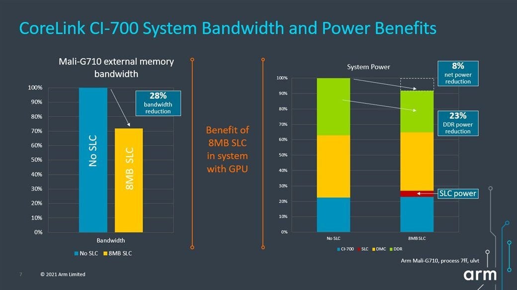
Like the L3 in current Intel chips, ARM’s system level cache (SLC) services both CPU and iGPU requests. They see a 28% hitrate from the iGPU side when using a 8 MB SLC, which is quite low. AMD similarly observed poor GPU Infinity Cache hitrates with cache sizes under 16 MB, from data published in their “Where Gaming Begins” presentation. Finally, I’ve gathered data using Intel’s Graphics Performance Analyzer (GPA) on a Haswell iGPU. While metrics are hard to interpret, they certainly don’t suggest great hitrates no matter how you look at them.

Low hitrate means you really have to think hard about whether an extra layer of cache is worth it. iGPU memory accesses are going through the L3 controller for a lookup, but more often than not end up going to DRAM anyway. Then, data fetched from DRAM to satisfy misses gets filled into L3 along with being forwarded to the iGPU. If not carefully managed, you could get capacity and bandwidth contention with CPU-side L3 accesses.

Intel has also been equipping their iGPUs with larger private caches, which makes the iGPU less dependent on the shared L3. Newer Xe parts have larger private caches than AMD’s Vega and RDNA 2 iGPUs, and actually come close to some midrange discrete GPUs in terms of cache capacity. For example, Nvidia’s RTX 3060 has 3 MB of L2 cache. If this trend continues, Meteor Lake’s iGPU should have enough cache to stand on its own without leaning on the CPU’s L3. After all, AMD’s Renoir and Cezanne have provided competitive iGPU performance with just a 1 MB L2 and no ability to share the CPU’s L3 with the iGPU.
Zooming Back Up
While Meteor Lake physically looks like a very tightly integrated design, I think it’s better to see it a variation of AMD’s chiplet strategy, but with more disaggregation and with reach traded for power efficiency. Meteor Lake is not Sapphire Rapids, where high bandwidth, low latency die-to-die connection are used to run the L3’s mesh interconnect across dies.

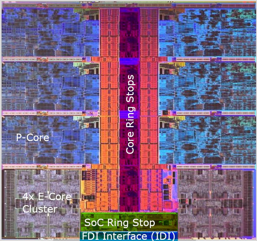
Instead, Meteor Lake’s FDI links likely have similar performance characteristics to AMD’s IFOP links, just with lower power. They’re therefore not used in any performance critical paths. The SoC to IOE link handles DisplayPort and PCIe traffic, which is much higher latency and lower bandwidth than DRAM traffic. Most iGPU memory accesses should be caught by the iGPU’s private cache, so the iGPU to SoC link is handling (hopefully infrequent) GPU cache miss requests. Similarly, the CPU’s L3 should catch most memory accesses coming from the cores, which should keep CPU to SoC traffic low too. The SoC probably has a ring stop on the CPU tile, which ensures the cross-die link only sees IDI packets addressed to the SoC, and keeps “hotter” traffic passing through the ring stop within the CPU tile. Notice the CPU tile is oriented with the E-Cores closest to the SoC tile, and has quite a bit of logic between the E-Core ring stops and the die edge. If I had to guess, there’s quite a bit of queuing and arbitration logic for requests to the SoC tile located on the CPU tile.
To take guessing even further, I think Meteor Lake may improve Intel’s L3 performance. The L3’s ring bus is completely contained within the die, and only has enough stops to handle L3 functionality for the cores. That makes it a lot like Zen 3.
Putting it Together
Going forward, Meteor Lake’s tile strategy should provide Intel with both cost savings and better modularity. Compared to AMD, Intel will be able to employ chiplets in mobile market segments, where tight power constraints prevent AMD from using their more power hungry IFOP links.
However, AMD’s Dragon Range lineup of CPUs designed for the high performance mobile market (55+ watts) is rumored to be using the same chiplet architecture as AMD’s Desktop CPUs. AMD also said in their Analysis Day Press Release that Phoenix Point – which AMD is putting in the 15 to 45 watt range – will also be using a chiplet architecture. This move to chiplets for even 15 watt TDP CPUs suggests that AMD may have a new potential chiplet implementation that could be more similar to Intel’s Meteor Lake. Without any more details beyond the presence of “AMD chiplet architecture”, I think it’s fair to say that it’s within the realm of possibility and regardless we’ll be excited to see how AMD implements chiplets on low power mobile chips.
Intel also disaggregates their design more than AMD’s, with separate iGPU and IO extender tiles. AMD packs those into their IO die. Intel thus has more tile reuse potential, though of course we’ll have to wait a few years to see how might they take advantage of that.
We’re looking forward to Meteor Lake’s launch, and thank Intel for a very interesting Hot Chips presentation.
If you like our articles and journalism and you want to support us in our endeavors then consider heading over to our Patreon or our PayPal if you want to toss a few bucks our way or if you would like to talk with the Chips and Cheese staff and the people behind the scenes then consider joining our Discord.
Sources
S. Naffziger et al, “AMD Chiplet Architecture for High-Performance Server and Desktop Products”, ISSCC 2020
K. Nasser et al, “Haswell: A Family of IA 22nm Processors”, IEEE 2014