
Hot Chips 34 – Tesla’s Dojo Microarchitecture

To say Tesla is merely interested in machine learning is an understatement. The electric car maker built an in-house supercomputer named Dojo, optimized for training its machine learning models. Unlike many other supercomputers, Dojo isn’t using off-the-shelf CPUs and GPUs, such as from AMD, Intel, or Nvidia. Instead, Tesla designed their own microarchitecture tailored to their needs, letting them make tradeoffs that more general architectures can’t make. In this article, we’re going to take a look at that architecture, based on Tesla’s presentations at Hot Chips. The architecture doesn’t have a separate name, so for simplicity, whenever we mention Dojo further down we’re talking about the architecture.
Block Diagram
At a high level, Dojo is an eight wide core with four way SMT, running at a conservative 2 GHz. It features a CPU-style pipeline, making it more tolerant of different algorithms and branchy code than something like a GPU. Dojo’s instruction set resembles RISC-V on the scalar side, but Tesla’s engineers have added a custom set of vector instructions focused on accelerating machine learning.

Tesla describes Dojo as a “high throughput, general purpose CPU”. There’s certainly some truth to that from a performance perspective. But to increase compute density, Tesla made sacrifices that would make Dojo cores extremely difficult to use compared to the CPUs we’re familiar with in our desktops, laptops, and smartphones. In some ways, a Dojo core handles more like an SPE in IBM’s Cell than a conventional general purpose CPU core.
Like a Cell SPE?
In the mid 2000s, IBM’s Cell processor featured eight “Synergistic Processing Elements”, or SPEs, controlled by a fully featured CPU core (“Power Processing Element”, or PPE). At first glance, Dojo shares a lot of similarities with the SPEs. Both Dojo and SPEs are optimized for vector processing, and rely on separate host processors for work assignment. Code running on Dojo or an SPE cannot directly access system memory. Instead, applications are expected to work mainly out of a small pool of local SRAM. This local SRAM is managed by software, and doesn’t work as a cache. If data from main memory is needed, it has to be brought in using DMA operations. Finally, Dojo and Cell’s SPEs both lack virtual memory support. We’ll go more into what that means later, but in short, it makes multitasking very difficult.
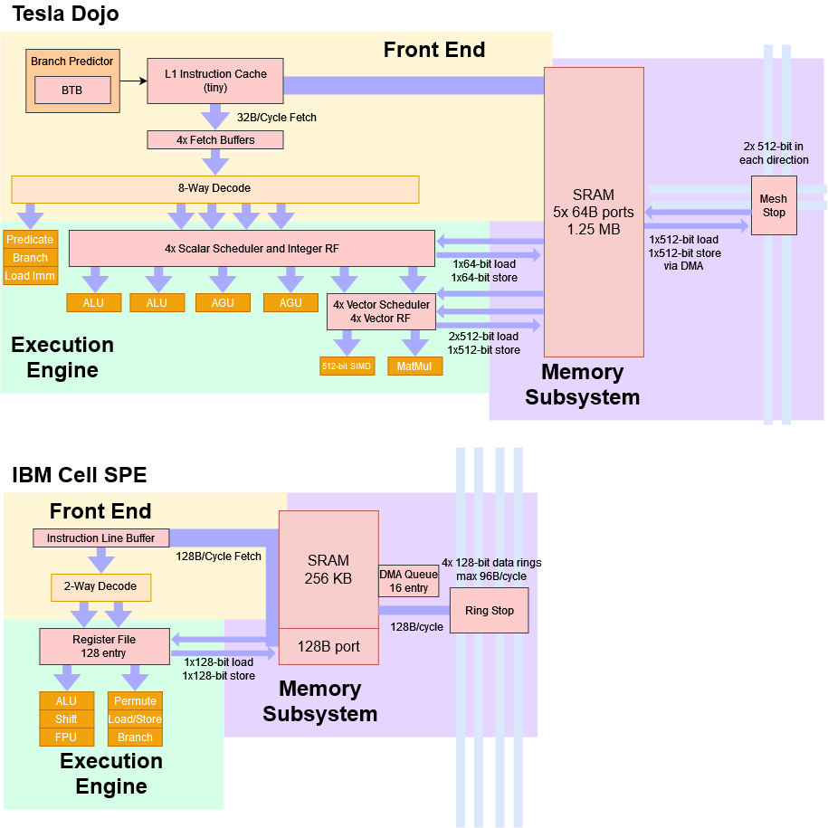
Dojo is different in several important ways. Since Dojo is not designed with small-scale deployments in mind, the host processors reside on separate host systems. These host systems have PCIe cards with interface processors, which then connect to Dojo chips over a high-speed network link. In contrast, Cell’s host processor resides on the same die. That makes it possible to deploy a single Cell chip by itself – something not possible with Dojo. Dojo’s 1.25 MB local block is SRAM is much larger and has higher bandwidth than a Cell SPE, which only has 256 KB of SRAM. Cell’s 256 KB SRAM only has a single port capable of delivering 128B per cycle. Dojo’s SRAM has five 64B ports. And of course, architecture goals are very different. Dojo is wide and low clocked, while Cell SPEs feature narrow, deep pipelines designed for high clocks. But it’s funny that Cell’s high-level design concept is still relevant today.
Frontend: CPU Comforts and More
Let’s take a brief trip through Dojo’s pipeline, starting at the front end. There’s a branch predictor of some sort, as Tesla’s diagram shows a BTB (branch target buffer). Its prediction capabilities probably won’t approach what we see on AMD, ARM, and Intel’s high performance cores, as Dojo needs to prioritize spending die area on vector execution. But even a basic branch predictor is a huge step up from no predictor at all, and Dojo’s branch prediction capability should give it far better performance than a GPU when handling branchy code, or larger instruction footprints.
Once the branch predictor has generated the next instruction fetch pointers, Dojo can pull 32 bytes per cycle from a “small” instruction cache into per-thread fetch buffers. This instruction cache probably serves to reduce instruction bandwidth pressure on the local SRAM, making sure the data side can access the SRAM with as little contention as possible. Also, the instruction cache isn’t coherent. If new code is loaded into local SRAM, the instruction cache has to be flushed before branching to that new code.
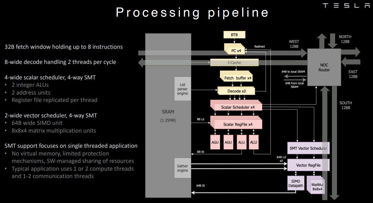
From the fetch buffers, Dojo’s decoder can handle eight instructions per cycle, from two threads. I’m a bit confused by what “two threads per cycle” means, since CPUs with SMT typically have fetch and decode handle one thread per cycle and switch between threads on cycle boundaries. Perhaps Dojo splits the decoder into two clusters and selects two threads to feed them every cycle. That may reduce decode throughput loss from taken branches.
At decode, certain instructions like branches, predicated operations, and immediate loads (“list parsing”) can be executed within the front end and dropped from the pipeline. It’s a bit like newer x86 CPUs eliminating register-to-register copies in the renamer. But you heard that right – Dojo is not tracking “eliminated” instructions through the pipeline to maintain in-order retirement. Other processors track everything to retirement so that they can stop at any instruction boundary, and maintain all the state necessary to resume execution. This capability is called “precise exceptions”, and is used by modern operating systems to deliver all kinds of goodies like paging to disk, or telling you exactly where you screwed up in your code.
Tesla does not care about delivering precise exceptions. Dojo does feature a debug mode where more instructions go through the pipeline to give “more precise” exceptions, but there is no in-order retirement logic like on normal out-of-order CPUs.
Dojo’s Execution Engine
After seeing a wide front end, it might be a bit weird to see a 4-wide integer execution engine with just two ALUs and two AGUs. But this funnel-shaped pipeline makes sense because some instructions are executed and dropped within the front end. Dojo also isn’t going into client systems, where scalar integer performance is important. So, the integer side provides just enough throughput to crunch through control flow and address generation in order to keep the vector and matrix units fed.
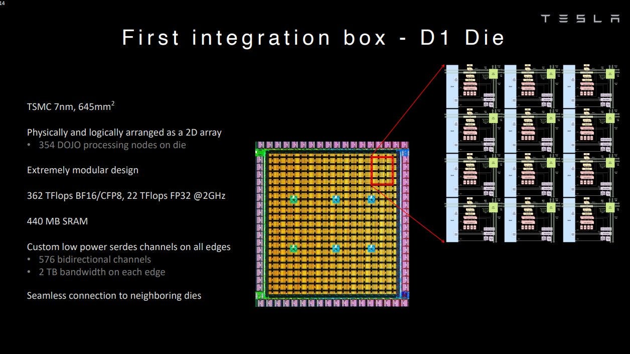
Dojo’s vector and matrix execution side is placed after the scalar execution engine in the core’s pipeline and has two execution pipes. Two pipes might not sound like much, but Dojo has very wide execution units behind those pipes. One pipe can do 512-bit vector execution, while the other does 8x8x4 matrix multiplication. So, Dojo is capable of very high throughput as long as instructions expose enough explicit parallelism – especially if the matrix unit is used. Tesla claims a die with 354 Dojo cores can hit 362 BF16 TFLOPS at 2 GHz, indicating that each core can do 512 BF16 FLOPS per cycle.
We’re not sure whether Dojo can do full out-of-order execution. But Tesla did say the integer side could run very far ahead of the vector side, suggesting that it can execute past stalled instructions until one of the schedulers fills. Lack of in-order retirement also points to out-of-order execution capability.
Normally, implementing out-of-order execution introduces a lot of complexity. That’s because the CPU has to appear to execute instructions in-order. AMD, ARM, and Intel’s high-performance CPUs track instructions with large reorder buffers (and other structures) so that their results can be committed in program order. That means if a program does something stupid like divide by zero, those cores can show exactly which instruction was at fault. And, they can show CPU state that reflects actions from all instructions before the faulting one, but none after. That means you can fix whatever made the instruction fault, and resume execution. Dojo gives up this capability. In exchange, Dojo can avoid the power and area overhead associated with tracking every instruction through its pipeline to make sure results are committed in program order.
SRAM Access
Normally, we would talk about caching here. But Dojo cannot directly access system memory, so we’ll talk about that 1.25 MB block of SRAM. It can handle two 512-bit loads per cycle, making its per-cycle bandwidth a match for Intel’s CPUs with AVX-512 support. Tesla says the SRAM has five 512-bit ports (2x load, 1x store, and two to the mesh stop). But the scalar side only has two AGUs, which likely means the core can’t sustain two 512-bit loads and a 512-bit store every cycle.
Because Dojo’s local block of SRAM is not a cache, it doesn’t need tags and state bits stored alongside the data. There’s also no L1D cache in front of the SRAM, so it has to be fast enough to handle all load and store instructions without causing bottlenecks, even though its size is closer to that of a L2 cache. Not implementing the SRAM as cache is probably how Tesla keeps latency low. If we look back at AMD’s Hammer architecture from long ago, we can see that accessing the 1 MB L2 takes eight cycles after an L1D miss is detected (for 12 cycles of total latency). Three stages can probably be dropped if that 1 MB of SRAM was directly addressed instead of being used as a cache, bringing latency down to 5 cycles:

Factor in a couple decades worth of process node improvements and even lower clock speed targets than Athlon’s, and it’s easy to see how Tesla could access a L2-sized block of SRAM with L1-like latency. Skipping a level of cache of course saves area and power.
To further cut down on latency, area and core complexity, Dojo has no virtual memory support. So, it has no TLBs or page walk mechanisms. Modern operating systems take advantage of virtual memory to give each process its own view of memory. Instead of directly accessing physical memory addresses, memory addresses used by the program are translated by the CPU to physical addresses, using paging structures set up by the operating system. That’s how modern operating systems keep programs isolated from each other, and prevent one misbehaving application from bringing down the entire system.
Virtual memory is also how you can run more programs than you have physical memory for. When you run out of real memory, the operating system unmaps a page, writes it to disk, and gives your program the memory it asked for. When that other poor program tries to access that memory, the CPU tries to translate the virtual address to a physical one, but finds that the translation isn’t present. The CPU throws a page fault exception, which the OS handles by reading the evicted page back into physical memory and filling out the page table entry.
None of that is doable on Dojo. The core’s 4-way SMT capability is more for a single application to expose explicit parallelism, instead of boosting multi-tasking performance. For example, one thread could perform vector compute, while another asynchronously loads data from system memory into SRAM (via DMA).
To further simplify the design, Dojo could address the SRAM with only 21 address bits, which could simplify Dojo’s AGUs and addressing buses. These tradeoffs probably let Tesla access that SRAM with low enough latency to avoid implementing a separate L1 data cache in front of it.
DRAM Access
Speaking of system memory, Dojo chips don’t directly connect to memory. Instead, they connect to interface processors, which are equipped with HBM. These interface processors are also responsible for communicating with host systems.
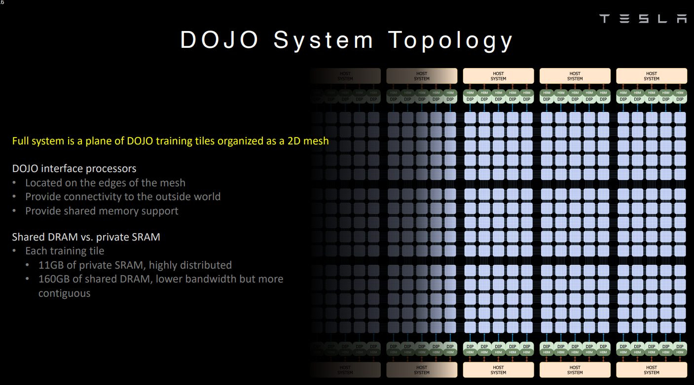
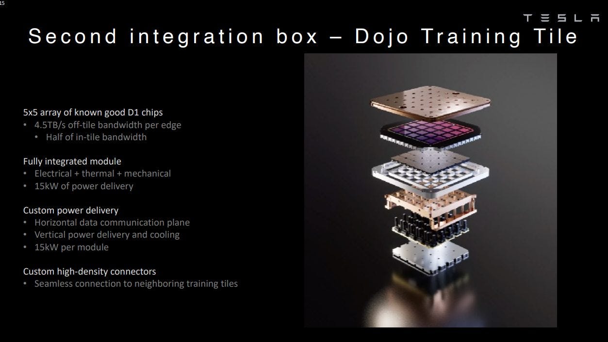
A Dojo tile with 25 individual chips has access to 160 GB of HBM memory. Tesla says they can transfer 900 GB/s out of each die edge across tile boundaries, which means the interface processors and their HBM can be accessed with 4.5 TB/s of link bandwidth. Because accessing HBM involves going through a separate chip, access latency is likely very high.
It’s Tiny. How?
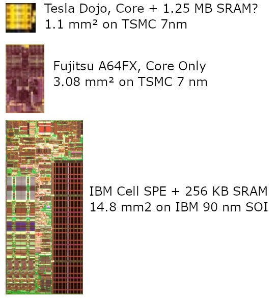
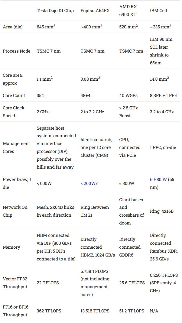
Dojo is an 8-wide core with at least some OoO execution capability, decent vector throughput, and a matrix multiplication unit. But even with 1.25 MB of local SRAM, it ends up being a very small core. For comparison, Fujitsu’s A64FX occupies more than twice the area on the same process node.
Processor design is all about making the right tradeoffs. Tesla wants to maximize throughput for machine learning by packing tons of cores onto the die, so individual cores have to be small. To achieve its area efficiency, Dojo uses some familiar techniques. It runs at a conservative 2 GHz. Lower clocking circuits tend to take less area. It probably has a basic branch predictor, and a small instruction cache. That sacrifices some performance if programs have a large code footprint or lots of branches.
But Tesla also goes a lot further to minimize power and area usage by chopping features that aren’t necessary for running internal workloads. They don’t do data-side caching, don’t support virtual memory, and don’t support precise exceptions.
The result is a processor core that delivers the performance flexibility of a modern CPU core, while in many ways being less user and programmer friendly than an Intel 8086. Beyond the core, Tesla also saves die area by designing Dojo chips specifically for deployment at a large scale.
Physical Implementation
Zooming out, Dojo cores are implemented on a very large 645 mm2 die, called D1. Unlike other chips we’re familiar with, a single Dojo die isn’t self-sufficient. It doesn’t have DDR or PCIe controllers. There are IO interfaces around the die edge, which let the die communicate with neighboring dies, with a latency of about 100 ns.
To get to system memory, a Dojo D1 die has to communicate with an interface processor, which has onboard HBM. That interface processor is in turn connected to host systems via PCIe (the interface processors are mounted on PCIe cards). Theoretically, the smallest functional Dojo deployment would involve a Dojo die, an interface processor card, and a host system. But Tesla deploys Dojo dies in modules containing 25 dies each, to give a sense of scale. Dojo D1 dies are designed specifically to be building blocks for a supercomputer, and nothing else.
This specialization allows more die area savings. Dojo D1 doesn’t spend area on DDR and PCIe controllers. Most of the die is occupied by a sea of Dojo cores, except for custom IO connectors around the outside designed to interface with neighboring dies.
In comparison, chips designed with more deployment flexibility in mind spend a ton of area on IO. AMD’s Zen 1 “Zeppelin” die is a great showcase of this. Zeppelin can directly connect to DDR4 memory, PCIe devices, SATA drives, and USB devices – perfect for meeting client requirements. In servers, IFOP interfaces let it communicate with neighboring dies. Large blocks of SRAM positioned near IFOPs are likely snoop filters that help efficiently maintain cache coherency across high core count setups. Dojo doesn’t try to maintain cache coherency across cores, and doesn’t use any SRAM for snoop filters.
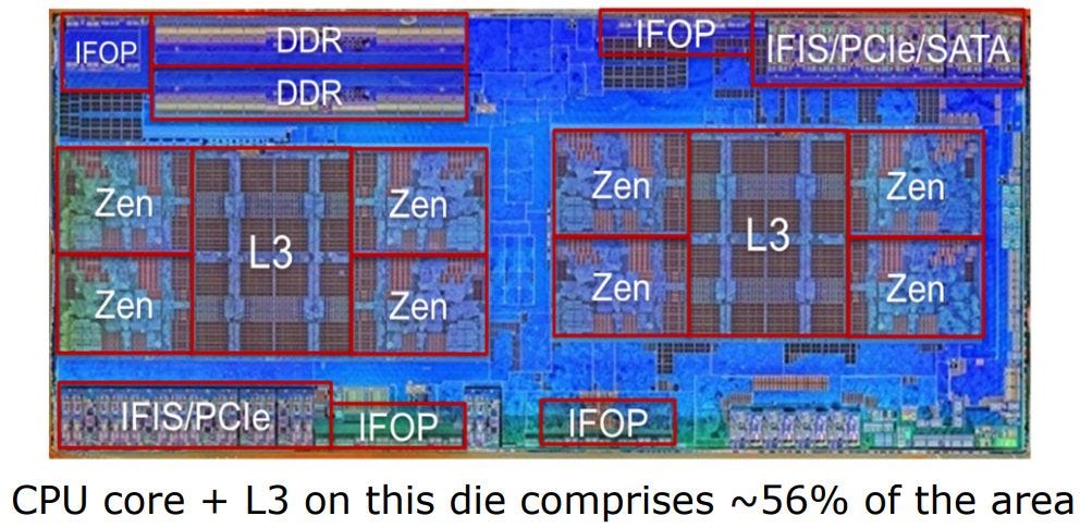
AMD pays for this flexibility by spending about 44% of “Zeppelin” die area on logic other than cores and cache. Dojo only spends 28.9% of die area on things other than SRAM and cores.
Final Words
The microarchitecture behind Tesla’s Dojo supercomputer shows how it’s possible to achieve very high compute density, while still maintaining a CPU’s ability to perform well with branchy code. To get there, you give up most of the comforts that define our modern computing experience. If you could hypothetically build your desktop around a Dojo core, the experience would probably feel familiar to anyone who has used MS-DOS. You can’t run several applications simultaneously. A single misbehaving application can force you to reboot the system. If you don’t have enough RAM to run a certain program, you can forget about running it at all (no paging to disk).
But these tradeoffs make perfect sense in Tesla’s supercomputer. Tesla doesn’t need Dojo cores to handle several running applications at once, and Dojo only has to run internal, trusted code. So, Tesla doesn’t care about virtual memory support. Similarly, machine learning programs running on Dojo will be written with that specific system in mind. You won’t have a batch of arbitrary programs possibly asking for more memory than is available. That means you don’t need precise exceptions (and virtual memory) to allow techniques like overcommitting memory, memory compression, or swapping memory pages to and from disk. Precise exceptions are also useful for debugging, but Tesla makes debugging possible in a cheaper way with a separate debug mode. That way, after the code has been written and debugged, Dojo can focus on running it without doing the bookkeeping necessary to commit instruction results in-order.
For sure, the tradeoffs employed by Tesla to get high compute density aren’t possible in a consumer or server CPU. But they’re very interesting to see in action, and we have to thank Tesla for taking the time to present at Hot Chips. For the past two decades, process node improvements have been slowing down, resulting in slower advances in single-threaded performance. For the past half-decade, power supply and cooling limitations have been slowing down multithreaded performance. But the appetite for more computing power is not slowing down, so companies are turning to more specialized hardware to keep pace. The architecture in Tesla’s Dojo supercomputer is an excellent example of how tradeoffs can be made to increase compute density, and how current trends favor introducing specialized hardware for throughput bound applications.
If you like our articles and journalism and you want to support us in our endeavors then consider heading over to our Patreon or our PayPal if you want to toss a few bucks our way or if you would like to talk with the Chips and Cheese staff and the people behind the scenes then consider joining our Discord.
Interesting blog post. Is the Dojo hardware code or its simulation open-sourced?