
Alder Lake’s Caching and Power Efficiency

Processor caches are known to improve performance, but they also significantly influence power efficiency. Modern CPUs spend a lot of power to move data around. If data can be pulled from sources closer to the core, the CPU can spend less power moving data. This article will examine data transfer energy costs on Intel’s Alder Lake, by using a modified version of our memory bandwidth benchmarks that reads package power counters. Specifically, the package power counter MSR (0x611 on Intel, 0xC001029B on AMD) is read before and after the test for each data point. We then convert the difference into joules using the units given by the respective power unit registers, and derive data from there.
For perspective, we’ll be comparing Golden Cove cores with previous generations of Intel big cores, namely Haswell and Skylake. For Gracemont, we’ll bring in some data from Tremont and Goldmont Plus, since those are previous iterations in Intel’s Atom line. AMD’s Zen 2 and 3 will be included too, though that data should be taken with a grain of salt since AMD’s sensors appear to model power instead of directly measuring it.
All tests here were run with four cores active, because some of the CPUs tested here only have four cores. Each thread gets a separate array, which means we’ll be seeing the sum of private cache capacity. In other words, if each of the four cores have a 32 KB L1D, we’ll spill out of that as test size exceeds 4 * 32 = 128 KB.
Golden Cove
In Alder Lake’s hybrid core setup, Golden Cove cores target maximum performance. A Golden Cove core has a three-level cache hierarchy, with a 48 KB L1D, 1280 KB L2, and a 30 MB L3 shared across all cores (and the iGPU). Predictably, pulling data from each successive level in the memory hierarchy costs more power than the previous one.

Pulling data from DRAM costs a staggering amount of power compared to hitting cache, at almost 5X as much power per bit compared to getting data from L3. Actual DRAM power cost is even higher than our data would suggest, since we’re only looking at package power, without factoring in DRAM power. Another note is that we’re using DDR4-3200 in this test due to DDR5 board issues. Titanic from our team does not want to deal with that setup anymore.
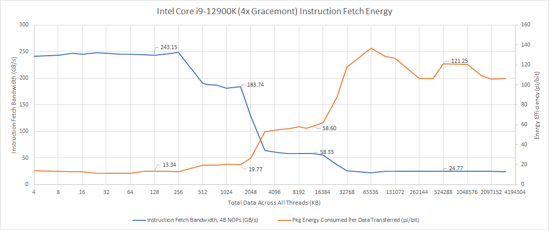
The instruction side shows the same pattern, though energy costs are a bit higher overall because data is moved in smaller chunks. While AVX instructions can load data 256 bits at a time, we’re using 32-bit (4 byte) NOPs to measure instruction bandwidth. Interestingly, there’s very little power overhead to using the L1 instruction cache and fetch/decode path instead of the micro-op cache.

Since each instruction here is 4 bytes, micro-op cache capacity would be 4 bytes * 4K ops * 4 cores = 64 KB. After that point, power per instruction fetched only increases by 6.5%. For comparison, we see a staggering 77% increase in power per instruction when we hit L2. Perhaps a micro-op cache isn’t so sensible for low power designs. The SRAM used to implement a micro-op cache would be better spent preventing instruction fetches from going to L2. And that’s exactly Gracemont’s strategy.
Gracemont
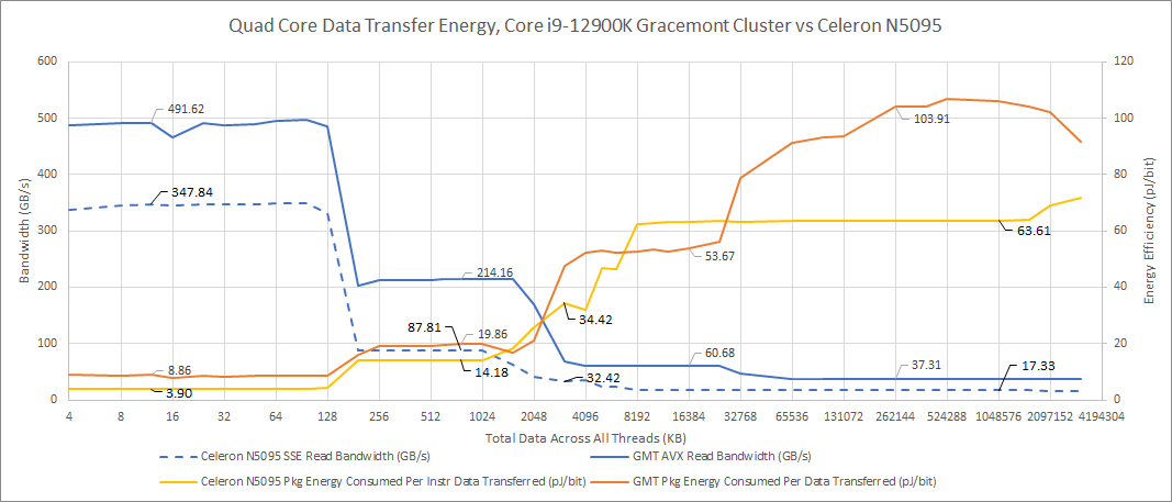
While Golden Cove targets maximum performance, Gracemont aims to balance performance with area and power efficiency. It also has a three level cache hierarchy, but the L2 is larger at 2 MB, and shared by a quad core cluster. Curiously, Gracemont doesn’t score an overall power efficiency win over Golden Cove. DRAM access is more efficient, but power cost to hit cache is higher.

Gracemont’s worse efficiency in L1D could be because the core is moving data at smaller granularities. Even though it supports AVX, 256-bit ops are split into two 128-bit ops. That means the core largely doesn’t benefit from AVX’s 256-bit vector length. At L2, Gracemont’s larger, shared cache is more complex than a core-private one. The design likely trades bandwidth and power efficiency for lower area cost. While Gracemont draws less power, it ends up consuming more energy to move the same amount data out of its L2 because the core has to stay powered up for longer.
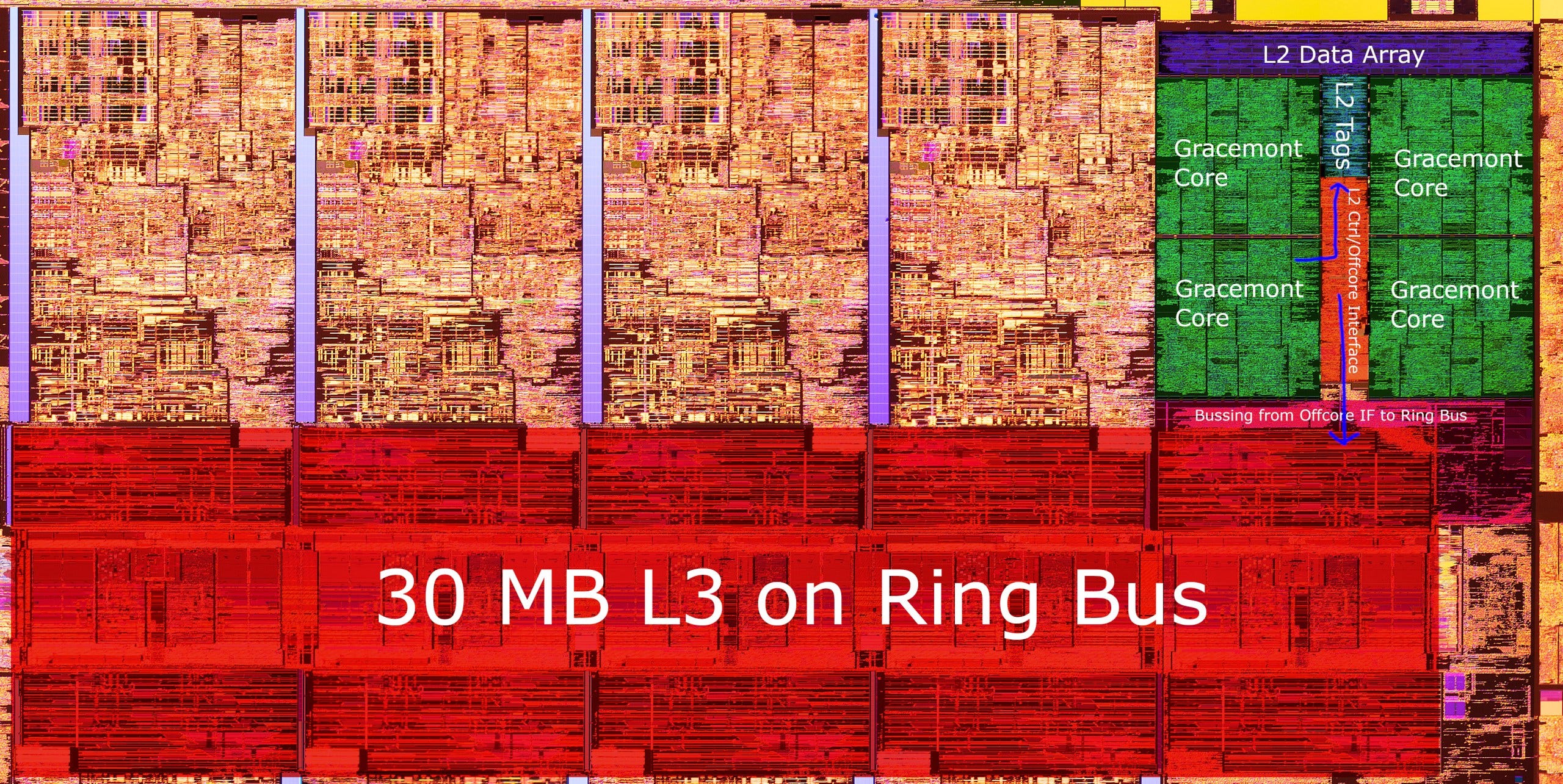
Gracemont’s shared L2 controller and offcore interface is probably also a complex piece of logic that draws a good chunk of power by itself. Labeled in orange above, this block is responsible for handling L2 requests coming from all cores in the cluster, and arbitrating between them. That means each Gracemont core has a less direct path to the ring bus. That’s probably what gives Golden Cove an energy efficiency win when hitting L3.
When we get to DRAM, Gracemont wins because the smaller out-of-order execution engine burns less power while being bottlenecked by memory.
The situation changes a bit from the instruction side. Gracemont’s L1i fetch and decode path is slightly more power efficient than Golden Cove’s, but not a match for Golden Cove’s micro-op cache. We’re really splitting hairs about that though – differences are well under 10% either way. When instructions have to be fetched from L2, Gracemont pulls a slight win over Golden Cove. At L3 and DRAM test sizes, we mostly see a repeat of the data-side situation.
Golden Cove vs. Older Intel Big Cores
Compared to Skylake, Golden Cove’s L1D has roughly the same efficiency while achieving far higher bandwidth. Intel has impressively managed to implement extra load ports and run at higher clock speeds, without losing power efficiency. That speaks to how well Intel evolved their 10nm process into Intel 7.

Golden Cove’s L2 is also impressive, achieving slightly better energy efficiency while providing more capacity and higher bandwidth than Skylake’s L2. The L3 situation is more mixed – Skylake’s smaller ring and lower L3 capacity mean L3 reads cost less energy than on Golden Cove. But Golden Cove’s larger L3 should mean fewer expensive DRAM accesses. Out in DRAM, first-generation Skylake has a slight efficiency edge, since it’s not running massive core structures at high clock speeds while bottlenecked on DRAM.

Against Haswell, it’s a massacre. For an architecture that’s almost ten years old, Haswell can move data pretty fast, but Intel’s 22nm process is no match for the newer process nodes; as a result, Haswell is less energy efficient at every cache level. Haswell’s DDR3 memory is also very inefficient compared to the DDR4 setups used by newer platforms.
On the instruction side, Golden Cove mostly compares favorably to Skylake. The L2 cache is an exception. Somehow, Skylake has a very power efficient instruction fetch path to L2. Like Golden Cove, Skylake loses very little power efficiency when it misses the micro-op cache and has to fetch and decode instructions from the L1i.
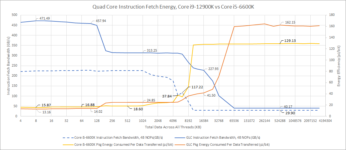
Once again, Haswell is no match for Golden Cove, due to its much older process node. Strangely, it doesn’t seem to gain any power efficiency from using the micro-op cache (or gains were within margin of error).

Overall, Golden Cove’s newer process and architecture give it an edge in power efficiency when it comes to moving lots of data. Across three different generations of Intel big cores and three process nodes, we see the same general pattern of increasing power costs as each level of cache is missed. This pattern underscores how important caching is to power efficiency. Now, let’s look at AMD.
Compared to AMD
The picture with AMD is remarkably similar. While there are caveats with using AMD power data, as we mentioned into the introduction, AMD doesn’t seem to hold an efficiency advantage for core-private caches. Power efficiency figures for L1 and L2 are remarkably close for Zen 2 and Golden Cove. AMD does hold an edge when we get to L3, likely because the on-chip network that connects Zen 2 cores to L3 only handles four cores and their respective L3 slices. In contrast, Golden Cove’s ring bus has to connect ten L3 slices and just as many cores or core clusters.
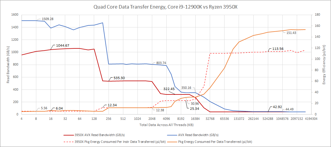
In DRAM, AMD’s power efficiency resembles Skylake’s. One funny observation is that Skylake and Zen 2 have roughly similar out-of-order engine sizes. Again, I suspect Golden Cove is wasting a lot of power running its very large out-of-order engine at high clocks while bottlenecked on memory.
The instruction side is slightly different. Golden Cove has a slight edge when fetching instructions from the micro-op cache. Unlike Intel’s architectures, Zen 2 suffers a notable increase in power per instruction fetched when it misses the micro-op cache, and has to bring instructions in through the L1i fetch/decode path.

Zen 2 however enjoys better power efficiency if instructions fetches miss L1i, but come from lower cache levels. And in DRAM, AMD loses the power efficiency lead it enjoyed on the data side.
Zen 3 regresses in power efficiency, and takes more power to pull the same amount of data out of its core private caches. However, it still pulls a win in L3 sized regions. AMD’s excellent L3 design lets Zen 3 get higher bandwidth out of its L3 cache with slightly lower power cost.

Compared to Zen 2, Zen 3 likely requires more power because its stock boost clocks are much higher. On top of that, the Zen 3 system is running faster memory. That means higher infinity fabric clock, and more power draw from the IO die. The situation repeats on the instruction side, except Zen 3 loses its power efficiency advantage in L3 regions.

Intel has very strong core-private caches, while AMD has a very strong L3 cache. Overall there’s not a huge difference between Intel and AMD in terms of data transfer power efficiency. If AMD has a significant power efficiency advantage, it’s likely due to core differences and the ability to use smaller OoO structures to achieve similar performance. AMD’s lower cache latency plays a role in that, letting the core go further with less reordering depth.
Finally, keep in mind that AMD’s RAPL counters are likely modeled, not measured, and won’t be as accurate as Intel’s. So take the metrics in AMD’s section with a grain of salt – they’re probably a reflection of how much power AMD thinks their processors are drawing.
Atom’s Progression
Now, let’s look at how Gracemont compares to its ancestors. We’ll start with Tremont – Gracemont’s direct predecessor. It’s implemented on Intel’s 10 nm process, and is a smaller core that targets lower clocks. Like Gracemont, Tremont uses a triple-level caching hierarchy. Each core has a private 32 KB L1D, while a cluster of four cores share a 1.5 MB L2 and 4 MB L3.
With a power efficient design at sub-3 GHz clocks, Intel’s 10nm process node sips power. At every level in the cache hierarchy, Tremont draws less power per bit transferred than Gracemont. In DRAM, Tremont is so efficient that I wonder how accurate the RAPL counters are. According to those counters, the whole package drew just 9.5 W when running the memory bandwidth test with DRAM-sized regions. The i9-12900K drew around 30 W for comparison. I guess E-core efficiency gets overshadowed by Alder Lake’s large uncore power draw.
In return, Tremont is even more bandwidth constrained than Gracemont. Its L2 is small and low bandwidth; the same applies to Tremont’s L3. And Tremont lacks AVX support.
Gracemont’s efficiency is more comparable to that of Goldmont Plus. Goldmont Plus is Tremont’s predecessor – a 3-wide low power architecture implemented on Intel’s 14nm process. It has a simpler, two level cache hierarchy with a core-private 24 KB L1D, and a 4 MB L2 shared by all four cores.

Goldmont Plus’ caches end up being a hair more efficient than Gracemont’s, showing that Intel’s now outdated 14nm process can still be quite good at low clocks. Goldmont Plus’ 4 MB L2 is impressive, because pulling data from it costs less power than doing so from Gracemont’s smaller 2 MB L2. Perhaps that’s a reflection of how far Gracemont is pushed at stock in the i9-12900K. And maybe that’s why we don’t see low power designs from other manufacturers (like ARM) shoved to the upper 3 GHz range.
In terms of bandwidth though, Goldmont Plus is pretty horrible. Its low clocks and inability to execute multiple SSE loads per cycle mean bandwidth is even worse than Tremont’s.
From the instruction side, the story’s pretty similar. Again, Tremont is very efficient.

And again, Gracemont ends up in the same ballpark as Goldmont Plus. To Gracemont’s credit, its higher clock speed and wider pipeline give it more instruction throughput compared to the older 14nm Atom architecture.

But at the high frequencies Gracemont runs at, Intel’s 7 nm process doesn’t get to shine on the power efficiency front. Perhaps it’s best to look at Gracemont purely as an area efficient design, not one that focuses purely on power efficiency the way previous Atoms did.
Final Words
Over the past few years, increasing core counts and focus on multithreaded performance mean that power efficiency has become increasingly important. That apples even to desktops, which have traditionally emphasized performance over power efficiency. While there’s a lot of focus on how CPU cores are designed to maximize power efficiency, caching strategy also deserves attention.

Across all platforms we tested, we saw a consistent pattern where each level in the memory hierarchy cost more power to get data from than the previous level. As a rule of thumb, hitting L2 costs about twice as much power as hitting L1. Hitting L3 tends to cost more than twice as much power as hitting L2. Pulling data from memory is extremely expensive, with power costs typically 4-5x that of hitting L3.

Race to sleep logic also applies. Some of the CPUs we tested actually reported lower package power draw when testing DRAM-sized regions, compared to hitting cache. But DRAM bandwidth is so much lower than cache bandwidth that it ends up costing more energy over the time it takes to bring data in from DRAM. When cores are waiting for data, they need to keep their large out-of-order structures powered up. The more time they spend waiting for data, the more power they waste. This applies to slower cache levels as well, just to a lesser extent. That means keeping data close to the core is not just good for performance – it’s very important for power efficiency too. And we’re not the first ones to notice:
With Alder Lake, Intel has done a reasonably good job of using process node advancements to let Golden Cove deliver higher bandwidth at lower power consumption, compared to previous big cores. But Gracemont isn’t as impressive. Performance has improved for sure, but its efficiency when moving data around has regressed compared to Tremont.

Intel’s strategy seems to focus on reducing ring bus traffic by using large L2 caches. That’s partly because Intel’s longer ring bus and higher L3 slice count means L3 accesses tend to be more power hungry (and higher latency) than AMD’s. Intel’s excellent L2 design also plays a role. Golden Cove’s L2 is able to maintain very competitive data transfer power efficiency while offering more capacity and higher bandwidth than AMD’s. This is likely most beneficial with vector workloads that have high L1 and L2 hitrates.
AMD of course also wants to keep data as close to the core as possible. But it’s less critical on Zen 2 and Zen 3, since their L3 caches are superior to Intel’s in latency and power efficiency. AMD’s core-private caches are also less optimized for moving tons of data than Golden Cove’s. While Zen 2 and 3 are still strong performers for vectorized workloads, Intel’s latest big core architecture has a clear advantage in that area.
Going forward, we’re going to look closely at how each CPU maker adapts their caching strategy to keep performance high and power consumption low. We’ve already seen AMD increase L2 size on their upcoming Zen 4 architecture (from 512 KB to 1 MB). Rumors suggest Intel is doing the same on Raptor Lake as well, bringing L2 size from 1280 KB to 2 MB on P-Cores, and 2 MB to 4 MB on E-Core clusters.
If you like our articles and journalism and you want to support us in our endeavors then consider heading over to our Patreon or our PayPal if you want to toss a few bucks our way or if you would like to talk with the Chips and Cheese staff and the people behind the scenes then consider joining our Discord.