
Intel’s Netburst: Failure is a Foundation for Success

In the world of today’s high performance CPUs, major architectural changes don’t happen often. Iterating off a proven base is safer, cheaper, and faster than attempting to massively rework the basics of how a CPU fetches and executes instructions. But more than 20 years ago, things hadn’t settled down yet. Intel made two attempts to replace its solid but aging P6 microarchitecture with something completely different. One was Itanium, which avoided the complexity associated with out-of-order execution and variable length decode to deliver very wide in-order execution.
Pentium 4 was the other, and we’ll be taking a look at it in this article. Its microarchitecture, called Netburst, targeted very high clock speeds using a long pipeline. Alongside this key feature, it brought a wide range of innovative architectural features. As we all know, it didn’t quite pan out the way Intel would have liked. But this architecture was an important learning experience for Intel, and was arguably key to the company’s later success.
This article will mostly focus on the late variants of the Netburst architecture, implemented on the 90 nm (“Prescott”) and 65 nm (“Cedar Mill”) process nodes with 64-bit support. As another note, we understand this look into Netburst comes slightly late. The last of the Netburst architecture chips were discontinued 13 years ago, so this article may not necessarily fit the definition of a launch date review. To compensate for that, we’ll use period-correct graphs, created on Office XP….running on Windows 11. Enjoy.
Block Diagram and Overview
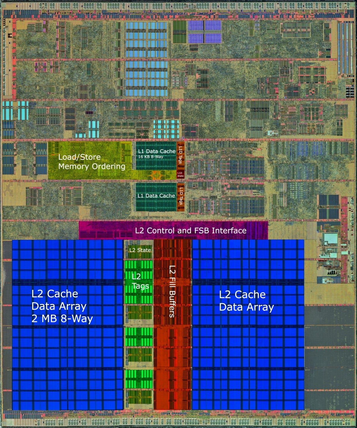
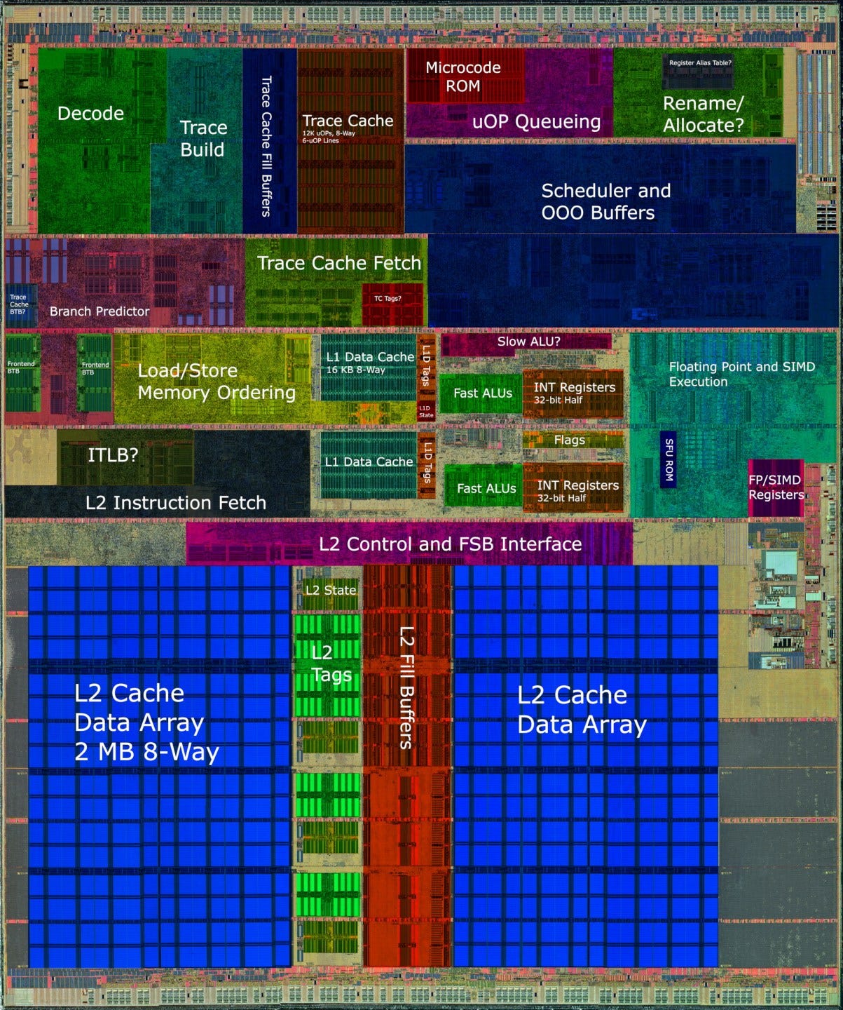
For its time, the Netburst architecture was a massive core. Next to its predecessor, the Pentium III, the Pentium 4 has more execution resources and much larger out of order structures. It’s also a large core compared to AMD’s competing Athlon 64, and even it’s successor, Merom.

Compared to the Pentium III, based off Intel’s P6 architecture, Netburst is on a completely different scale. While both have pipelines that are three-wide, every key out of order structure on Netburst is several times larger.

Frontend: Branch Prediction
Branch prediction is extremely important for any CPU, and that especially applies to the Pentium 4. It needs very good branch prediction accuracy to take advantage of its huge (for the time) reordering capacity. On top of that, Netburst’s relatively long pipeline needs a lot of cycles to detect a mispredicted branch.
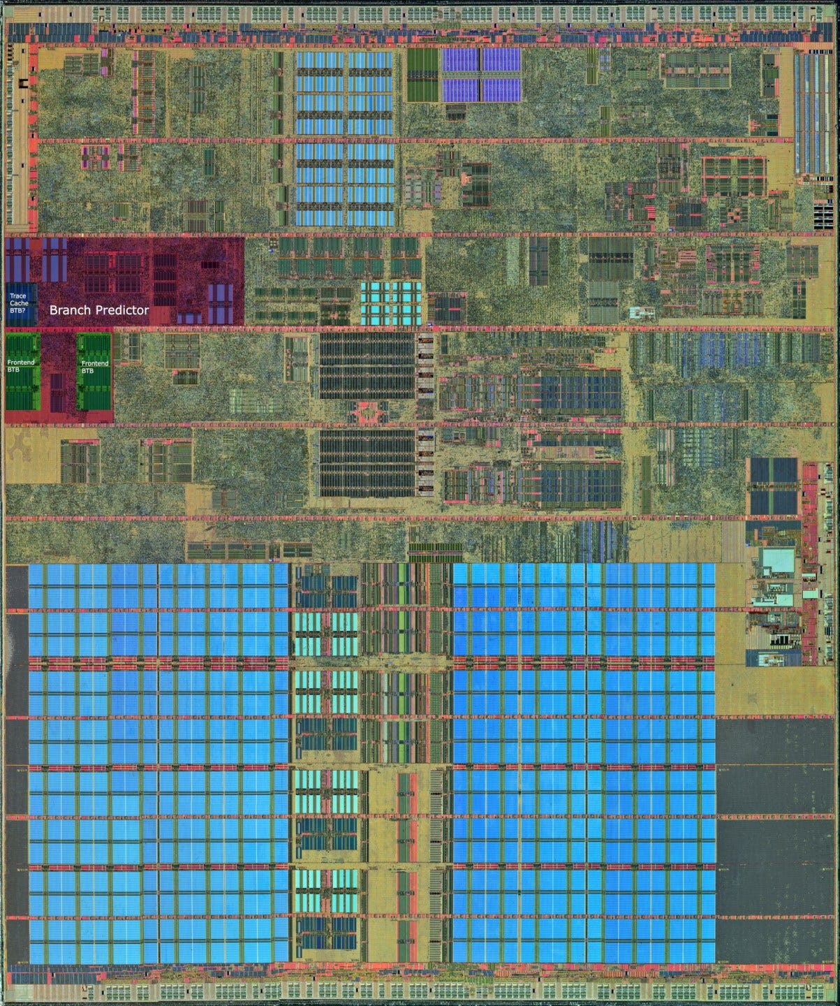
According to Agner Fog, the Pentium 4 uses a two-level adaptive predictor with a 16-bit global history buffer. In our testing, the Pentium Extreme Edition 965 seemed able to recognize a 24-long repeating pattern, so it’s possible this capability was expanded in Netburst’s 65nm revision. In any case, this branch prediction capability is very advanced for the time, and even exceeds that of its successor, Merom (also known as Core 2). There’s no doubt that the branch predictor was very high up on Intel’s priority list, in terms of both engineering effort and die area allocation.


To speed up taken branch handling, Intel has implemented very large branch target buffers. Combined with the trace cache, which we’ll discuss in more detail below, this provides tremendous zero-bubble taken branch capability. Netburst can track over 1024 branches and handle them without needing the frontend to stall while a branch target is looked up. If code is very branch-dense, this figure can exceed 2048 branches. Intel chips didn’t provide comparable zero-bubble capability until Gracemont in 2021, and AMD didn’t either until Zen 3 launched in 2020.
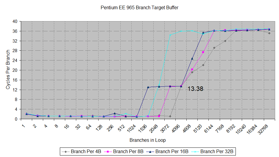
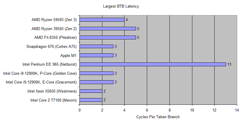
But once Netburst’s zero-bubble tracking ability is exceeded, branch handling speed takes a nose dive. The architecture is probably using its 4096 entry BTB, and that path is extremely slow. We see over 13 cycles (12 pipeline bubbles) incurred for every taken branch. This is similar to what is referred to as a BTB miss penalties in other CPUs.
Finally, after what looks like a BTB miss, taken branch latency goes through the roof, hitting an incredible 36 cycles per branch. This extreme penalty is likely why the CPU needs such a large 4096 entry main BTB. At this point, Netburst is probably fetching instructions from L2 and using a branch address calculator to resolve targets.

Merom and Westmere, which succeeded Netburst, cannot achieve the same speed for small branch footprints. After four or eight branches respectively, Merom and Westmere suffer a 1 cycle bubble after a taken branch. When their BTB capacity is exceeded, both newer CPUs can actually handle taken branches faster than Netburst can using its large 4096 entry BTB.
Frontend: Fetch and Decode
Netburst uses a radically different approach to instruction caching – one that hasn’t been seen before or repeated in mainstream processors. It replaces the traditional L1 instruction cache with a 12K entry trace cache. Instead of storing instruction bytes, this trace cache stores micro-ops corresponding to decoded instructions. And instead of having a simple one-to-many relationship between cache lines and cacheable memory addresses, the trace cache stores traces of sequentially executed instructions. Thus a single instruction can be cached in several places within the trace cache if it’s the target of several different branches. This is done to improve frontend bandwidth by turning taken branches into not-taken ones, from the instruction fetch logic’s perspective.
This is important because a micro-op cache or traditional L1i fetch and decode setup tends to lose a lot of frontend bandwidth around taken branches. Fetch or decode width that goes past a taken branch becomes useless, and getting the taken branch target requires a separate fetch request. Netburst’s trace cache tries to get rid of these penalties.
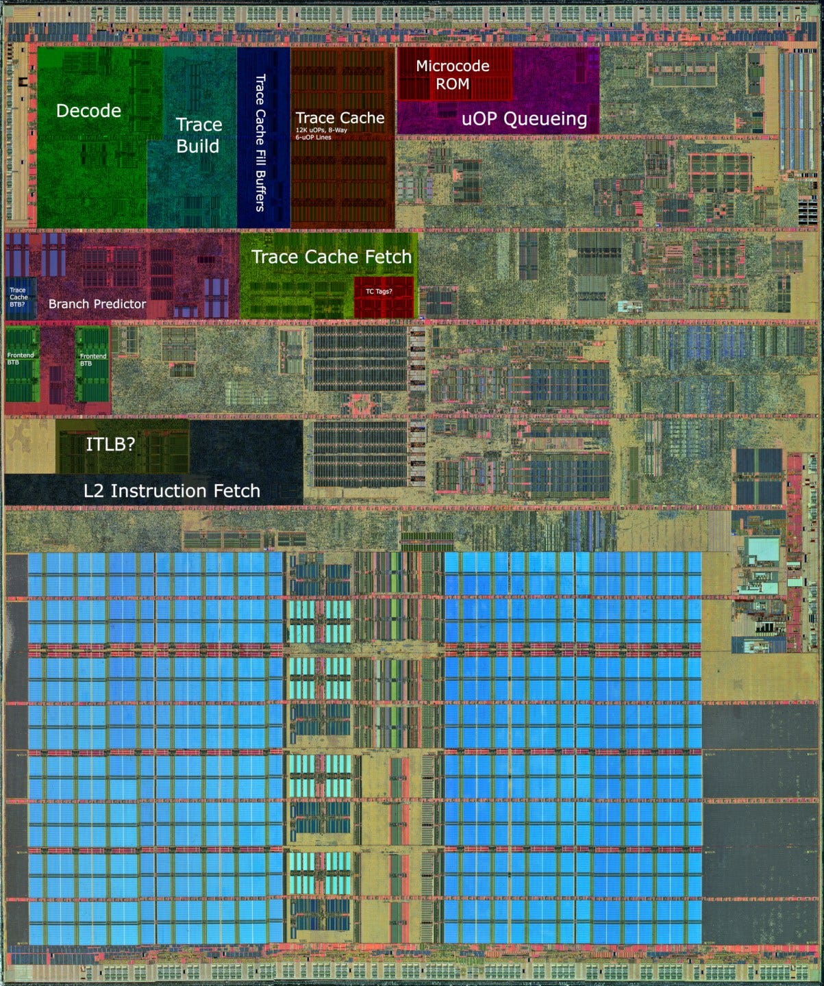
Storing decoded micro-ops means “instructions” fetched from the trace cache can be delivered with higher bandwidth, lower latency, and lower power. Testing instruction fetch bandwidth with 8-byte NOPs shows this advantage. If the average instruction length is too long, the L1i can’t feed the decoders fast enough. Hitting the trace cache bypasses this limitation.
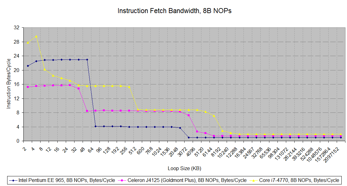
Micro-op caches found in AMD, ARM, and Intel’s modern CPUs use the same technique to allow higher instruction bandwidth at lower latency and lower power. But Netburst’s technique of caching traces was dropped, because it makes the cache very area inefficient. Micro-ops already tend to be larger than ISA instructions and that’s especially the case for x86 where variable length encodings mean higher space efficiency. Caching the same instruction more than once only exacerbates the capacity problem. According to Agner Fog, 90 nm Pentium 4 variants (and presumably later ones) have 64-bit micro-ops. The 12K entry trace cache would thus be implemented with 96 KB of raw storage, even though Intel’s whitepaper claims it “has a similar hit rate to a 8K to 16K byte conventional instruction cache”. That’s a serious problem in programs with large instruction footprints. And Intel’s immediate competitor, AMD’s Athlon, is bouncing around with a 64 KB instruction cache.
When large instruction footprints cause trace cache misses, Netburst is in serious trouble. It has to fetch instruction bytes from L2, and pass them through a 1-wide decoder. A conventional wide decoder can maintain a reasonable level of instruction throughput in the face of L1i misses, since lower level caches can still provide enough bandwidth to hand the decoders multiple instructions per cycle. But Netburst does away with that setup. Instruction throughput therefore drops like a rock once the trace cache is missed.

Along with being sent down the pipeline, micro-ops emitted by Netburst’s decoder are built into traces, which are filled into the trace cache. This trace building logic has to make a difficult tradeoff. It can more efficiently utilize trace cache capacity by breaking up traces to minimize duplicate instruction caching. Or, it can make longer traces to maximize trace cache fetch bandwidth. I’m guessing this logic block is complex and a nightmare to tune.
While flawed, Netburst’s instruction caching strategy had upsides. As mentioned before, skipping instruction decode has obvious latency, bandwidth, and power benefits. Starting with Sandy Bridge, Intel re-introduced micro-op caching to get those benefits for small code footprints. A much smaller micro-op cache is paired with a beefy conventional decoder and L1i cache. That setup gets the best of both worlds. Interestingly, Sandy Bridge’s micro-op cache remains 8-way set associative and uses 6 micro-op lines, just like Netburst’s trace cache. And unlike the micro-op cache found in AMD’s Zen CPUs, Intel’s modern micro-op caches are unable to cache micro-ops from the microcode sequencer. Instead, just like Netburst’s trace cache, a pointer to the microcode ROM is stored. These implementation detail similarities mean there’s a good chance Intel’s modern micro-op cache design retain a good chunk of Netburst trace cache DNA.
As a final note, imitation is most sincere form of flattery. AMD, ARM, and Samsung have all introduced some form of micro-op cache in their CPU architectures. Netburst’s trace cache led to Intel being a pioneer in this area.
Rename and Allocate
Once the CPU has an instruction’s corresponding micro-ops available, it’s time to allocate resources in the backend to track them.
Netburst has a 3-wide rename and allocate stage. While Netburst introduces a physical register based out-of-order engine, it doesn’t seem capable of move elimination. However, it is able to recognize zeroing idioms and break dependencies. Strangely, some zeroing idioms perform better than others

Nehalem (and Westmere)’s lower throughput for independent register to register MOVs could be caused by a retired register file (RRF) bandwidth limitation. Intel’s P6 architecture handled register renaming by using result fields in the reorder buffer (ROB) as renamed registers, for instructions pending retirement. At retirement, instruction results are copied from the ROB to the RRF.
A peculiar feature of the P6’s out of order engine is that the scheduler holds input values for instructions waiting to be executed. The renamer therefore has to write input values into the scheduler if they won’t be forwarded from another in-flight instruction. If these input values come from an instruction that has already retired, the renamer has to read from the RRF. According to Agner Fog, the RRF in Nehalem (and Westmere) only has three read ports. Netburst eliminates this bottleneck by using separate register files that hold both speculative and architectural results.
Out of Order Execution Engine
With the Pentium 4, Intel completely re-architected the out of order engine. As mentioned above, it no longer uses a ROB+RRF scheme. Instead, the ROB holds pointers to register file entries. The same applies to the renamer, where the register alias table for architectural, known-good state also holds pointers to register files. This setup, which we’ll refer to as a PRF based scheme, allows less data movement. Pointers to register file entries can only be a few bits in size. For example, you’d only need seven bits to index into a 128 entry register file, while an integer register is 64 bits wide. This is especially important for SIMD registers, which can be much larger. Trying to move several 128-bit values at retirement would probably consume quite a bit of power.
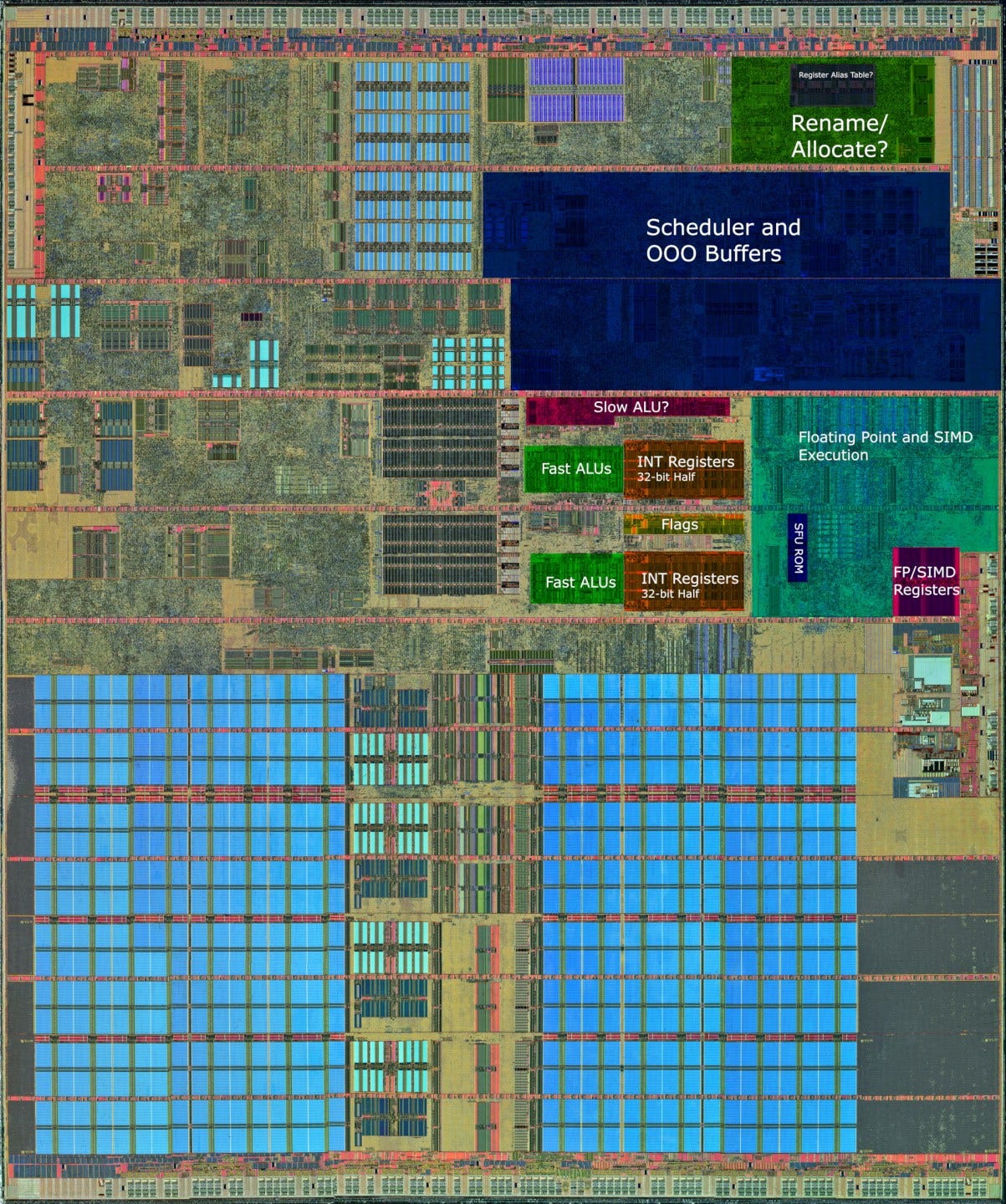
A PRF based scheme also lets engineers set register file and ROB sizes independently. Not every instruction will write a result to a register, with common examples being branches and stores. Using separate register files thus makes ROB size increases cheaper. Finally, the PRF-based scheme allows renamer tricks like move elimination, where instructions that copy values between registers can be “executed” within the renamer by manipulating the speculative register alias table’s pointers.
In general, Netburst’s out of order structures are massive and not matched in size until Nehalem debuted in 2008. But there’s a sinister reason behind this. Agner Fog found that Netburst can’t cancel erroneously fetched instructions until retirement, for example from a branch mispredict. Omitting the ability to squash bogus instructions probably let Intel simplify the pipeline, and achieve higher clocks in the process. But it means the out of order engine has to keep tracking bogus operations until they’re completed, reducing effective reordering capacity. Netburst’s structure sizes were likely increased to compensate.
This is especially obvious with scheduling capacity. Even compared to more modern designs, Netburst can track a monstrous number of instructions waiting for an execution unit.

Netburst also differs from other Intel high performance designs in using a distributed scheduler for math operations. This distributed scheduler lets Intel keep port count low for each scheduling queue, reducing area and power requirements. Another unique feature is that multiple scheduling queues share a single dispatch port, and arbitrate for access.

In terms of execution units, Netburst has a rather convoluted setup. There are four dispatch ports, but two of these are connected to hot-clocked integer ALUs that can execute two operations per core cycle. A 3-wide core that can do four ALU operations per cycle is strange, as the ALUs are guaranteed to be under-fed. But Netburst is not normal. Remember how it can’t cancel bogus micro-ops before retirement? That wastes execution resources too. The wastefulness doesn’t stop there because L1D misses are handled rather inefficiently. Netburst’s schedulers will send loads for execution assuming they hit L1D. If they miss L1D, they’re sent back into the schedulers to be repeatedly executed until the correct data arrives. This “instruction replay” extends to dependent instructions too.
This very high throughput ALU setup is thus dictated by Netburst’s inefficiencies. Having what’s basically four ALUs on a 3-wide core will not give you superior integer performance, but that’s not what they’re there for. They’re there to crunch through all the bogus work, while having enough throughput left over to handle real work.
Store Forwarding, and Load/Store Unit Details
A CPU’s load/store unit has to ensure that memory operations appear to be executed in-order. If a store instruction writes to a location, a future read to that location should give back what the store wrote. This may seem intuitively simple, but an out-of-order CPU can have a lot of memory operations in flight. A store instruction can’t write its data out to the memory hierarchy until it retires. Every load therefore has to determine whether it should get its data from a prior store, or from the memory hierarchy. The load/store unit has to compare in-flight load and store addresses to ensure this happens correctly.

Netburst’s memory dependency checking mechanism is pretty primitive. Store forwarding is only successful for exact address matches and no cacheline boundaries are crossed. This ‘happy path’ case is handled with 5-6 cycle latency, which is pretty typical. However, every other store forwarding case fails. These failure cases are astoundingly bad. If the load is contained within the store but addresses don’t match exactly, Netburst takes over 50 cycles to resolve the situation. That’s over twice the cycles typically seen with other CPUs, and it’s not even the worst.
If forwarding fails and the load is misaligned (crosses a cache line), latency increases to 89 cycles. If the store is misaligned it’s 125 cycles. If both are misaligned, Netburst suffers an absolutely disgusting 165 cycle penalty. These can be considered edge cases, but most other CPUs can handle them in a couple dozen cycles at most. The Intel Technology Journal’s paper on the Netburst architecture’s introduction noted that a “disallowed store-to-load forwarding case can be quite costly, in terms of performance loss.” They weren’t kidding.
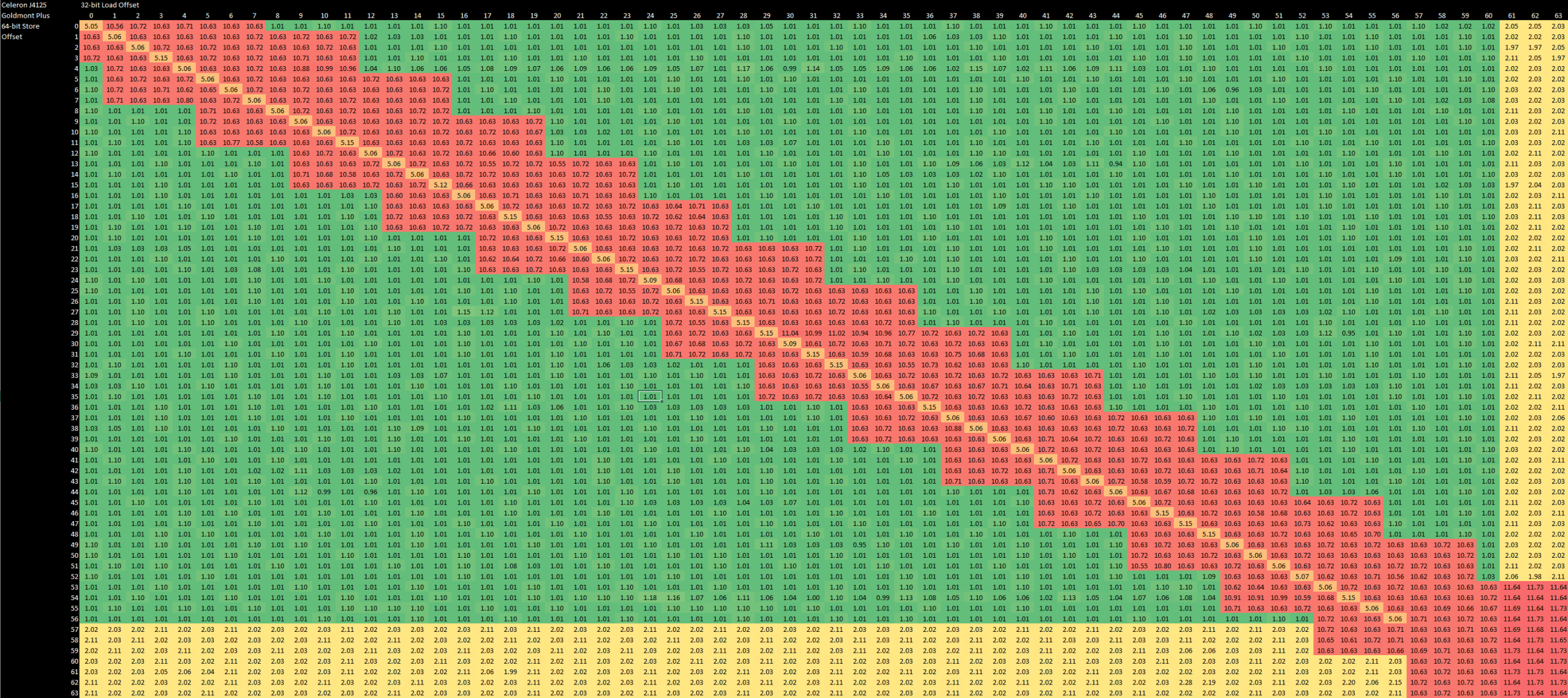
Misaligned data accesses are unreasonably expensive on Netburst, even if there are no nearby instructions that could cause memory ordering issues. If an access crosses a cacheline boundary, it’s one thing it to take two cycles because it gets executed as two operations within the load/store unit. That’s a light penalty that will easily be hidden by out of order execution. It’s another to faceplant and take 23 cycles, which Netburst does for a misaligned load. And it’s yet another step in the wrong direction to die in a hole for around 105 cycles when a store crosses a cacheline boundary. But Netburst does exactly that.
Caching and Memory Access
Like its instruction side, Netburst’s L1 data caching setup is fine for programs with small data footprints, but suffers from low capacity for larger working sets. The 16 KB data cache that comes with later revisions of Netburst is definitely better than the laughably small 8 KB cache featured in Willamette (180 nm) and Northwood (130 nm) cores. But this L1D size increase also increased latency from two cycles to four. For perspective, AMD’s Athlon has a 64 KB L1D with three cycle latency.
That means Netburst’s L1D has worse latency than AMD’s. This applies to actual time latency as well, since the Pentium Extreme Edition 965 doesn’t have enough of a clock speed advantage over AMD’s Athlon X2 6000 to close the gap. Building such a large L1D cache and maintaining 3 cycle latency even for indexed addressing modes is quite an achievement, and AMD should be proud of that.
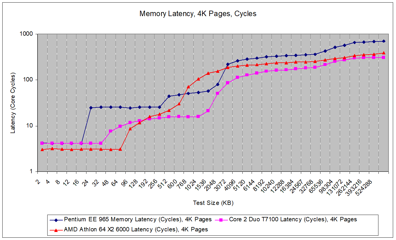
The Pentium EE 965 has a 2 MB L2 for each core, with a latency of about 25 cycles. AMD’s L2 is smaller and takes fewer cycles to return data, but Netburst’s higher clocks close the latency gap. That gives Intel a larger L2 with similar latency. Intel’s later Core 2 architecture has L2 characteristics similar to AMD’s, but shares a single L2 cache between both cores.

Consumer CPUs in the mid 2000s typically used simple, two-level caching setups. Netburst is no different. A L2 miss goes right out to memory. Intel’s designs of the area access memory by going through a front side bus to the chipset’s northbridge, where the memory controllers are located. This extra off-chip hop increases latency, and means that both the Pentium EE 965 and Core 2 suffer higher memory latency than AMD’s Athlon.
This latency can be exacerbated by TLB misses. If we use 2 MB pages, allowing each TLB entry to cover 2 MB instead of 4 KB, we can see how Netburst suffers from address translation penalties. At the 512 KB test size, we see a 18.35 clock cycle latency delta (4.92 ns) between 4 KB and 2 MB pages. This only grows as test size increases and page walks start missing cache.
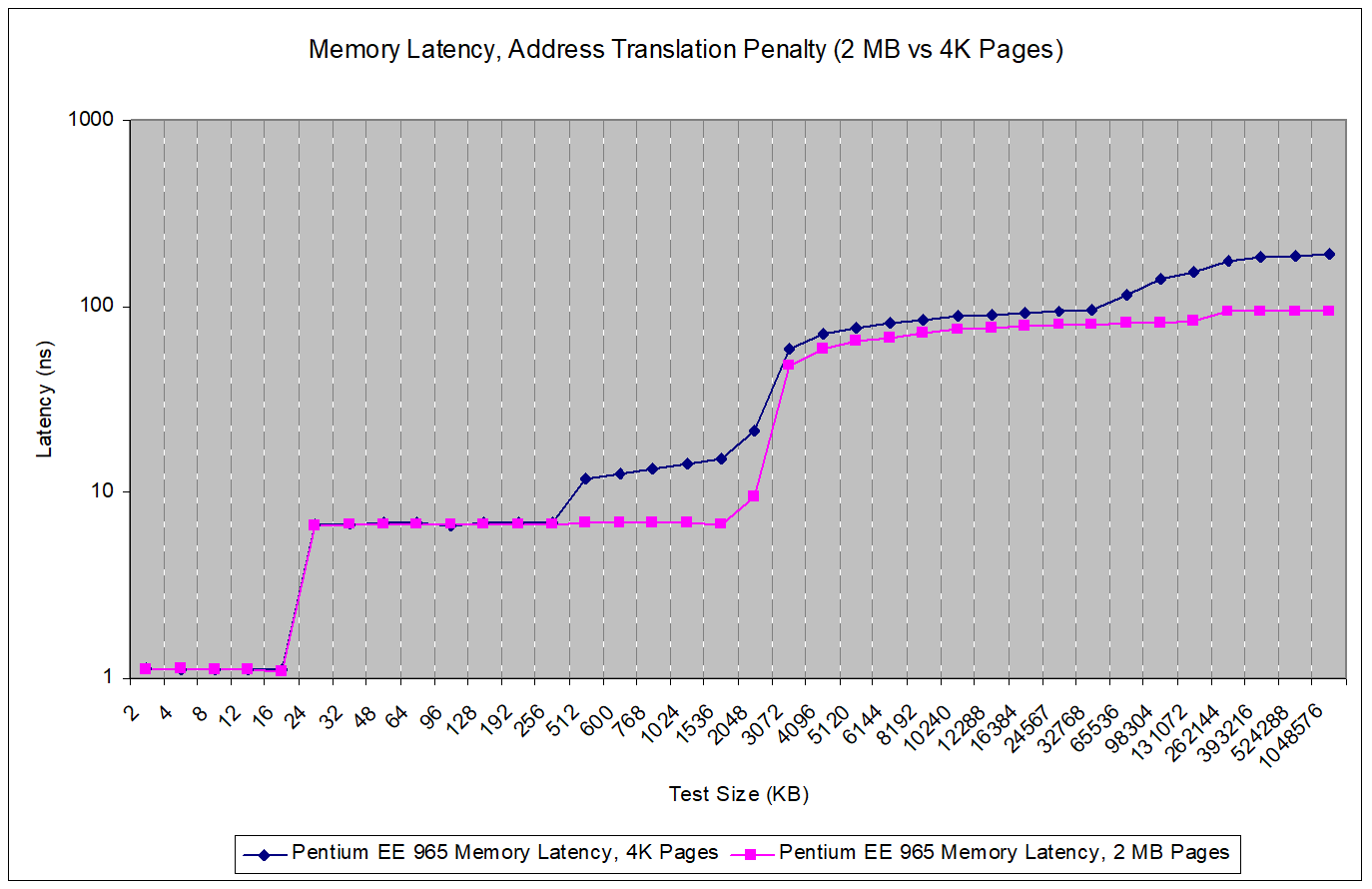
In an absolute time sense though, raw memory latency isn’t so bad. With 2 MB pages used to minimize address translation overhead, memory latency is somewhere around 90 ns. That’s roughly comparable to Tiger Lake (i7-11800H)’s memory latency, even though Tiger Lake benefits from an integrated memory controller.
Bandwidth
Netburst makes significant gains in bandwidth compared to previous generations of Intel CPUs. Versus the P6 based Pentium M, L1D load width has doubled. Alongside that, Netburst’s L2 cache bandwidth is dramatically better. Old P6 chips had the L2 attached off a backside bus, with some variants using external L2 SRAM chips. Netburst moves to a far more integrated L2 setup.

Against Westmere, Netburst falls behind everywhere. Intel made huge advances in their caching strategy in the years after Netburst’s retirement. Westmere’s L3 is particularly impressive. Despite being several times larger than Netburst’s L2, it can provide roughly comparable bandwidth to a single thread.
The only bright spot for the Netburst is its 16 byte per cycle load capability combined with very high clock speeds. That lets the Pentium EE 965 deliver higher L1D bandwidth than Westmere. But that’s about it. Even against a Westmere server chip, Netburst’s clocks aren’t quite high enough to pull an advantage anywhere else.

In terms of multithreaded bandwidth, we unfortunately don’t have data from contemporary chips to make anywhere close to a sensible comparison. So here’s a comparison between the dual core, quad thread Pentium Extreme Edition 965, and the quad core Pentium J4125. This Goldmont Plus chip has the same amount of total L2, but shares it across four cores instead of having a private L2 cache per core. And even with that setup, it achieves higher L2 bandwidth than Netburst does.

In DRAM sized regions, the Pentium EE 965 achieves about 6.8 GB/s of bandwidth. Using four threads actually lowers memory bandwidth. It drops to 5.86 GB/s, suggesting that contention between threads is not handled very well. The chip tested here was given dual channel DDR2-533, so we’re seeing about 80% bandwidth efficiency when a single thread is used, and 68.7% with all threads. With a single channel DDR4-2133 setup, the Celeron J4125 achieves 76.9% bandwidth efficiency when four cores are loaded, but just 38.8% with a single core. In that respect, it’s nice that Netburst can utilize all available bandwidth with a single thread, but that’s also because there’s not much memory bandwidth available to start with.
Write Bandwidth
For a few articles, we didn’t cover write bandwidth in depth to keep things short. But Netburst forces this, because it uses a write-through L1 data cache.
Most CPUs we use implement write-back L1D caches. When you write to such a cache, the modified data is held there and not written further down the memory hierarchy until it’s kicked out of the cache, either to make room for new data or to maintain cache coherency. With a write-through cache, a write is immediately written through to the next level down the memory hierarchy. As far as write bandwidth goes, a write-through cache may as well not exist.

On Netburst, that means write bandwidth is less than a quarter of read bandwidth. Within L2 sized regions, we get under four bytes per cycle, or around 13.27 GB/s. That’s extremely poor because every write instruction will be subject to that bandwidth limitation. While most programs execute more memory reads than writes, the read-to-write bandwidth ratio here is more than a bit off. For example, when encoding video with libx264 (on Sandy Bridge), 28.6% of instructions were loads, while 11.86% were stores, for a 2.41:1 load to store ratio. The ratio of load to store bandwidth on Netburst is a staggering 4.46:1. The situation is made worse by the small L1D and capacity-inefficient trace cache. Both of those mean increased read traffic to L2, which will compete with write traffic.

Of course, there are justifications behind using a write-through cache. Much like skydiving without a parachute, a write-through cache removes extra steps, making the process simpler and easier. For example, you have to carefully fold a parachute, and bring a backup chute. Similarly, a write-back cache needs robust error correction because data corruption can screw up the only modified copy of something. A write-through cache never holds the only copy of modified data. If an error is detected, it can simply reload the affected data from the next level down. You also have to remember to open a parachute in conventional skydiving. Similarly, a write-back cache has to remember what data was modified, so that it knows whether to write-back cache lines when they’re evicted.
However, the results in both cases can be sub-optimal. Just as falling through the ground at terminal velocity can negatively impact your health, writing data through a cache can negatively impact performance. Netburst’s small, write-through L1D was not used again on Intel’s later architectures.
Putting it Together
Netburst was not successful. It’s an architecture characterized by excellent fast-path performance and horrifying penalties once code does something it doesn’t expect. Its pipeline was prone to doing excessive amounts of unnecessary work, thanks to handling cache misses via replay and its inability to cancel bogus operations. The result is an architecture that in many ways looks very impressive on paper, but ends up suffering a combination of very poor power efficiency and poor performance per clock.
Then, clock gains from new process nodes didn’t pan out as expected, and the architecture never reached the astronomically high clock speeds it was meant to hit. The architecture’s performance per clock was so bad that the higher clock speeds it actually achieved weren’t enough to cope, especially as AMD also gained clock speed from process node improvements.
In my opinion, this is the result of Intel biting off more than they could chew. Netburst debuted a mountain of new microarchitecture techniques. Some of these had been implemented by other companies, but were new to Intel. In general, the more you depart off the known path, the more risk you take. More changes mean more moving parts to tune and validate. Intel clearly took on way too much risk. Just to put down what Intel tried to bring into play:
With so many moving parts, I strongly suspect Intel didn’t have a good picture of how penalties caused by tradeoffs in different parts of the pipeline could exacerbate each other.
Some of these items are a lot more significant than what a row on a table would suggest. For example, moving from a P6 style ROB+RRF scheme to a PRF based one means you don’t get a register for free just by allocating a ROB entry. You need to keep separate freelists for your register files. I imagine that complicates exception handling – you can’t cancel a batch of bogus ops after a branch mispredict by implementing the ROB as a circular buffer and setting the “head” back to the mispredicted branch. Instead, every register allocated to a bogus operation has to be added back to the respective register file’s freelist. That may have driven the decision to not bother cancelling bogus operations after a branch mispredict, and just have the retirement unit deallocate registers allocated to bogus operations. That in turn forces larger out of order structures to handle the overhead created by tracking those bogus operations for longer than is strictly necessary.
But it’s wrong to write off Netburst as just a failure. Some of the fundamental ideas behind the architecture were definitely flawed. Emphasizing clock speed at the cost of extreme penalties for “corner cases” that aren’t actually uncommon turned out to be a pretty bad strategy. But Netburst served as a learning platform for Intel. The company implemented a variety of new microarchitecture techniques for the first time, and saw how they performed in practice. They figured out what worked and what didn’t. They took years to gather data and tune novel features like HyperThreading.
Going through Netburst’s architecture again, we can see how the good parts came back to enable Sandy Bridge’s success.

Building off this Netburst experience meant Intel wasn’t internally reinventing the wheel when corresponding features were put into Sandy Bridge. Instead, Sandy Bridge hit the ground running. And that architecture was a massive hit, destroying AMD’s presence across every CPU market sector for years to come. Then, they hammered home that advantage by making conservative but steady progress, alternating between microarchitecture evolution and process node ports to keep risk low. And the foundation for this success was built by the infamous Netburst architecture.
If you like our articles and journalism and you want to support us in our endeavors then consider heading over to our Patreon or our PayPal if you want to toss a few bucks our way or if you would like to talk with the Chips and Cheese staff and the people behind the scenes then consider joining our Discord.
Credits and Setup Info
Big thanks to cha0s for setting up the system and running tests. The Pentium Extreme Edition 965 was running on an Asus P5W64 WS Pro board (Intel i975X chipset) with a 1066 MT/s FSB. Dual channel DDR2-533 3-3-3-9 was used.
The Athlon 64 X2 6000+ (Brisbane, 65nm) latency test was run by catsay. That system had a dual channel DDR2-800 5-5-5-18 setup and an Asus M2N4-SLI board (Nvidia nForce4 SLI chipset).
Extras
Northwood uses an earlier version of the Netburst architecture, implemented on the 130 nm process. It’s notable for featuring a very small, but very fast 8 KB L1D with just two cycle latency. The L2 on Cedar Mill and Northwood have similar latency in cycle counts, but Cedar Mill’s L2 is larger.

Cedar Mill also achieves higher clocks, which makes its L2 both larger and faster. The same doesn’t apply to the L1 cache, where Northwood delivers lower latency.

Intel probably went from a 8 KB, 2 cycle L1D to a 16 KB, 4 cycle one because 8 KB is ridiculously small. Prescott and Cedar Mill feature 64-bit support, and 64-bit code tends to have larger memory footprints. That makes a 8 KB L1D even more nonsensical. Relaxing L1D timings may also have helped Prescott scale to higher clocks.
Results from the graphs above are from Ashley89. That system was equipped with DDR-400 3-4-4-8 and an Intel i865P chipset.