
Intel Renames Oregon Fab: Gordon Moore Park. Adds +270k sq ft, 18A Node now 2024

If there’s one thing that’s cheaper than building a new fab, it’s expanding an existing one. Intel’s Oregon D1 facility has been the hub of all of its technology advancements over the past 20 years, whereby Intel will trial new manufacturing processes before transferring them to other fabs around the world. As you can imagine, the site in Hillsboro is a big facility, sprawling over some 530 acres and hiring 14000 employees, making Intel the biggest employer in Portland. As was previously announced, Intel would be expanding its fab at Hillsboro to accommodate more tools, more capacity, and more research. Today, that expansion is officially being opened: enter D1X Mod 3.
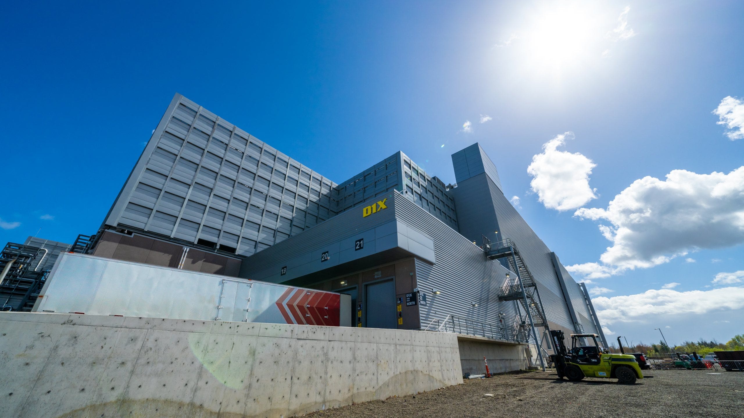
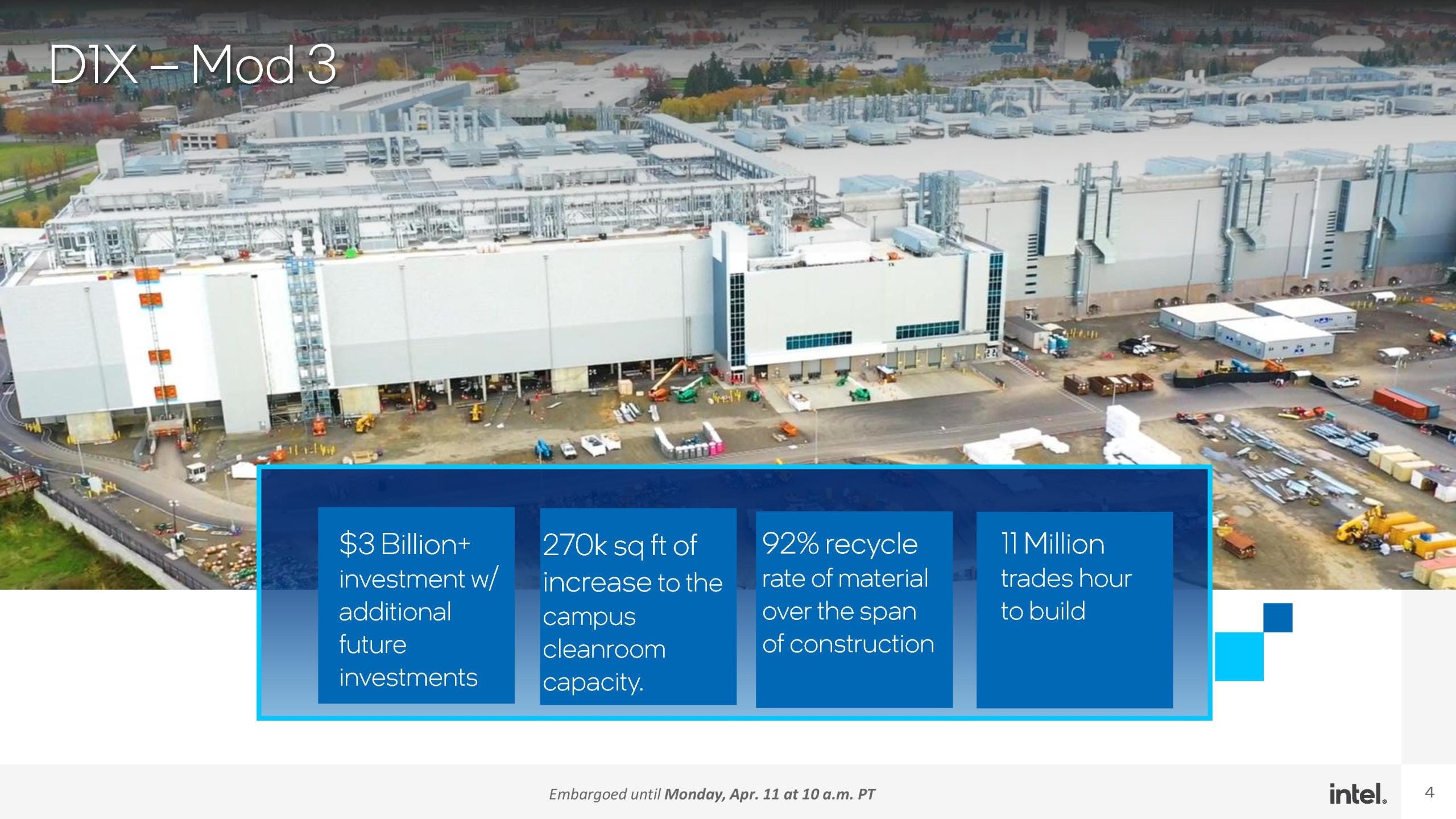
The new Mod 3 extension of the D1X fab is an impressive, with Intel stating that it has created 270,000 square foot more clean room space, or the equivalent of 3.5 football fields (for context, the new site announced at Magdeburg is only 2 football fields, or 165k square feet). I visited the facility back in December, where it seemed the construction of the shell was complete, the clean room area was already integrated into the rest of D1X, but they were in the process of installing tools. Intel stated to us that technically D1X Mod 3 could have been opened at a variety of times, although they chose this date because (a) we’re moving to warmer weather for the event, and (b) it’s a time they could get the local government dignitaries to attend, such as a state governor.
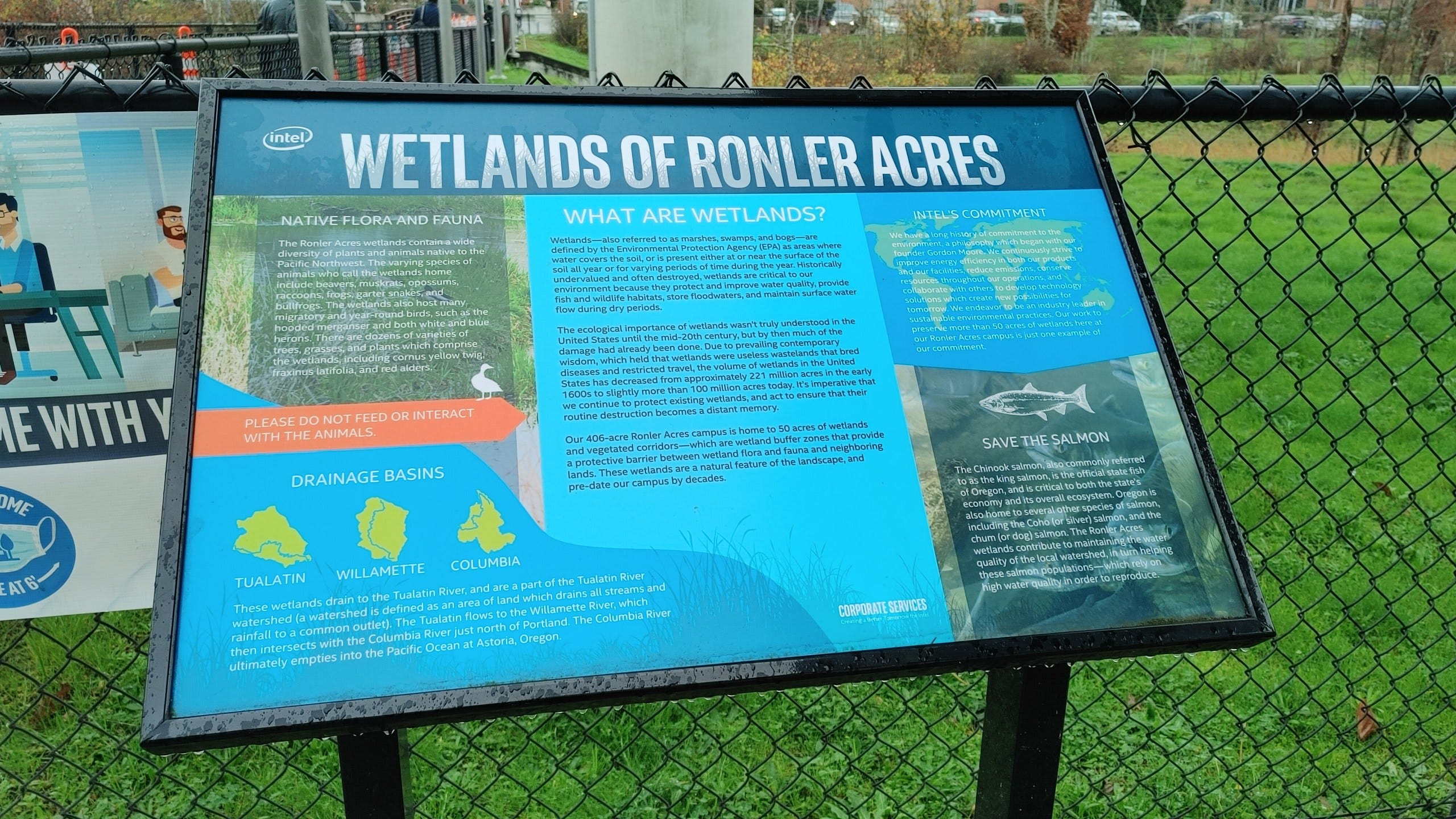
Intel’s full facility, including the fabs and the research areas, is on a site called Ronler Acres. As part of the announcement today, Ronler Acres is to be renamed after one of the companies co-founders, and the new name is the ‘Gordon Moore Park’. The full cost of the expansion and renaming is north of $3B+, although this doesn’t include all the extra equipment for the cleanroom. Currently the facility isn’t full of hardware – part of that extra 270k square foot is for future expansion as more tools are needed and more are delivered. With current lead times for semiconductor tooling supposedly going beyond 18 months, this is perhaps to be expected. Intel states that the Gordon Moore Park site will host the first High-NA machines from ASML, and be the site of ramping the technology for customer high-volume manufacturing in 2025.

On that point, part of today’s announcement is a continuation of what we heard from Dr. Ann Kelleher, Intel’s VP of Technology Development – Intel is enabling a dual track effort for future process node technologies such that regular EUV can be used all the way down from Intel 4 to Intel 3 to Intel 20A to Intel 18A (and beyond), while High-NA EUV will intercept that roadmap when it is ready, and technologies will be able to be built with either in the event that High-NA takes longer to implement.

Intel also shed some light on an internal test node that they are working on. The mantra from the CEO Pat Gelsinger has been to deliver 5 process node technologies in 4 years, however internally there is another node that’s being given equal treatment. Intel has already announced PowerVia, its technology for backside power delivery due to intercept the timeline with Intel 20A along with RibbonFET, but in order to get a handle on the new manufacturing techniques required, Intel has a ‘Risk Reduction Test Node’ to get to grips with it before mainstream production.
This test node uses the same Intel 4/Intel 3 FinFET designs for its transistors, but separates the power lines and signal layers on to separate sides of the transistor. In Intel 20A, the transistors in the middle of this sandwich will be RibbonFETs, but the test node for PowerVias is needed to make sure that yields can scale. Intel stated that this test node, a sort of ‘Intel 3b’, will still get the same attention for risk management and yield scaling as any other regular production node. We should state that Intel has mentioned this risk node before, but we were under the impression it was being done on a 14nm or 10nm process which was already high-yielding, rather than the leading edge that still has to reach that level.
Intel was asked if this Intel 3b test node, using FinFET + PowerVia, would ever reach productization – the answer was that although it’s getting the same treatment as a production node, there are currently no plans to move it to full production, and there are no customer chips being designed with it. This last element is important, as we know that customers are already working with Intel 3 and Intel 20A product design flows ready for when Intel can make those manufacturing processes available.
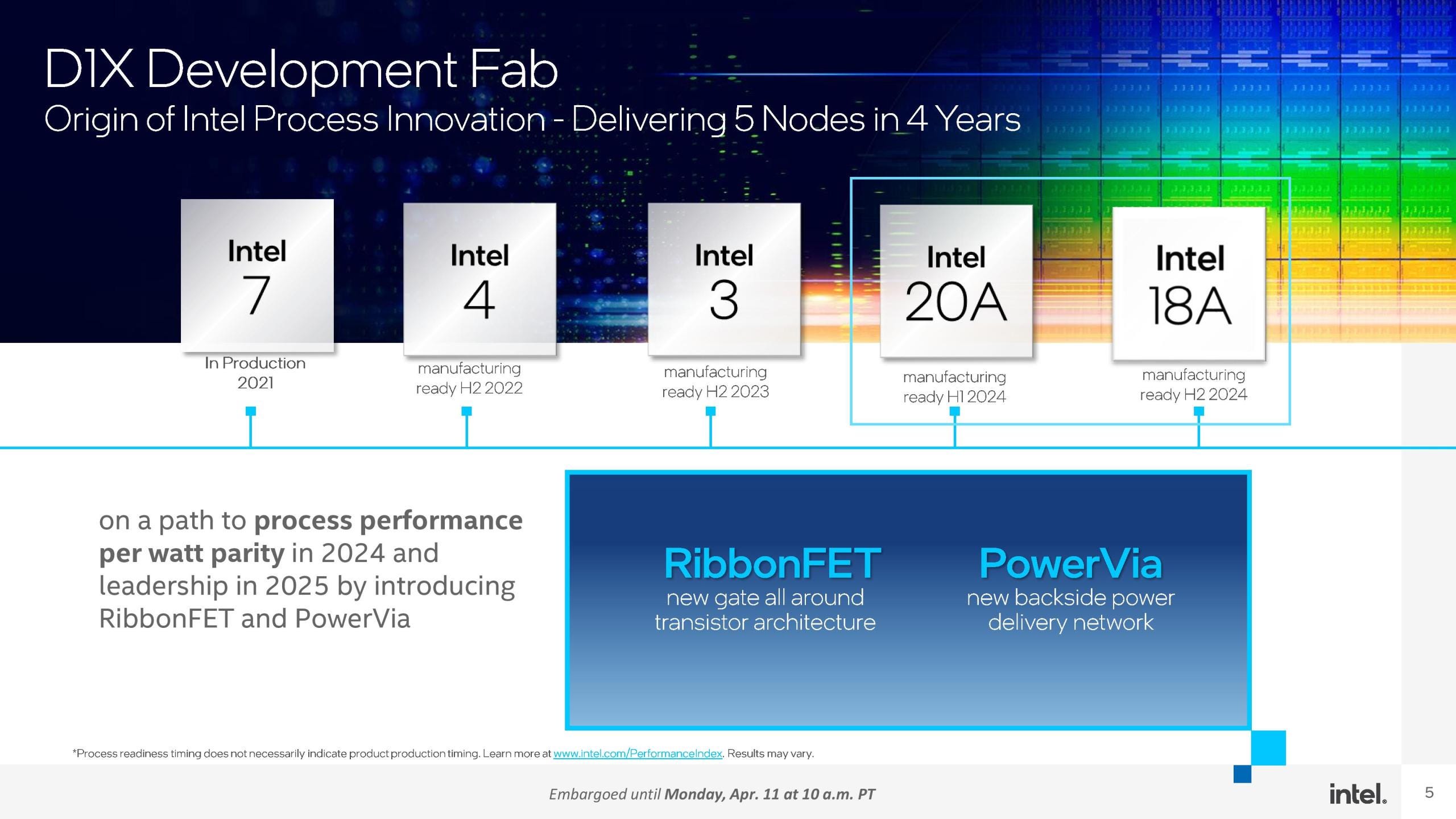
The last final note of the announcement is some timeline adjustment with Intel’s future node technologies. To date, Intel has stated that the Intel 18A node is due for 2025, but this date is now changing to ‘late 2024’, pulling in the date by at least a quarter. Intel confirmed that is because some of the key metrics they use to determine when the technology will be ready are already meeting targets ahead of schedule, and so enough confidence was there to make this change. It means that in 2024, we should expect 20A in the first half, and 18A in the second half. That being said, some in the semiconductor space are wondering if 20A is somewhat of a pipecleaner, and 18A is meant to be the long-life node, akin to where 14nm is today on Intel’s roadmap.
Written by Dr. Ian Cutress, Chief Analyst of More Than Moore
If you like our articles and journalism and you want to support us in our endeavors then consider heading over to our Patreon or our PayPal if you want to toss a few bucks our way or if you would like to talk with the Chips and Cheese staff and the people behind the scenes then consider joining our Discord.
 | A guest post by
|